-
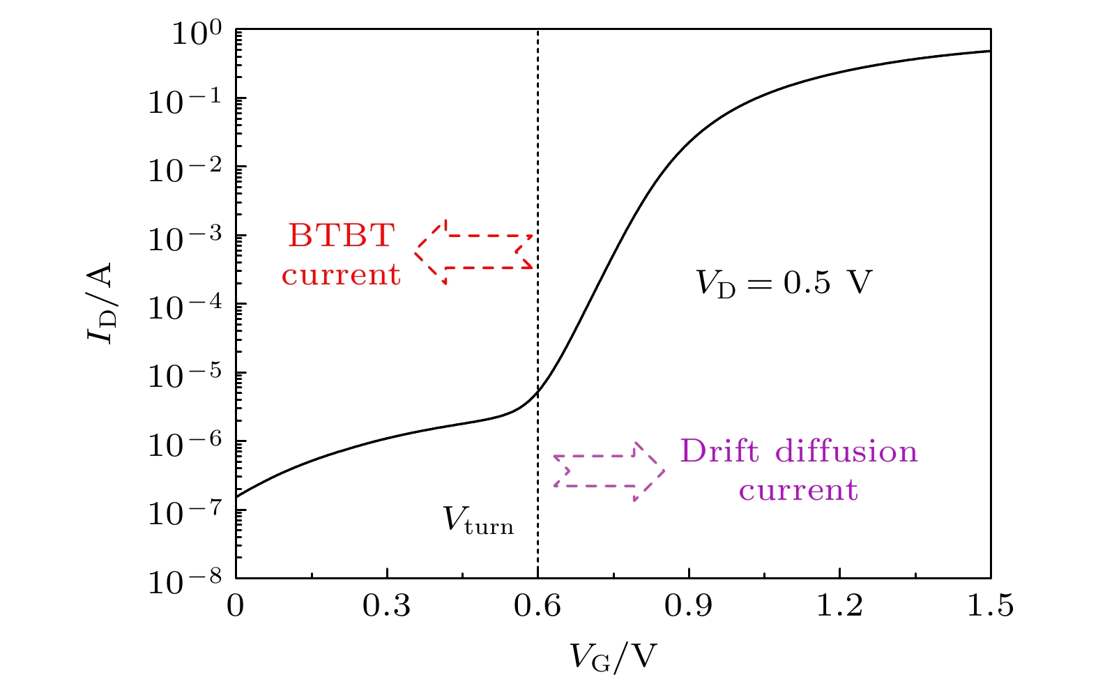
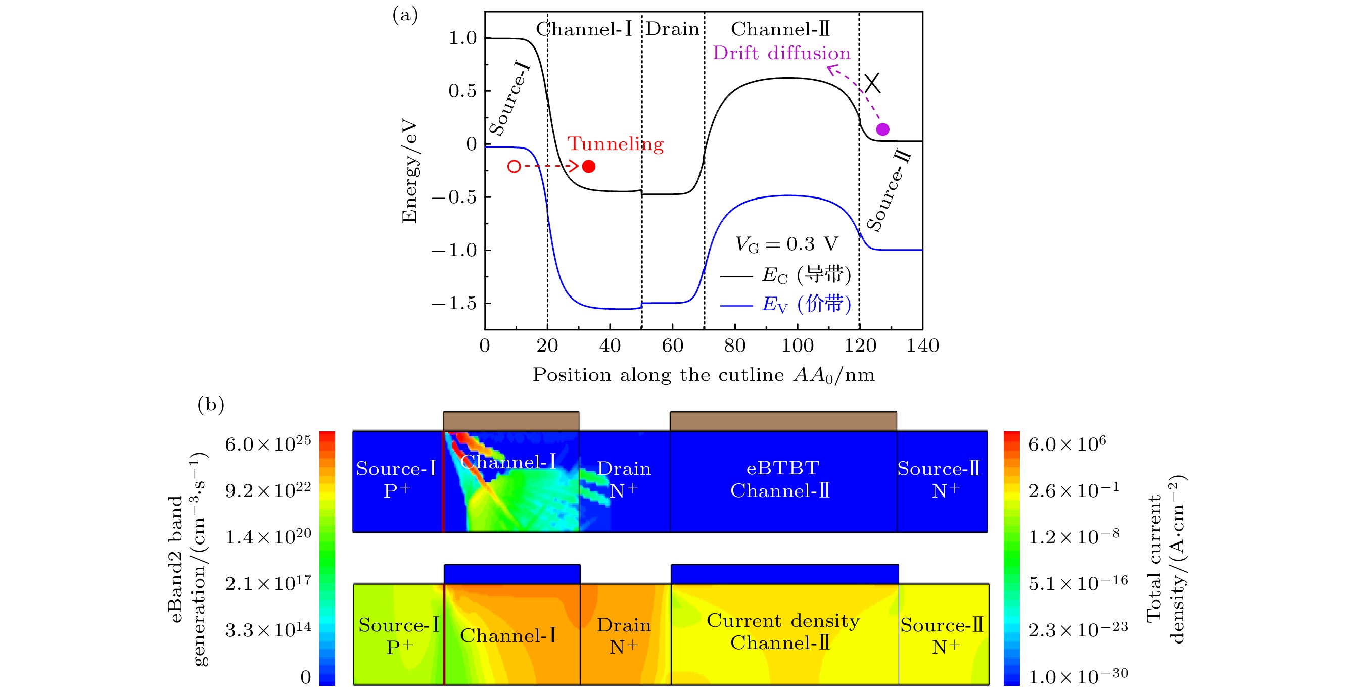
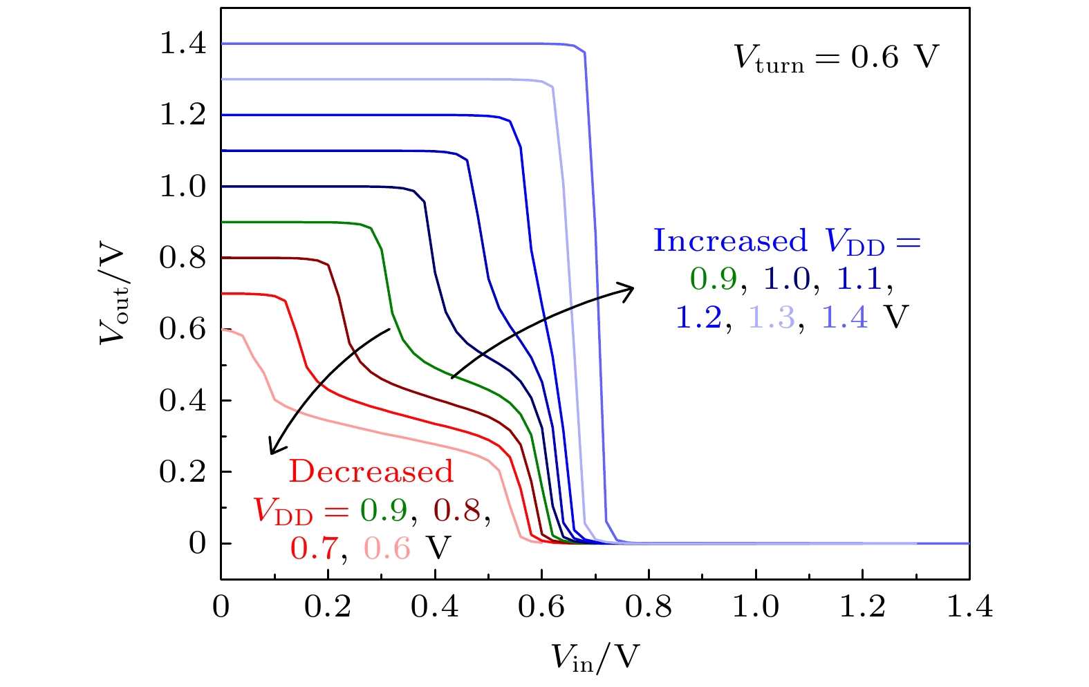
With the development of complementary metal-oxide semiconductor (CMOS) technology, the feature size of mental-oxide-semiconductor field-effect-transistor (MOSFET) is continuously shrunk, the short channel effect becomes more and more serious, which makes the static power consumption increase, and now the static power consumption becomes a main source of the power consumption of the integrated circuits. Currently, the performance of CMOS binary logic processor is approaching a bottleneck; therefore the ternary logic becomes a research hotspot to promote the development of high-performance low-power integrated circuits. Compared with binary logic, ternary logic possesses a strong data expression capability, which can not only improve the data density, but also reduce the circuit power consumption and the system complexity. However, using binary devices to build ternary logic circuits requires a large number of components, and even the passive components, which makes it impossible to leverage the advantages of ternary logic. The other method of implementing ternary logic is to utilize innovative two-dimensional materials. This method requires a small number of components and obviates the need for passive components, but it faces the problem that the fabrication process is not mature and cannot be mass-produced. To solve these problems, in this paper by combining the tunneling and the drift diffusion mechanism, we propose a tunneling metal-oxide-semiconductor field-effect transistor (TMOSFET) with three-state characteristics that make it highly suitable for ternary logic design. Compared with other ternary logic schemes, the ternary inverter based on TMOSFET has the same circuit structure as binary inverter, which can simplify the circuit design. In this paper, the operational mechanism of this ternary inverter is studied, and the condition of three-state output of inverter is analyzed. It is found that when the operating voltage VDD and the device turning voltage Vturn satisfy VDD/Vturn ≈ 1.4, the input voltage ranges of the three output states are equivalent. In addition, the influence of TMOSFET transfer characteristic on this ternary inverter is also analyzed. This has certain reference significance for designing and studying ternary logic circuits in future.
-
Keywords:
- tunneling field effect transistor /
- mental-oxide-semiconductor field-effect-transistor /
- ternary inverter
[1] 芦宾, 王大为, 陈宇雷, 崔艳, 苗渊浩, 董林鹏 2021 70 218501
 Google Scholar
Lu B, Wang D W, Chen Y L, Cui Y, Miao Y H, Dong L P 2021 Acta Phys. Sin. 70 218501
 Google Scholar
[2] Roy K, Mukhopadhyay S, Mahmoodi-Meimand H 2003 Proc. IEEE 91 305
 Google Scholar
[3] Frank D J 2002 IBM J. Res. Dev. 46 235
 Google Scholar
[4] Srivastava A, Venkatapathy K 1996 VLSI Design 4 75
 Google Scholar
[5] Hurst 1984 IEEE Trans. Comput. C-33 1160
 Google Scholar
[6] Jo S B, Kang J, Cho J H 2021 Adv. Sci. 8 2004216
 Google Scholar
[7] Zhu Y, Lu H, Zhang Y, Sun J, Lyu Z, Lu B 2022 IEEE 16th International Conference on Solid-State & Integrated Circuit Technology Nangjing, China, October 25–28, 2022 p1
[8] Tavanaei A, Ghodrati M, Kheradpisheh S R, Masquelier T, Maida A 2019 Neural Networks 111 47
 Google Scholar
[9] Ghosh-Dastidar S, Adeli H 2009 Int. J. Neural Syst. 19 295
 Google Scholar
[10] Esser S K, Merolla P A, Arthur J V, Cassidy A S, Appuswamy R, Andreopoulos A, Berg D J, McKinstry J L, Melano T, Barch D R, di Nolfo C, Datta P, Amir A, Taba B, Flickner M D, Modha D S 2016 PNAS 113 11441
 Google Scholar
[11] Kim H W, Kim S, Lee K, Lee J, Park B-G, Kwon D 2020 IEEE Trans. Electron Devices 67 4541
 Google Scholar
[12] Mouftah H T, Smith K C 1982 IEE Proc. 129 270
 Google Scholar
[13] Heung A, Mouftah H T 1985 IEEE J. Solid-State Circuits 20 609
 Google Scholar
[14] Gan K J, Lu J J, Yeh W K, Chen Y H, Chen Y W 2016 Eng. Sci. Technol. Int. J. 19 888
 Google Scholar
[15] Gan K J, Tsai C S, Chen Y W, Yeh W K 2010 Solid-State Electron. 54 1637
 Google Scholar
[16] Nourbakhsh A, Zubair A, Dresselhaus M S, Palacios T 2016 Nano Lett. 16 1359
 Google Scholar
[17] Shim J, Jo S H, Kim M, Song Y J, Kim J, Park J H 2017 ACS Nano 11 6319
 Google Scholar
[18] Huang M, Wang X, Zhao G, Coquet P, Tay B 2019 Appl. Sci. 9 4212
 Google Scholar
[19] Fei W, Trommer J, Lemme M C, Mikolajick T, Heinzig A 2022 InfoMat 4 e12355
 Google Scholar
[20] Vanlalawpuia K, Bhowmick B 2019 IEEE Trans. Electron Devices 66 4439
 Google Scholar
[21] Talukdar J, Rawat G, Mummaneni K 2020 Silicon 12 2273
 Google Scholar
-
表 1 n型TMOSFET结构参数
Table 1. Structure parameters of n-type TMOSFET.
Parameter Symbol Value Source length LS/nm 20 Source thickness TCh/nm 10 Source Ⅰ doping (P+) NSⅠ/(1019 cm–3) 1 Source Ⅱ doping (N+) NSⅡ/(1019 cm–3) 1 Channel Ⅰ length LCⅠ/nm 30 Channel Ⅱ length LCⅡ/nm 50 Channel I doping (N+) NCI/(1016 cm–3) 1 Channel Ⅱ doping (N+) NCⅡ/(1016 cm–3) 1 Drain length LD/nm 20 Drain doping (N+) ND/(1019 cm–3) 1 Gate oxide thickness TOX/nm 2 Gate WorkFunction Ⅰ WFⅠ/eV 3.37 Gate WorkFunction Ⅱ WFⅡ/eV 5.02 表 2 p型TMOSFET器件参数
Table 2. Structure parameters of p-type TMOSFET.
Parameter Symbol Value Source length LS/nm 20 Source thickness TCh/nm 10 Source Ⅰ doping (N+) NSⅠ/(1019 cm–3) 9 Source Ⅱ doping (P+) NSⅡ/(1019 cm–3) 1 Channel Ⅰ length LCⅠ/nm 30 Channel Ⅱ length LCⅡ/nm 50 Channel Ⅰ doping (P+) NCⅠ/(1016 cm–3) 1 Channel Ⅱ doping (P+) NCⅡ/(1016 cm–3) 1 Drain length LD/nm 20 Drain doping (P+) ND/(1019 cm–3) 1 Gate oxide thickness TOX/nm 2 Gate WorkFunction Ⅰ WFⅠ/eV 5.9 Gate WorkFunction Ⅱ WFⅡ/eV 4.25 表 3 不同Vturn所对应的WFⅡ
Table 3. WFⅡ corresponding to different Vturn.
Vturn/V n-type WFⅡ/eV p-type WFⅡ/eV 0.5 4.92 4.35 0.6 5.02 4.25 0.7 5.12 4.15 0.8 5.22 4.05 -
[1] 芦宾, 王大为, 陈宇雷, 崔艳, 苗渊浩, 董林鹏 2021 70 218501
 Google Scholar
Lu B, Wang D W, Chen Y L, Cui Y, Miao Y H, Dong L P 2021 Acta Phys. Sin. 70 218501
 Google Scholar
[2] Roy K, Mukhopadhyay S, Mahmoodi-Meimand H 2003 Proc. IEEE 91 305
 Google Scholar
[3] Frank D J 2002 IBM J. Res. Dev. 46 235
 Google Scholar
[4] Srivastava A, Venkatapathy K 1996 VLSI Design 4 75
 Google Scholar
[5] Hurst 1984 IEEE Trans. Comput. C-33 1160
 Google Scholar
[6] Jo S B, Kang J, Cho J H 2021 Adv. Sci. 8 2004216
 Google Scholar
[7] Zhu Y, Lu H, Zhang Y, Sun J, Lyu Z, Lu B 2022 IEEE 16th International Conference on Solid-State & Integrated Circuit Technology Nangjing, China, October 25–28, 2022 p1
[8] Tavanaei A, Ghodrati M, Kheradpisheh S R, Masquelier T, Maida A 2019 Neural Networks 111 47
 Google Scholar
[9] Ghosh-Dastidar S, Adeli H 2009 Int. J. Neural Syst. 19 295
 Google Scholar
[10] Esser S K, Merolla P A, Arthur J V, Cassidy A S, Appuswamy R, Andreopoulos A, Berg D J, McKinstry J L, Melano T, Barch D R, di Nolfo C, Datta P, Amir A, Taba B, Flickner M D, Modha D S 2016 PNAS 113 11441
 Google Scholar
[11] Kim H W, Kim S, Lee K, Lee J, Park B-G, Kwon D 2020 IEEE Trans. Electron Devices 67 4541
 Google Scholar
[12] Mouftah H T, Smith K C 1982 IEE Proc. 129 270
 Google Scholar
[13] Heung A, Mouftah H T 1985 IEEE J. Solid-State Circuits 20 609
 Google Scholar
[14] Gan K J, Lu J J, Yeh W K, Chen Y H, Chen Y W 2016 Eng. Sci. Technol. Int. J. 19 888
 Google Scholar
[15] Gan K J, Tsai C S, Chen Y W, Yeh W K 2010 Solid-State Electron. 54 1637
 Google Scholar
[16] Nourbakhsh A, Zubair A, Dresselhaus M S, Palacios T 2016 Nano Lett. 16 1359
 Google Scholar
[17] Shim J, Jo S H, Kim M, Song Y J, Kim J, Park J H 2017 ACS Nano 11 6319
 Google Scholar
[18] Huang M, Wang X, Zhao G, Coquet P, Tay B 2019 Appl. Sci. 9 4212
 Google Scholar
[19] Fei W, Trommer J, Lemme M C, Mikolajick T, Heinzig A 2022 InfoMat 4 e12355
 Google Scholar
[20] Vanlalawpuia K, Bhowmick B 2019 IEEE Trans. Electron Devices 66 4439
 Google Scholar
[21] Talukdar J, Rawat G, Mummaneni K 2020 Silicon 12 2273
 Google Scholar
Catalog
Metrics
- Abstract views: 4327
- PDF Downloads: 71
- Cited By: 0


 DownLoad:


