-
The structural properties and local contact potential difference of Au on Si(111)-(7×7) surface are studied by the homemade ultra-high vacuum non-contact Kelvin probe force microscope. Although scanning tunneling microscopy has been widely used to study the metal- adsorbed semiconductor surfaces on an atomic scale, the tunnel current measured by scanning tunneling microscopy is easy to lead the charge states to accidentally switch in the measurement process, and it is limited only to the observation of metal and semiconductor surfaces. Kelvin probe force microscope allows us to directly measure the charges at different positions of various flat surfaces by local contact potential difference on an atomic scale, which has become a more convenient and accurate means of charge characterization. In this paper, the topography and local contact potential difference of Au adsorbed Si(111)-(7×7) surface are measured on an atomic scale by Kelvin probe force microscope at room temperature, and the corresponding adsorption model and first principle calculation are established. The differential charge density distribution of the stable adsorption position of Au/Si(111)-(7×7) is obtained, and the local contact potential energy difference relationship of the stable adsorption position of Au on Si surface is given, The mechanism of charge transfer between Au atom and Si(111)-(7×7) surface during adsorption is analyzed. The experimental results show that at room temperature, single Au atom will form triangular delocalized adsorption state in the half unit cell of Si(111)-(7×7). The delocalized adsorption state is due to the fact that the moving speed of a single Au atom in the HUC is faster than the scanning speed of Kelvin probe force microscope, and the local contact potential difference measurement of Au/Si(111)-(7×7) adsorbed surface can effectively identify Au and Si atoms. Obviously, this research is of great significance in promoting the development of surface charge precision measurement, and is expected to provide some insights into the charge properties of metal adsorbed semiconductor surfaces.
-
Keywords:
- Kelvin probe force microscopy /
- Au/Si(111)-(7×7) surface /
- local contact potential difference
[1] Zou S R, Sugawara Y, Li Y J 2021 J. Phys. Chem. C 125 446
 Google Scholar
[2] Wang H W, Lu J L 2020 Chin. J. Chem. 38 1422
 Google Scholar
[3] Qu B, Hu J H, Li H, Li W J, Huang M L, Wu Q H 2015 Surf. Interface Anal. 47 926
 Google Scholar
[4] Sonnet P, Stauffer L, Minot C 1998 Surf. Sci. 402 751
 Google Scholar
[5] Li Y J, Takeuchi O, Don N. Futaba, Oigawa H, Miyake K, Shigekawa H 2003 Phys. Rev. B 68 033301
 Google Scholar
[6] Chen G, Xiao X D, Kawazoe Y, Gong X G, Chan C T 2009 Phys. Rev. B 79 115301
 Google Scholar
[7] Zhang C, Chen G, Wang K D, Yang H W, Su T, Chan C T, Loy M M T, Xiao X D 2005 Phys. Rev. Lett. 94 176104
 Google Scholar
[8] Zhang L, Jeon Y J, Shim H, Lee G 2012 J. Vac. Sci. Technol. , A 30 61406
 Google Scholar
[9] 李彦, 郑琦, 常霄, 黄立, 林晓, 程志海, 高鸿钧 2021 70 136802
 Google Scholar
Li Y, Zheng Q, Chang X, Huang L, Lin X, Cheng Z H, Gao H J 2021 Acta Phys. Sin. 70 136802
 Google Scholar
[10] Melitz W, Shen J, Kummel A C, Lee S 2011 Surf. Sci. Rep. 66 1
 Google Scholar
[11] Wandelt K 1997 Appl. Surf. Sci. 111 1
 Google Scholar
[12] Castañeda-Uribe O A, Avila A, Reifenberger R, and Raman A 2015 ACS Nano. 9 2938
 Google Scholar
[13] Zou S R, Yokoyama H, Sugawara Y, Li Y J 2020 J. Phys. Chem. C 124 21641
 Google Scholar
[14] Adachi Y, Wen H F, Zhang Q Z, Miyazaki M, Sugawaraa Y, Li Y J 2020 Nanoscale Adv. 2 2371
 Google Scholar
[15] 温焕飞, 菅原康弘, 李艳君 2020 69 210701
 Google Scholar
Wen H F, Sugawara Y, Li Y J 2020 Acta Phys. Sin. 69 210701
 Google Scholar
[16] Miyazaki M, Wen H F, Zhang Q Z, Adachi Y, Brndiar J, Štich Ivan, Li Y J, Sugawara Y 2019 Beilstein J. Nanotechnol. 10 1228
 Google Scholar
[17] Faliya K, Kliem H, Dias C J 2017 IEEE Trans Dielectr. Electr. Insul. 24 1913
 Google Scholar
[18] Gross L, Mohn F, Liljeroth P, Repp J, Giessibl F J, Meyer G 2009 Science 324 1428
 Google Scholar
[19] Liu Q, Fu Q, Shao X J, Ma X H, Wu X F, Wang K D, Xiao X D 2017 Appl. Surf. Sci. 401 225
 Google Scholar
[20] Sadewasser S, Jelinek P, Fang C K, Custance O, Yamada Y, Sugimoto Y, Abe M, Morita S 2009 Phys. Rev. Lett. 103 266103
 Google Scholar
[21] Kinoshita Y, Naitoh Y, Li Y J, Sugawara Y 2011 Rev. Sci. Instrum. 82 113707
 Google Scholar
[22] Li Y J, Wen H F, Zhang Q, Adachi Y, Arima E, Kinoshita Y, Nomura H, Ma Z, Kou L, Tsukuda Y, Naitoh Y, Sugawara Y, Xu R, Cheng Z H 2018 Ultramicroscopy 191 51
 Google Scholar
[23] Cho K, Kaxiras E 1998 Surf. Sci. 396 L261
 Google Scholar
[24] Zhou Y H, Wu Q H, Li S P, Kang J Y 2007 Surf. Rev. Lett. 14 657
 Google Scholar
-
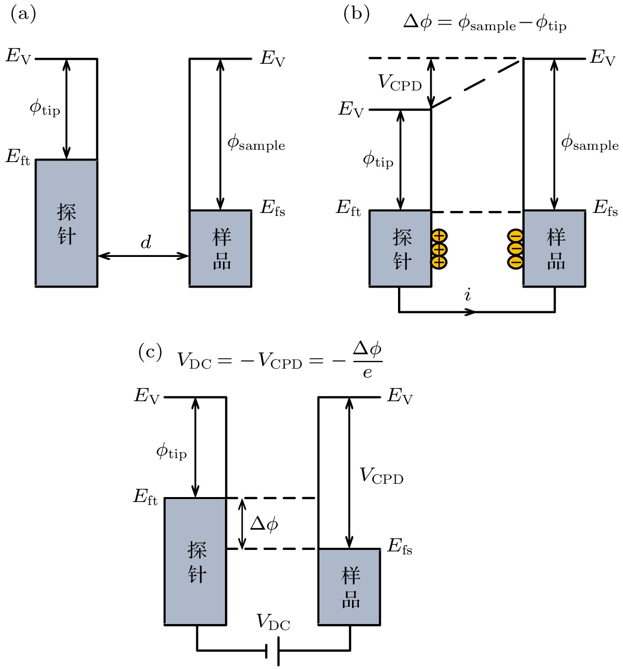
图 1 样品和AFM探针之间电子能级的三种示意图 (a) 尖端和样品分开距离d没有电接触; (b) 尖端和样品电接触; (c) 施加外部偏压
$ {V}_{\mathrm{D}\mathrm{C}} $ 于尖端和样品之间以抵消接触区域的静电力CPD,$ {E}_{\mathrm{V}} $ 是真空能级,$ {E}_{\mathrm{f}\mathrm{s}} $ 和$ {E}_{\mathrm{f}\mathrm{t}} $ 分别为样品和尖端的费米能级Figure 1. Three schematic diagrams of electron energy levels between sample and AFM probe: (a) No electrical contact between tip and sample separation distance d; (b) electrical contact between tip and sample; (c) apply an external bias
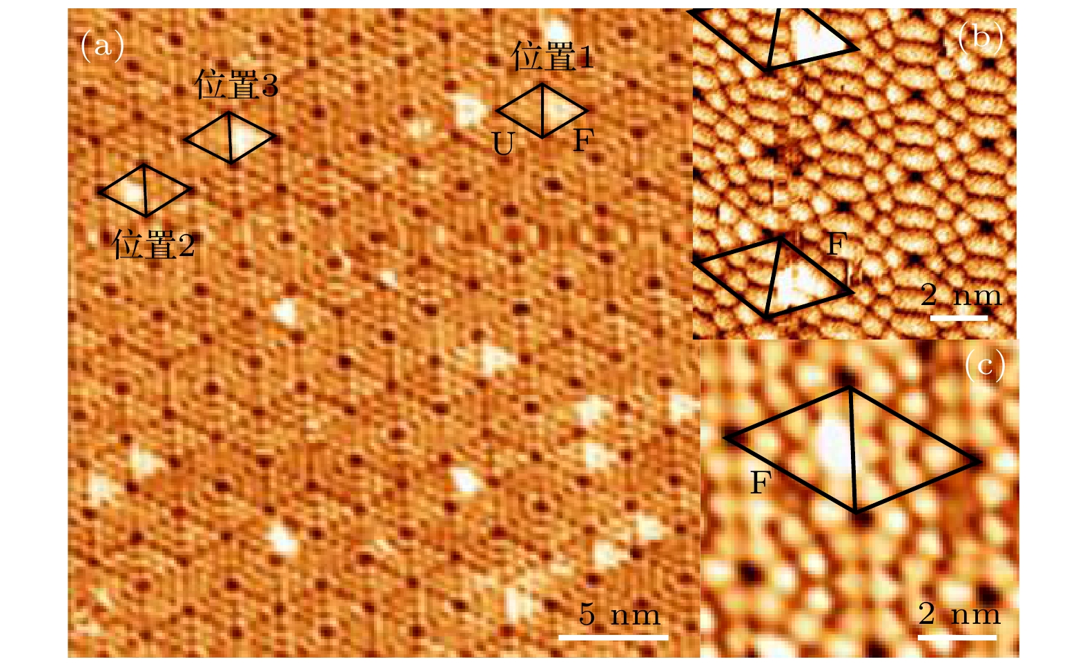
$ {V}_{\mathrm{D}\mathrm{C}} $ to counteract the electrostatic force CPD in the contact area between the tip and the sample.$ {E}_{\mathrm{V}} $ is the vacuum level,$ {E}_{\mathrm{f}\mathrm{s}} $ and$ {E}_{\mathrm{f}\mathrm{t}} $ is the Fermi level of the sample and the tip, respectively.图 4 吸附在Si(111)-(7×7)表面Au原子的AFM图像 (a) 成像尺寸为40 nm×40 nm, 设定值
$ \Delta f $ = 25 Hz; (b) 成像尺寸为10 nm×10 nm, 设定值$ \Delta f $ = 33 Hz; (c) 成像尺寸为5 nm×5 nm, 设定值$ \Delta f $ = 45 Hz. 用探针分别观察到Si(111)-(7×7)表面上的Au原子是较亮的突起. 成像参数为悬臂的共振频率f0 = 160.288 kHz, 振荡幅值A = 7 nm, 悬臂的弹性系数k = 45 N/m, 在样品上施加的直流偏置电压VBias = 120 mV, 恒定频率模式Figure 4. AFM images of Au atom adsorbed on the surface of Si (111)-(7×7), respectively: (a) Imaging size of 40 nm×40 nm, the set point of
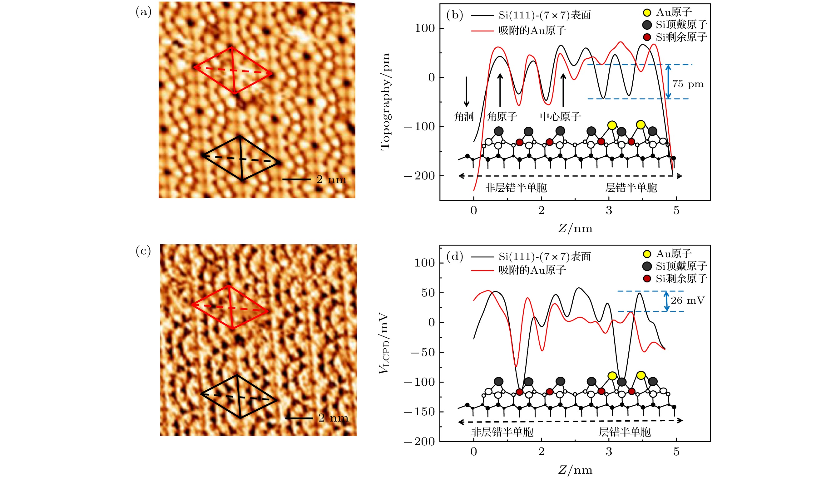
$ \Delta f $ = 25 Hz; (b) imaging size of 10 nm×10 nm, the set point of$ \Delta f $ = 33 Hz; (c) imaging size of 5 nm×5 nm, the set point of$ \Delta f $ = 25 Hz. The Au atom on the Si (111)-(7×7) surface are bright protrusions observed by probes. Imaging parameters: the resonance frequency of the cantilever is${f}_{0}=160.288\;\mathrm{k}\mathrm{H}\mathrm{z}$ , the oscillation amplitude is A = 7 nm, the elasticity coefficient of the cantilever is k = 45 N/m, the DC bias voltage applied on the sample is$ {V}_{\mathrm{B}\mathrm{i}\mathrm{a}\mathrm{s}} $ = 120 mV, constant frequency mode.图 5 (a) 吸附在Si(111)-(7×7)表面的Au原子的AFM图像; (c) Au原子吸附在Si(111)-(7×7)表面的LCPD图像. 成像参数: 悬臂的共振频率
${f}_{0}=165.348\;\mathrm{k}\mathrm{H}\mathrm{z}$ , 振荡幅值A = 7 nm, 悬臂的弹性系数为k = 45 N/m, 恒定频率模式, 直流偏置电压$ {V}_{\mathrm{B}\mathrm{i}\mathrm{a}\mathrm{s}} $ = 78 mV, 设定值$ \Delta f $ = 43 Hz; KPFM控制器参数为$ {V}_{\mathrm{A}\mathrm{C}} $ = 0.5 V,$ {f}_{\mathrm{A}\mathrm{C}} $ = 0.5 kHz; (b), (d) 吸附的Au原子的AFM和LCPD谱线Figure 5. (a) AFM images of the Au atom adsorbed on the Si(111)-(7×7) surfaces; (c) LCPD images of the Au atom adsorbed on the Si (111)-(7×7) surfaces. Imaging parameters: resonance frequency
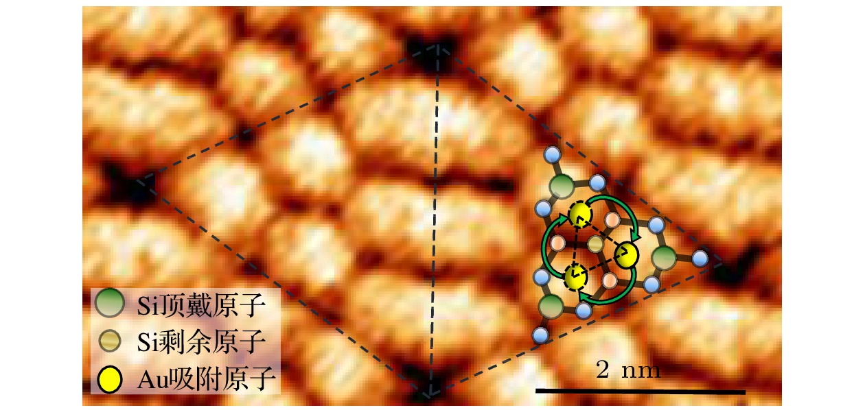
${f}_{0}=165.348\;\mathrm{k}\mathrm{H}\mathrm{z}$ , oscillation amplitude A = 7 nm, elasticity coefficient k = 45 N/m, constant frequency mode, DC bias voltage$ {V}_{\mathrm{B}\mathrm{i}\mathrm{a}\mathrm{s}} $ = 78 mV, the set point of$ \Delta f $ = 43 Hz; KPFM controller parameters are$ {V}_{\mathrm{A}\mathrm{C}} $ = 0.5 V,$ {f}_{\mathrm{A}\mathrm{C}} $ = 0.5 kHz; (b), (d) the AFM and LCPD spectral lines of the adsorbed Au atom.图 7 单个Au原子吸附Si(111)-(7×7)表面的三角形不定域吸附特征形成原理, 图中为一个菱形单元. 虚线圈表示Au在该吸附位点一直来回移动, 形成不定域吸附特征. 成像尺寸为5 nm × 3 nm
Figure 7. Formation principle of adsorption characteristics about triangular delocalized adsorption of single Au atom adsorbed on Si surface, in the figure, a diamond unit is shown. The dotted line circle indicates that Au has been moving back and forth at this adsorption site, and forming the adsorption characteristic of delocalized adsorption. Imaging size: 5 nm × 3 nm.
图 8 Au原子吸附在Si(111)-(7×7)不同位置的差分电荷密度分布 (a) Au原子吸附在Si顶戴原子位置, Au—SiA键长为2.3 Å; (b) Au原子吸附在Si剩余原子的位置, Au—SiR键长为2.29 Å; (c) Au原子吸附在Si(111)-(7×7)表面的高配位, Au—Si键长为2.51 Å. 图中红色部分表示该位置电荷减少, 蓝色部分表示电荷的增加
Figure 8. Differential charge density distribution of Au atom adsorbed at different positions of Si(111)-(7×7), respectively: (a) Au atom adsorbed at the position of Si adatom, and the bond length of Au—SiA is 2.3 Å; (b) the position of Au atom adsorbed on the Si rest atom, and the bond length of Au—SiR is 2.29 Å; (c) the high coordination of Au atom adsorbed on the Si(111)-(7×7) surface, and the Au—Si bond length is 2.51 Å. In the figure, the red part indicates the decrease of charge at this position, and the blue part indicates the increase of charge.
图 9 Au原子未吸附时与吸附在Si(111)-(7×7)最佳位置的差分电荷密度分布 (a) Au原子未吸附在Si表面原子位置; (b) Au原子吸附在Si(111)-(7×7)表面的高配位. 黑色虚线三角框表示一个菱形半单胞中的盆地区域. 图中红色部分表示该位置电荷减少, 蓝色部分表示电荷的增加
Figure 9. Differential charge density distribution of Au atom not adsorbed and the best position adsorbed on Si(111)-(7×7): (a) The atomic position of Au atom not adsorbed on Si surface; (b) the high coordination of Au atom adsorbed on the surface of Si(111)-(7×7). The black dotted triangular box represents the basin area in a HUC. In the figure, the red part indicates the decrease of charge at this position, and the blue part indicates the increase of charge.
-
[1] Zou S R, Sugawara Y, Li Y J 2021 J. Phys. Chem. C 125 446
 Google Scholar
[2] Wang H W, Lu J L 2020 Chin. J. Chem. 38 1422
 Google Scholar
[3] Qu B, Hu J H, Li H, Li W J, Huang M L, Wu Q H 2015 Surf. Interface Anal. 47 926
 Google Scholar
[4] Sonnet P, Stauffer L, Minot C 1998 Surf. Sci. 402 751
 Google Scholar
[5] Li Y J, Takeuchi O, Don N. Futaba, Oigawa H, Miyake K, Shigekawa H 2003 Phys. Rev. B 68 033301
 Google Scholar
[6] Chen G, Xiao X D, Kawazoe Y, Gong X G, Chan C T 2009 Phys. Rev. B 79 115301
 Google Scholar
[7] Zhang C, Chen G, Wang K D, Yang H W, Su T, Chan C T, Loy M M T, Xiao X D 2005 Phys. Rev. Lett. 94 176104
 Google Scholar
[8] Zhang L, Jeon Y J, Shim H, Lee G 2012 J. Vac. Sci. Technol. , A 30 61406
 Google Scholar
[9] 李彦, 郑琦, 常霄, 黄立, 林晓, 程志海, 高鸿钧 2021 70 136802
 Google Scholar
Li Y, Zheng Q, Chang X, Huang L, Lin X, Cheng Z H, Gao H J 2021 Acta Phys. Sin. 70 136802
 Google Scholar
[10] Melitz W, Shen J, Kummel A C, Lee S 2011 Surf. Sci. Rep. 66 1
 Google Scholar
[11] Wandelt K 1997 Appl. Surf. Sci. 111 1
 Google Scholar
[12] Castañeda-Uribe O A, Avila A, Reifenberger R, and Raman A 2015 ACS Nano. 9 2938
 Google Scholar
[13] Zou S R, Yokoyama H, Sugawara Y, Li Y J 2020 J. Phys. Chem. C 124 21641
 Google Scholar
[14] Adachi Y, Wen H F, Zhang Q Z, Miyazaki M, Sugawaraa Y, Li Y J 2020 Nanoscale Adv. 2 2371
 Google Scholar
[15] 温焕飞, 菅原康弘, 李艳君 2020 69 210701
 Google Scholar
Wen H F, Sugawara Y, Li Y J 2020 Acta Phys. Sin. 69 210701
 Google Scholar
[16] Miyazaki M, Wen H F, Zhang Q Z, Adachi Y, Brndiar J, Štich Ivan, Li Y J, Sugawara Y 2019 Beilstein J. Nanotechnol. 10 1228
 Google Scholar
[17] Faliya K, Kliem H, Dias C J 2017 IEEE Trans Dielectr. Electr. Insul. 24 1913
 Google Scholar
[18] Gross L, Mohn F, Liljeroth P, Repp J, Giessibl F J, Meyer G 2009 Science 324 1428
 Google Scholar
[19] Liu Q, Fu Q, Shao X J, Ma X H, Wu X F, Wang K D, Xiao X D 2017 Appl. Surf. Sci. 401 225
 Google Scholar
[20] Sadewasser S, Jelinek P, Fang C K, Custance O, Yamada Y, Sugimoto Y, Abe M, Morita S 2009 Phys. Rev. Lett. 103 266103
 Google Scholar
[21] Kinoshita Y, Naitoh Y, Li Y J, Sugawara Y 2011 Rev. Sci. Instrum. 82 113707
 Google Scholar
[22] Li Y J, Wen H F, Zhang Q, Adachi Y, Arima E, Kinoshita Y, Nomura H, Ma Z, Kou L, Tsukuda Y, Naitoh Y, Sugawara Y, Xu R, Cheng Z H 2018 Ultramicroscopy 191 51
 Google Scholar
[23] Cho K, Kaxiras E 1998 Surf. Sci. 396 L261
 Google Scholar
[24] Zhou Y H, Wu Q H, Li S P, Kang J Y 2007 Surf. Rev. Lett. 14 657
 Google Scholar
Catalog
Metrics
- Abstract views: 7635
- PDF Downloads: 129
- Cited By: 0




 DownLoad:

