


-
Two-dimensional (2D) niobium silicon telluride (Nb2SiTe4) was recently proposed as a promising candidate in infrared detector, photoelectric conversion, polarized optical sensor and ferroelastic switching application due to its narrow bandgap, long-term air stability, high carrier mobility, etc. However, the in-plane strains and interfacial defects induced by the lattice misfits between functional layers are harmful to 2D heterojunction nanodevice performance, making the crystal-lattice regulation and strain engineering necessary to achieve lattice matching and strain-controllable interface. Here, using first-principles calculations and elemental substitutions, i.e., replacing cations (anions) with elements in the same group of periodic table, we identify three new and stable single-layer A2BX4 analogues (Nb2SiSe4, Nb2SnTe4 and Ta2GeTe4) as appealing candidates in manipulating the lattice parameters of Nb2SiTe4. The controllable lattice parameters are 6.04 Å ≤ a ≤ 6.81 Å and 7.74 Å ≤ b ≤ 8.15 Å. Among them, Ta2GeTe4 exhibits similar lattice parameters to Nb2SiTe4 but smaller bandgap, yielding better response in far-infrared region. Strain engineering shows that the external biaxial tensile stress narrows the bandgaps of A2BX4 due to the downshifting in energy of conduction band minimum (CBM). External biaxial compressive stress induces valance band maximum (VBM) orbital inversion for Nb2SiTe4, Nb2GeTe4 and Ta2GeTe4, which pushes up VBM and discontinues the trend of corresponding bandgap increase. In this case, the bandgap change depends on the competition between energy upshifts of both CBM and VBM. In the Nb2SiSe4 and Nb2SnTe4 cases, the d-p antibonding coupling in valance band is so strong that no valance band inversion appears while the bandgap increases by ~0.3 eV under −5% compressive strain. Regarding Nb2SiTe4, Nb2GeTe4 and Ta2GeTe4, their bandgaps can hardly change under −5% compressive strain, indicating that the energy upshift in VBM equals that in CBM. Such a valance band inversion is attributed to Te outmost p orbital overlapping, which introduces more dispersive VBM and smaller effective mass of hole. Our findings suggest that Nb2SiTe4 can be alloyed with Nb2SiSe4, Nb2SnTe4 and Ta2GeTe4 to achieve controllable device lattice matching while maintaining its superior properties at the same time. The use of external biaxial compressive stress can promote the hole diffusion and improve the device performance.
[1] Novoselov K S, Geim A K, Morozov S V, Jiang D, Zhang Y, Dubonos S V, Grigorieva I V, Firsov A A 2004 Science 306 666
 Google Scholar
[2] Fan Y, Liu X, Wang J, Ai H, Zhao M 2018 Phys. Chem. Chem. Phys. 20 11369
Google Scholar
[3] Son Y W, Cohen M L, Louie S G 2006 Phys. Rev. Lett. 97 216803
Google Scholar
[4] Qiao Z, Ren W, Chen H, Bellaiche L, Zhang Z, Macdonald A H, Niu Q 2014 Phys. Rev. Lett. 112 116404
Google Scholar
[5] Ishii T, Sato T 1983 J. Cryst. Growth 61 689
Google Scholar
[6] Radisavljevic B, Radenovic A, Brivio J, Giacometti V, Kis A 2011 Nat. Nanotechnol. 6 147
Google Scholar
[7] Qiao J, Kong X, Hu Z X, Yang F, Ji W 2014 Nat. Commun. 5 4475
Google Scholar
[8] Venkatasubramanian R, Colpitts T, Watko E, Lamvik M, El-Masry N 1997 J. Cryst. Growth 170 817
Google Scholar
[9] Zhao M, Xia W, Wang Y, Luo M, Tian Z, Guo Y, Hu W, Xue J 2019 ACS Nano 13 10705
Google Scholar
[10] Fang W Y, Li P A, Yuan J H, Xue K H, Wang J F 2019 J. Electron. Mater. 49 959
Google Scholar
[11] Zhang T, Ma Y, Xu X, Lei C, Huang B, Dai Y 2020 J. Phys. Chem. Lett. 11 497
Google Scholar
[12] Jain S C, Harker A H, Cowley R A 1997 Philos. Mag. A 75 1461
Google Scholar
[13] Wosinski T, Yastrubchak O, Makosa A, Figielski T 2000 J. Phys. Condens. Matter 12 10153
Google Scholar
[14] Smith A M, Mohs A M, Nie S 2009 Nat. Nanotechnol. 4 56
Google Scholar
[15] Perdew J P, Burke K, Ernzerhof M 1996 Phys. Rev. Lett. 77 3865
Google Scholar
[16] Kresse G, Joubert D 1999 Phys. Rev. B 59 1758
Google Scholar
[17] Monkhorst H J, Pack J D 1976 Phys. Rev. B 13 5188
Google Scholar
[18] Heyd J, Scuseria G E, Ernzerhof M 2003 J. Chem. Phys. 118 8207
Google Scholar
[19] Togo A, Tanaka I 2015 Scr. Mater. 108 1
Google Scholar
[20] Jain A, Ong S P, Hautier G, Chen W, Richards W D, Dacek S, Cholia S, Gunter D, Skinner D, Ceder G, Persson K A 2013 APL Mater. 1 011002
Google Scholar
[21] Tremel W, Kleinke H, Derstroff V, Reisner C 1995 J. Alloys. Compd. 219 73
Google Scholar
[22] Gareh J, Boucher F, Evain M 1996 Eur. J. Solid State Inorg. Chem. 33 355
[23] Snyder G J, Caillat T, Fleurial J P 2011 J. Mater. Res. 15 2789
Google Scholar
-
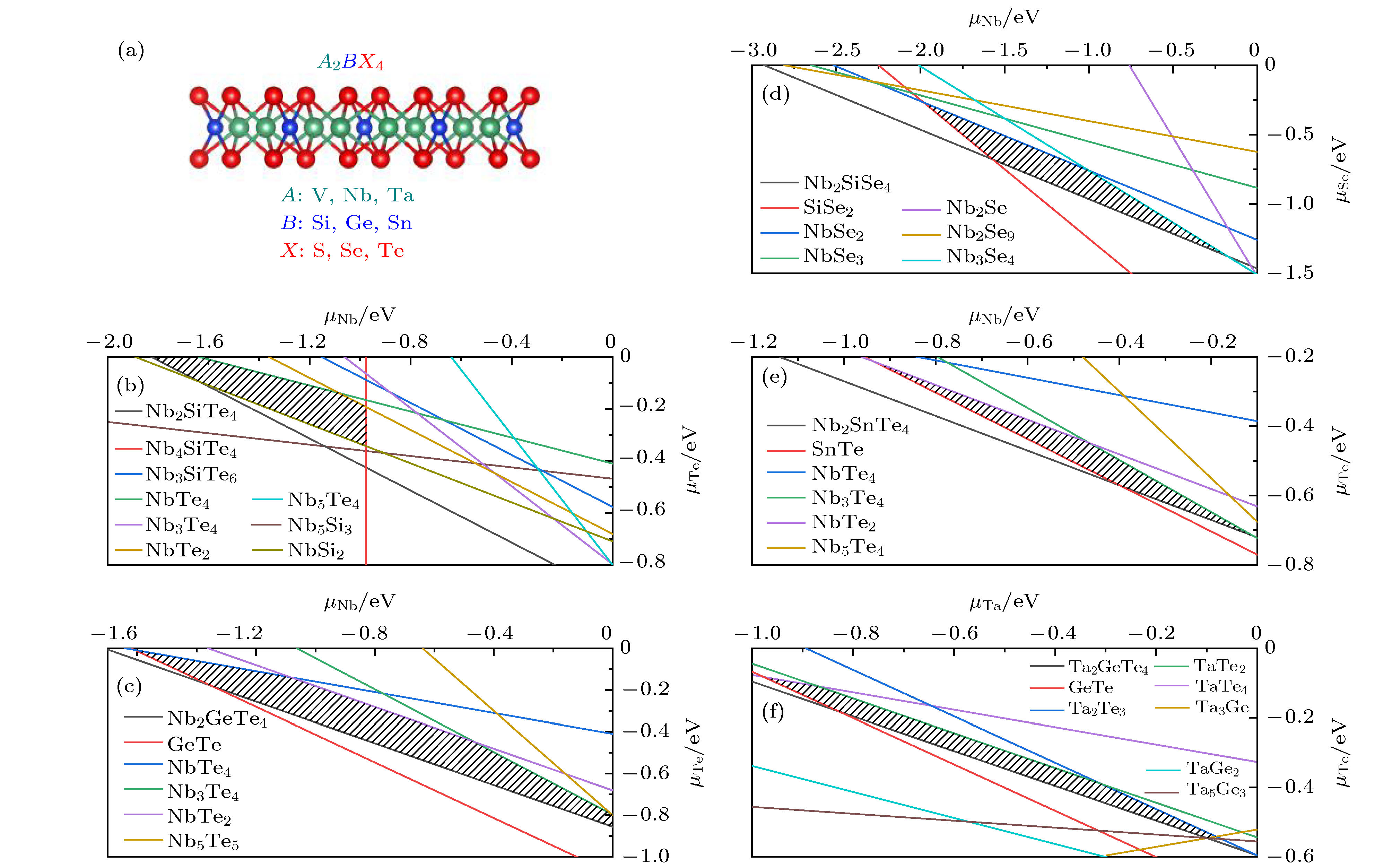
图 1 (a) 二维A2BX4化合物的晶体结构图; (b)—(f) 筛选出的5种稳定A2BX4化合物的化学势能窗口图, 分别对应Nb2SiTe4, Nb2GeTe4, Nb2SiSe4, Nb2SnTe4和Ta2GeTe4.
Figure 1. (a) Crystal structure of A2BX4 compounds; (b)–(f) Chemical potential windows for 5 stable A2BX4 compounds corresponding to Nb2SiTe4, Nb2GeTe4, Nb2SiSe4, Nb2SnTe4 and Ta2GeTe4, respectively.
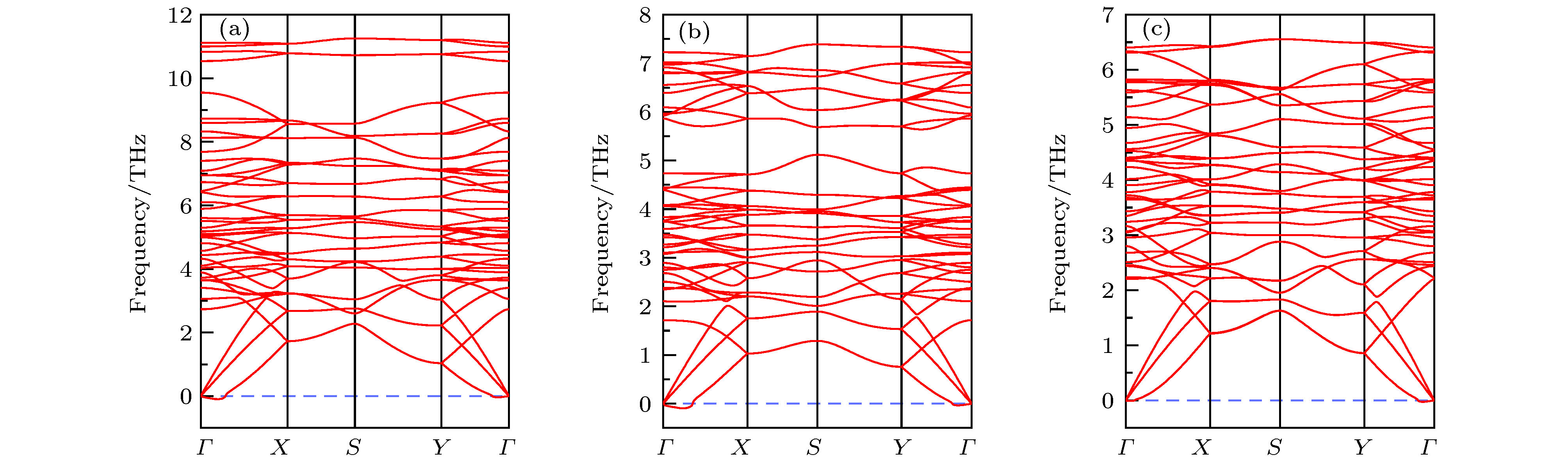
图 2 0 K下基于PBE计算的声子谱 (a) Nb2SiSe4; (b) Nb2SnTe4; (c) Ta2GeTe4
Figure 2. PBE calculated phonon dispersions for (a) Nb2SiSe4, (b) Nb2SnTe4 and (c) Ta2GeTe4 under 0 K.

图 3 HSE06计算的能带结构 (a) Nb2SiSe4; (b) Nb2SiTe4; (c) Nb2GeTe4; (d) Nb2SnTe4; (e) Ta2GeTe4. 其中蓝线(绿线)代表Nb2SiTe4的VBM(CBM)位置, 数字表示相比Nb2SiTe4 VBM(CBM)的移动
Figure 3. HSE06 calculated band structures for (a) Nb2SiSe4, (b) Nb2SiTe4, (c) Nb2GeTe4, (d) Nb2SnTe4 and (e) Ta2GeTe4, respectively. Lines represent for VBM (blue) and CBM (green) of Nb2SiTe4. Numbers indicate VBM(CBM) shifts compared with Nb2SiTe4.
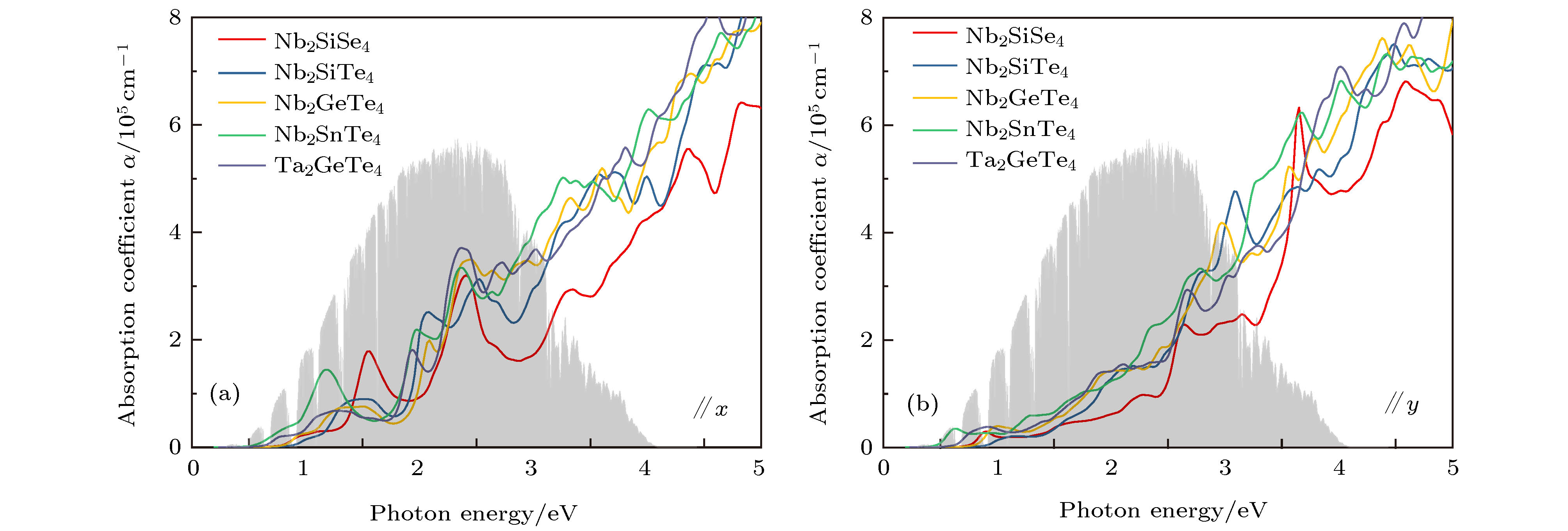
图 4 计算的5种A2BX4光吸收谱 (a) 沿x方向; (b) 沿y方向
Figure 4. Calculated optical absorption coefficients for five A2BX4 compounds along (a) x direction and (b) y directions.

图 5 PBE计算的外加 ± 5%应力时A2BX4的能带结构图 (a) Nb2SiSe4; (b) Nb2SiTe4; (c) Nb2GeTe4; (d) Nb2SnTe4; (e) Ta2GeTe4; (f), (g), (h)为对应外应力下Nb2SiTe4 VBM的电荷密度图
Figure 5. PBE calculated band structures for A2BX4 under ± 5% strain: (a) Nb2SiSe4; (b) Nb2SiTe4; (c) Nb2GeTe4; (d) Nb2SnTe4; (e) Ta2GeTe4; (f), (g), (h) VBM charge density maps of Nb2SiTe4 under strains.
表 1 A2BX4化合物的理论晶格常数与带隙值
Table 1. Theoretical lattice constants and bandgaps of stable A2BX4 compounds.
 DownLoad: CSV
-
[1] Novoselov K S, Geim A K, Morozov S V, Jiang D, Zhang Y, Dubonos S V, Grigorieva I V, Firsov A A 2004 Science 306 666
Google Scholar
[2] Fan Y, Liu X, Wang J, Ai H, Zhao M 2018 Phys. Chem. Chem. Phys. 20 11369
Google Scholar
[3] Son Y W, Cohen M L, Louie S G 2006 Phys. Rev. Lett. 97 216803
Google Scholar
[4] Qiao Z, Ren W, Chen H, Bellaiche L, Zhang Z, Macdonald A H, Niu Q 2014 Phys. Rev. Lett. 112 116404
Google Scholar
[5] Ishii T, Sato T 1983 J. Cryst. Growth 61 689
Google Scholar
[6] Radisavljevic B, Radenovic A, Brivio J, Giacometti V, Kis A 2011 Nat. Nanotechnol. 6 147
Google Scholar
[7] Qiao J, Kong X, Hu Z X, Yang F, Ji W 2014 Nat. Commun. 5 4475
Google Scholar
[8] Venkatasubramanian R, Colpitts T, Watko E, Lamvik M, El-Masry N 1997 J. Cryst. Growth 170 817
Google Scholar
[9] Zhao M, Xia W, Wang Y, Luo M, Tian Z, Guo Y, Hu W, Xue J 2019 ACS Nano 13 10705
Google Scholar
[10] Fang W Y, Li P A, Yuan J H, Xue K H, Wang J F 2019 J. Electron. Mater. 49 959
Google Scholar
[11] Zhang T, Ma Y, Xu X, Lei C, Huang B, Dai Y 2020 J. Phys. Chem. Lett. 11 497
Google Scholar
[12] Jain S C, Harker A H, Cowley R A 1997 Philos. Mag. A 75 1461
Google Scholar
[13] Wosinski T, Yastrubchak O, Makosa A, Figielski T 2000 J. Phys. Condens. Matter 12 10153
Google Scholar
[14] Smith A M, Mohs A M, Nie S 2009 Nat. Nanotechnol. 4 56
Google Scholar
[15] Perdew J P, Burke K, Ernzerhof M 1996 Phys. Rev. Lett. 77 3865
Google Scholar
[16] Kresse G, Joubert D 1999 Phys. Rev. B 59 1758
Google Scholar
[17] Monkhorst H J, Pack J D 1976 Phys. Rev. B 13 5188
Google Scholar
[18] Heyd J, Scuseria G E, Ernzerhof M 2003 J. Chem. Phys. 118 8207
Google Scholar
[19] Togo A, Tanaka I 2015 Scr. Mater. 108 1
Google Scholar
[20] Jain A, Ong S P, Hautier G, Chen W, Richards W D, Dacek S, Cholia S, Gunter D, Skinner D, Ceder G, Persson K A 2013 APL Mater. 1 011002
Google Scholar
[21] Tremel W, Kleinke H, Derstroff V, Reisner C 1995 J. Alloys. Compd. 219 73
Google Scholar
[22] Gareh J, Boucher F, Evain M 1996 Eur. J. Solid State Inorg. Chem. 33 355
[23] Snyder G J, Caillat T, Fleurial J P 2011 J. Mater. Res. 15 2789
Google Scholar


 DownLoad:


Catalog
Metrics
- Abstract views: 11078
- PDF Downloads: 309
- Cited By: 0
