-
光电产额谱的实验和理论研究对所有涉及光电的材料和器件都很重要, 其中能够准确地从入射光子能量计算光电产额对最大限度地从光电产额谱获取光电材料和器件的电性能的微观信息至关重要. 本文在建立起光电产额谱满足的微分方程结合光电产额谱的特有实验结果之后找到了这个满足光电产额谱的特有实验结果下微分方程的解. 通过对实验数据进行最小二乘法非线性拟合既验证了这种方法获得的光电产额谱模型的正确性, 也得到了每一条光电产额谱的具体数学表达. 应用此模型不仅能尽可能精确可靠地计算出两种电性能略有不同的物质相互接触形成结的势垒高度, 而且由这个光电产额谱模型能够得到在结中的电子有效占有态的密度能级分布.Experimental and theoretical research on photoelectron yield spectrum play a crucial role in electronic and photo-electronic materials and devices, and the reliable and precise estimation of photoelectron yield via photon energy is very important for detecting microscopic electrical information in photo-electronic materials and devices. Photoelectron yield is defined as the number of electrons emitted by per incident photon. Before this work, the technique was based on the interception of a plot of square root of photoelectron yield versus photon energy for metal-insulator hetero-junction, and that of a plot of cube root of photoelectron yield variation with photon energy for insulator-semiconductor hetero-junction. But, how to intercept the relationship between photoelectron yield and photon energy for semiconductor-semiconductor and metal-semiconductor hetero-junctions has not been known. Besides, many experimental plots of square root and cube root of photoelectron yield against photon energy are available, but none of them is a straight line. In order to obtain a more accurate and reliable barrier height, electrical structure of the junction, the energy level distribution of the energy band offset, defect density in the junction, and the valence band profile through the photoelectric yield spectrum, a reliable and accurate model of photoelectron yield spectrum is established via combining the solution to a differential equation and experimental results. A method is proposed to naturally determine the junction barrier height by using the experimental results of the internal current yield varying with the photon energy. The this method can be used to calculate the junction barrier height as accurately and reliably as possible, and the density and energy level distributions of the effective occupancy states of the electrons in the four junctions are obtained by using this photoelectric yield spectrum model, In addition, based on this model, this paper proves mathematically that the density and energy level distribution of the effective occupancy state of electrons present a peak shape. Therefore, the application prospects of this photoelectric yield spectrum model are demonstrated.
-
Keywords:
- photoelectron yield spectroscopy /
- photonic energy /
- model /
- junction barrier height
[1] Hertz H 1887 Ann. Phys. 31 983
[2] Einstein A 1905 Ann. Phys. 322 132
 Google Scholar
[3] Millikan R 1916 Phys. Rev. 7 18
 Google Scholar
[4] Fowler R H 1931 Phys. Rev. 38 45
 Google Scholar
[5] Liu C, Liu W L 2018 Optik 154 726
 Google Scholar
[6] Herbert B M 1977 J. Appl. Phys. 48 4729
 Google Scholar
[7] Chapin D M, Fuller C S, Pearson G L 1954 J. Appl. Phys. 25 676
 Google Scholar
[8] Hanae T, Yousaf H K, Faisal B, Bernabe M S, Mohamed E T 2019 Sol. Energy 194 932
 Google Scholar
[9] Daisuke Y, Tsuyoshi Y, So N, Tomoyuki Y 2012 Phys. B 407 4485
 Google Scholar
[10] Kun X, Caifu Z, Qin Z, Peide Y, Kang W, Curt A R, David G, Nhan V N 2012 70th Device Research Conference DOI: 10.1109/DRC.2012.6256941
[11] Afanas’ev V V, Chou H Y A, Stesmans C, Merckling X S 2011 Microelectron. Eng. 88 1050
 Google Scholar
[12] Akio O, Mitsuhisa I, Katsunori M, Seiichi M 2017 Microelectron. Eng. 17825 85
[13] Kolomiiets N M, Afanas’ev V V, Jayachandran S, Delabie A, Heyns M, Stesmans A 2016 ECS J. Solid State Sci. Technol. 5 3008
[14] Jenkins M A, McGlone J M, Wager J F, Conley J F J 2019 J. Appl. Phys. 125 055301
 Google Scholar
[15] Sang Y L, Jaewan C, Jaehyung C, Younsoo K, HanJin L, Hyeongtag J, Hyungtak S 2017 Curr. Appl. Phys. 17 267
 Google Scholar
[16] Shlyakhov J, Chai M, Yang S J, Wang V V, Afanas’ev M, Houssa A Stesmans 2018 Apl. Materials 6 026801
 Google Scholar
[17] Melanie A J, Tyler K, Dustin Z A, Wei L, Nhan V N, John F, Conley J 2018 Phys. Status Solidi RRL 12 1700437
 Google Scholar
[18] John F G, Myles A S, Nikhil J, Kevin L, Schulte R M F, William E, McMahon E E, Perl D J F 2018 IEEE J. photovoltaics 8 626
 Google Scholar
[19] Vadim T, Inge A, Steven B, Cedric H, Iuliana R, Afanas'ev, V, Michel H, Andre S 2019 Thin Solid Films 674 39
 Google Scholar
[20] Shalish L, Kronik G S, Yoram S, Eizenberg M 2000 Appl. Phys. Lett. 77 987
 Google Scholar
[21] Seber G A F, Wild J 2003 Nonlinear Regression (New Jersey: John Wiley & Sons, Inc.) p355
[22] Almeida J, Tiziana D, Coluzza C, Margaritondo G, Bergossi O, Spajer M, Courjon D 1996 Appl. Phys. Lett. 69 2361
 Google Scholar
[23] Shi J L, Ang L K 2015 Phys. Rev. Appl. 3014002
[24] Isao S, Mitsuyuki Y, Hitoshi K 2009 Sol. Energy Mater. Sol. Cells 93 737
 Google Scholar
[25] Carsten D, Daniel M, Julien G 2010 Phys. Rev. B 81 085202
 Google Scholar
[26] Liu C, Li F 2012 Opt. Commun. 285 2868
 Google Scholar
[27] Liu C S 2020 Polym. Test. 91 106686
 Google Scholar
[28] Szijber J 1987 J. Electron Spectrosc. Relat. Phenom. 43 113
 Google Scholar
[29] Ammar S, Bogdan J, Kowalski E, Nehme A K 2007 J. Electron Spectrosc. Relat. Phenom. 160 58
 Google Scholar
-
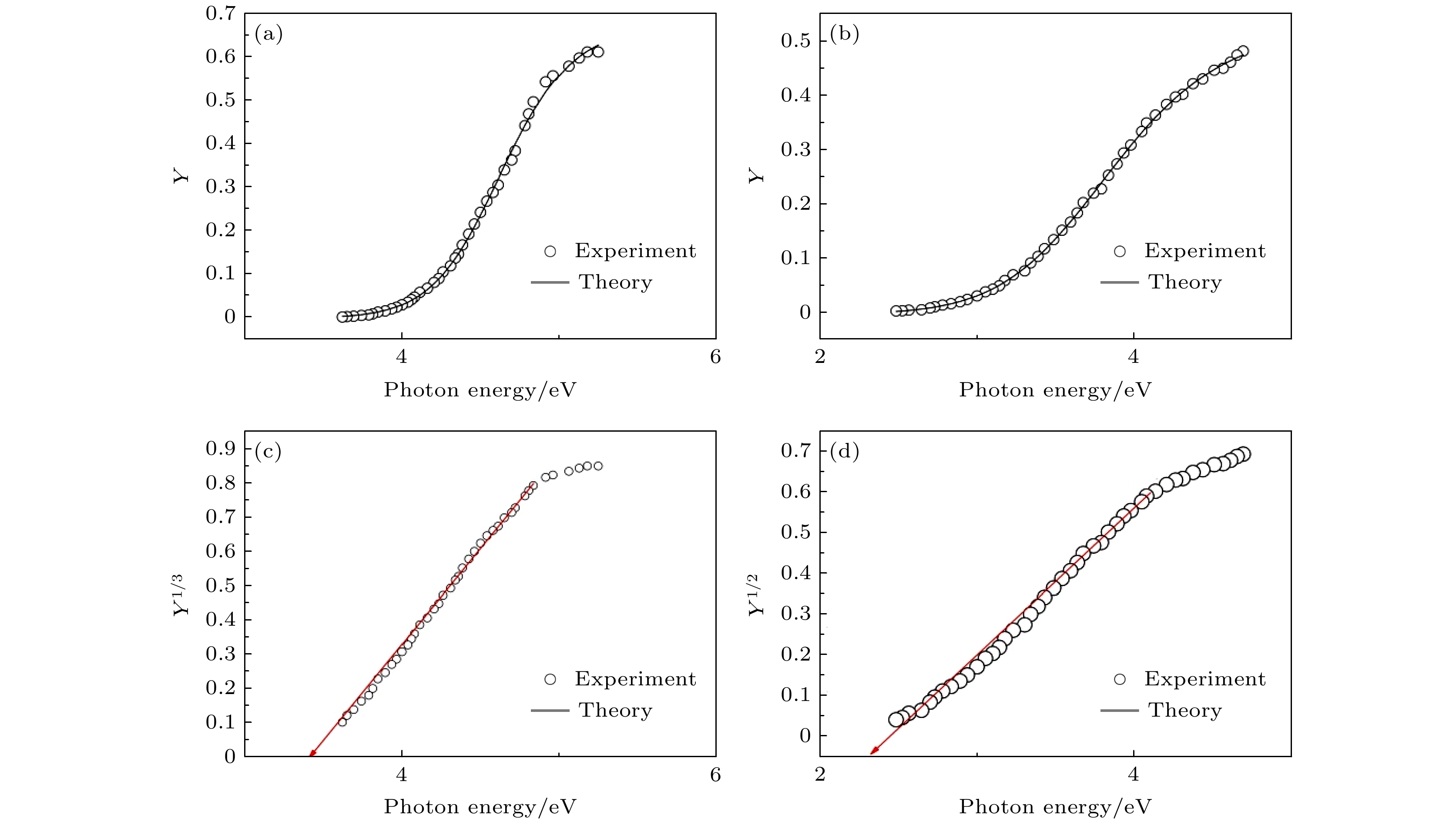
图 2 实验和模型(6)模拟的Al0.2Ga0.3In0.5P/Al0.2Ga0.8As(半导体-半导体 (a), (c))和Pt/GaP(金属-半导体, (b), (d))异质结内光电产额(Y)作为入射光能量函数的结果及Y1/3和Y1/2随入射光能量变化图
Fig. 2.
$\sqrt[n]{Y} \text- h\nu$ and$Y \text- h\nu$ plots of the experimental data and the theoretical fits in the form of Eq. (6) for both Al0.2Ga0.3In.5P/Al0.2Ga0.8As ((a), (c)) and Pt/GaP ((b), (d)) Schottky contacts.图 3 实验和模型(6)模拟的石墨烯/二氧化硅(Graphene/SiO2 (c), (d)), p型单晶硅(b)和有机半导体P3HT(a)光电产额(Y)作为入射光能量函数的结果及Y1/3随入射光能量变化图
Fig. 3. Experimental and theoretical IPE yield as a function of photon energy for Graphene/SiO2 ((c), (d)), P3HT (a) and p-type Si (b).
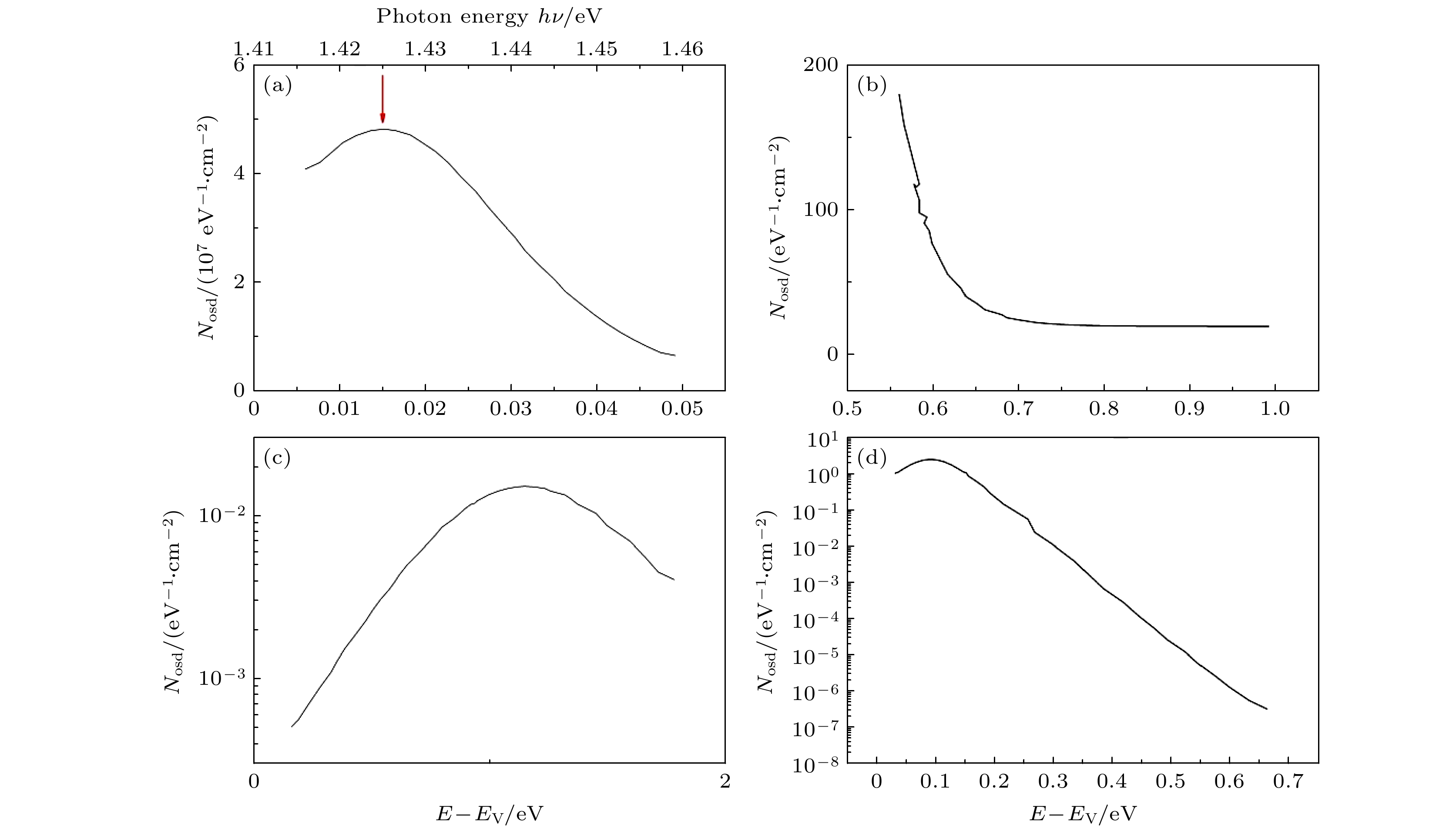
图 4 Pt/GaP (a), Al0.2Ga0.3In0.5P/Al0.2Ga0.8As (b), MoS2/SiO2 (c)和P3HT(d)电子有效占有态的密度按照能级(能量)分布
Fig. 4. Curves display the spectra of the effective density of the filled electronic states of the Pt/GaP (a), Al0.2Ga0.3In0.5P/Al0.2Ga0.8As (b), MoS2/SiO2 (c) and P3HT (d), as the first derivative of the recorded.
表 1 不同结中的优化参数和评价参数取值以及获得的势垒高度
Table 1. The best parameters and evaluation parameters for different junctions, and calculated barrier height.
结 Ysat Ymin $h{\nu _1}$ k R ARE/% φ/eV MoS2/SiO2 .68 –.0017 4.63 20.58 .999 2.3 3.46 HfO2/ ZCAN .53 –.0038 3.86 10.68 .999 1.5 2.43 Al.2Ga.3In.5P/Al.2Ga.8As .90 –4477.06 1.78 55.14 .999 3.4 1.52 单晶Si .39 –.0094 1.72 9.05 .998 3.8 1.14 P3HT .14 –.0066 1.94 67.82 .999 1.2 1.85 Graphene/SiO2 .22 –.049 4.75 26.94 .999 4.1 4.12 Pt/GaP .87 –.37 1.43 142.86 .999 3.7 1.41 R: 相关系数, ARE: 相对误差的平均值. -
[1] Hertz H 1887 Ann. Phys. 31 983
[2] Einstein A 1905 Ann. Phys. 322 132
 Google Scholar
[3] Millikan R 1916 Phys. Rev. 7 18
 Google Scholar
[4] Fowler R H 1931 Phys. Rev. 38 45
 Google Scholar
[5] Liu C, Liu W L 2018 Optik 154 726
 Google Scholar
[6] Herbert B M 1977 J. Appl. Phys. 48 4729
 Google Scholar
[7] Chapin D M, Fuller C S, Pearson G L 1954 J. Appl. Phys. 25 676
 Google Scholar
[8] Hanae T, Yousaf H K, Faisal B, Bernabe M S, Mohamed E T 2019 Sol. Energy 194 932
 Google Scholar
[9] Daisuke Y, Tsuyoshi Y, So N, Tomoyuki Y 2012 Phys. B 407 4485
 Google Scholar
[10] Kun X, Caifu Z, Qin Z, Peide Y, Kang W, Curt A R, David G, Nhan V N 2012 70th Device Research Conference DOI: 10.1109/DRC.2012.6256941
[11] Afanas’ev V V, Chou H Y A, Stesmans C, Merckling X S 2011 Microelectron. Eng. 88 1050
 Google Scholar
[12] Akio O, Mitsuhisa I, Katsunori M, Seiichi M 2017 Microelectron. Eng. 17825 85
[13] Kolomiiets N M, Afanas’ev V V, Jayachandran S, Delabie A, Heyns M, Stesmans A 2016 ECS J. Solid State Sci. Technol. 5 3008
[14] Jenkins M A, McGlone J M, Wager J F, Conley J F J 2019 J. Appl. Phys. 125 055301
 Google Scholar
[15] Sang Y L, Jaewan C, Jaehyung C, Younsoo K, HanJin L, Hyeongtag J, Hyungtak S 2017 Curr. Appl. Phys. 17 267
 Google Scholar
[16] Shlyakhov J, Chai M, Yang S J, Wang V V, Afanas’ev M, Houssa A Stesmans 2018 Apl. Materials 6 026801
 Google Scholar
[17] Melanie A J, Tyler K, Dustin Z A, Wei L, Nhan V N, John F, Conley J 2018 Phys. Status Solidi RRL 12 1700437
 Google Scholar
[18] John F G, Myles A S, Nikhil J, Kevin L, Schulte R M F, William E, McMahon E E, Perl D J F 2018 IEEE J. photovoltaics 8 626
 Google Scholar
[19] Vadim T, Inge A, Steven B, Cedric H, Iuliana R, Afanas'ev, V, Michel H, Andre S 2019 Thin Solid Films 674 39
 Google Scholar
[20] Shalish L, Kronik G S, Yoram S, Eizenberg M 2000 Appl. Phys. Lett. 77 987
 Google Scholar
[21] Seber G A F, Wild J 2003 Nonlinear Regression (New Jersey: John Wiley & Sons, Inc.) p355
[22] Almeida J, Tiziana D, Coluzza C, Margaritondo G, Bergossi O, Spajer M, Courjon D 1996 Appl. Phys. Lett. 69 2361
 Google Scholar
[23] Shi J L, Ang L K 2015 Phys. Rev. Appl. 3014002
[24] Isao S, Mitsuyuki Y, Hitoshi K 2009 Sol. Energy Mater. Sol. Cells 93 737
 Google Scholar
[25] Carsten D, Daniel M, Julien G 2010 Phys. Rev. B 81 085202
 Google Scholar
[26] Liu C, Li F 2012 Opt. Commun. 285 2868
 Google Scholar
[27] Liu C S 2020 Polym. Test. 91 106686
 Google Scholar
[28] Szijber J 1987 J. Electron Spectrosc. Relat. Phenom. 43 113
 Google Scholar
[29] Ammar S, Bogdan J, Kowalski E, Nehme A K 2007 J. Electron Spectrosc. Relat. Phenom. 160 58
 Google Scholar
计量
- 文章访问数: 5618
- PDF下载量: 68
- 被引次数: 0


 下载:
下载:


