-
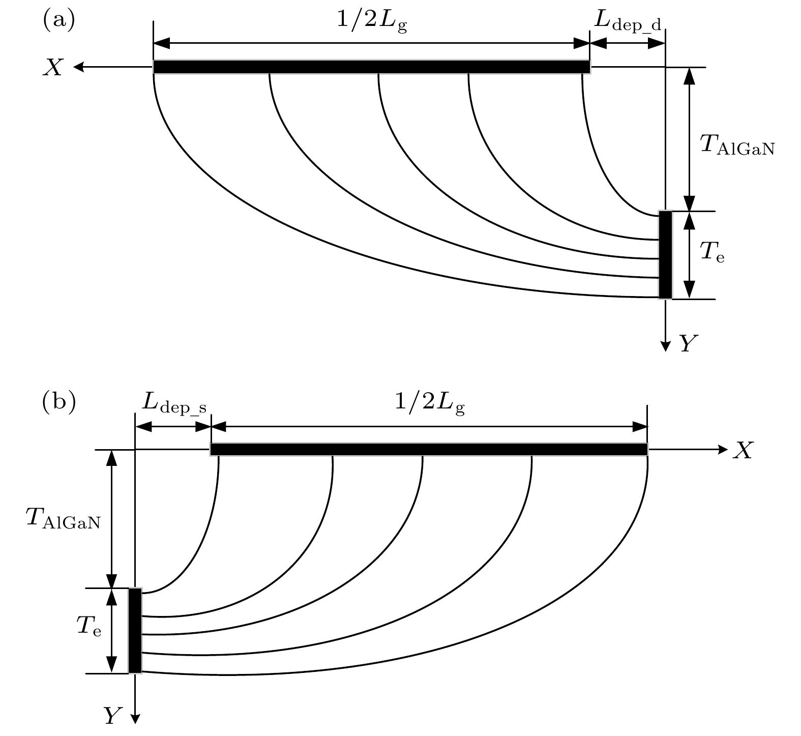
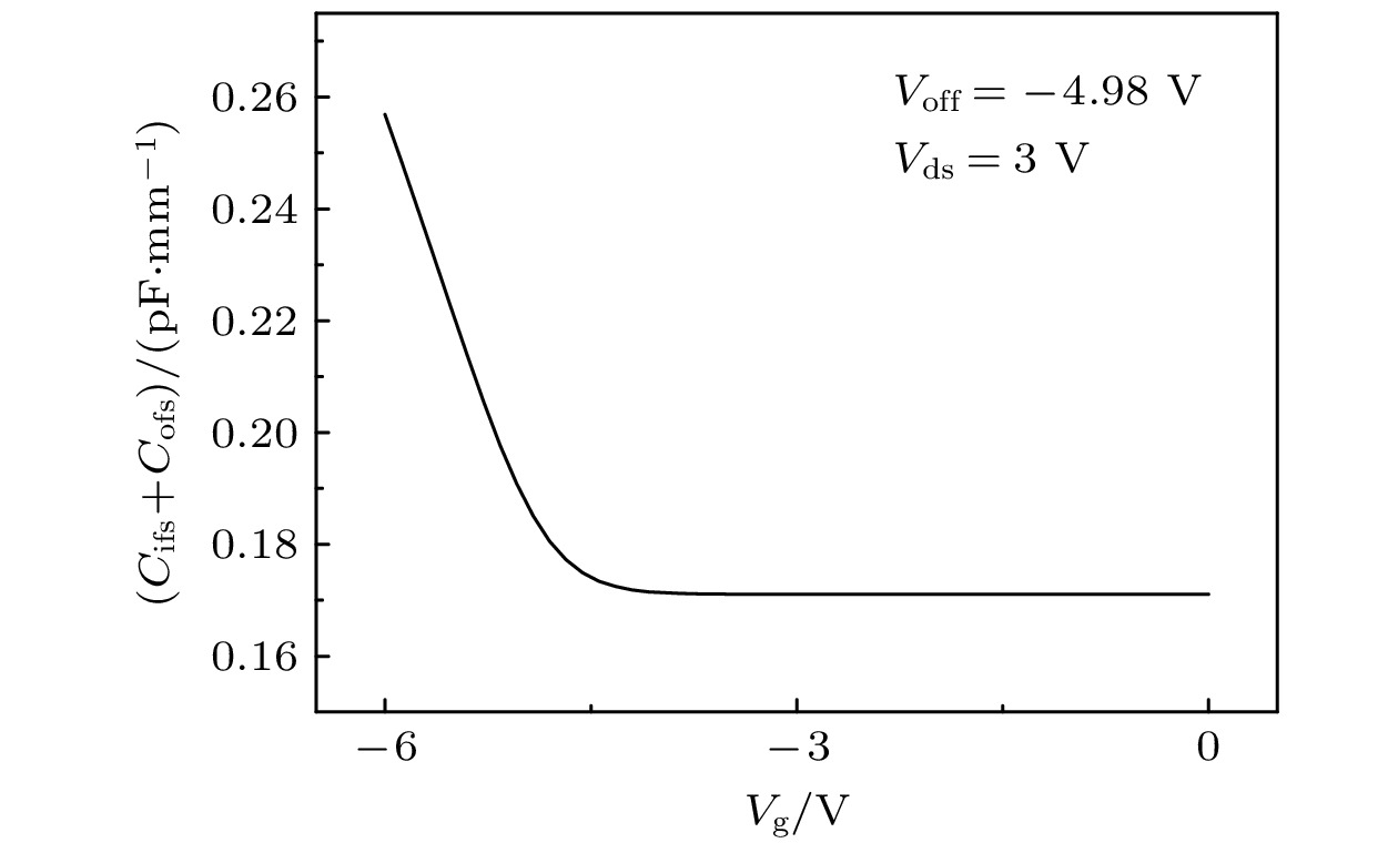
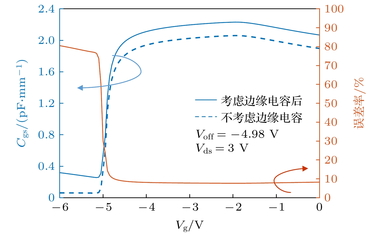
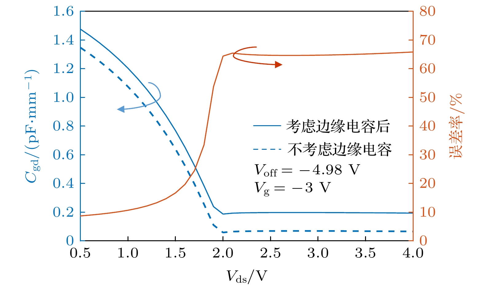
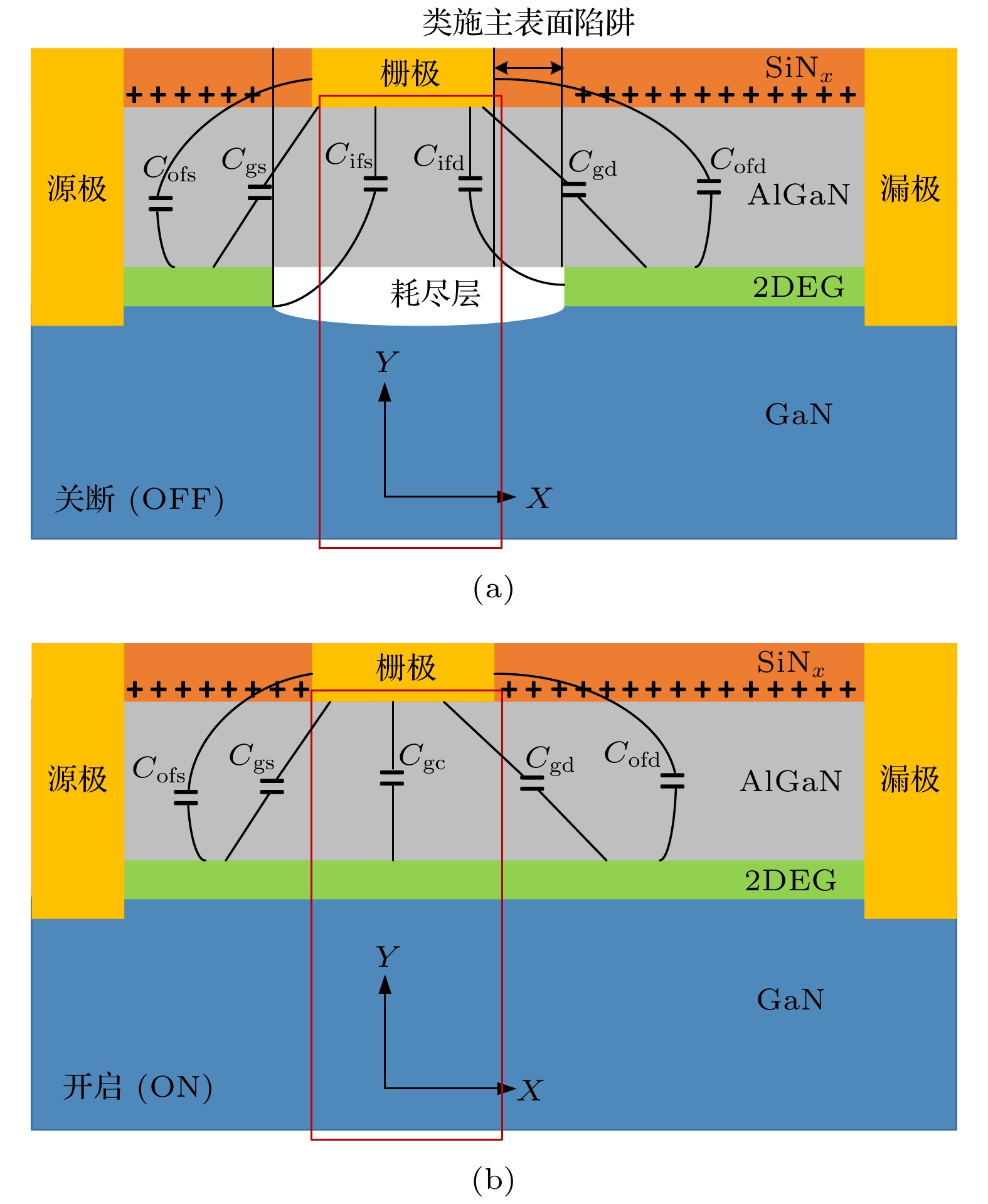
AlGaN/GaN 高电子迁移率晶体管的栅极电容由本征电容和边缘电容组成. 边缘电容分为外部边缘电容和内部边缘电容, 内部边缘电容相比外部边缘电容对器件的开关转换特性更为敏感. 本文基于内部边缘电容的形成机理, 推导了内部边缘电容Cifs/d模型, 进一步的分析表明, 其与器件的栅极偏置强相关; 基于Ward-Dutton电荷分配原则推导了相应的本征电容模型, 最后结合外部边缘电容得到了完整的栅极电容模型. 由于边缘电容是由器件结构产生的寄生电容, 仿真结果表明, 若不考虑边缘电容的影响, 栅源电容的误差可达80%以上, 而栅漏电容的误差可达65%以上. 因此, 在高频开关应用领域, 边缘电容对栅极电容的影响不可忽略.
The research on capacitance model of AlGaN/GaN high electron mobility transistor (HEMT) is of great significance in modern communication technology and circuit simulation. At present, many modeling methods of AlGaN/GaN HEMT capacitance models have been proposed. The gate capacitance is composed of intrinsic capacitance and fringe capacitance. However, most researches focus on the intrinsic capacitance but ignore the fringe capacitance, which leads to a large error in the final results. A total gate capacitance model including fringe capacitance needs to be established. In this paper, the conformal mapping method and transition functions are used to establish the inner fringe capacitance model, and the intrinsic capacitance model is derived based on the Ward-Dutton charge distribution principle. The intrinsic capacitance model and the outer fringe capacitance model are combined to obtain the source/drain total gate capacitance model. Based on this model, the relationship between the bias condition and the fringe capacitance is analyzed. We compare the difference between the effects of external bias on gate capacitance with and without the fringe capacitance considered, and the error rate of the gate capacitance in the on state is calculated without considering the fringe capacitance. The results show that the fringe capacitance is mainly affected by the gate bias. When the fringe capacitance is taken into account in the intrinsic capacitance model, the total capacitance model is larger than that without considering the fringe capacitance. For the gate capacitance, if the influence of fringing capacitance is not considered, the gate capacitance error rate of the device in the OFF state can reach 80%; for fringing capacitance, the error rate is over 65% when the device is working in the saturation region. -
Keywords:
- high electron mobility transistor /
- inner fringing capacitance /
- total gate capacitance /
- model
[1] Chow Paul T 2014 Materials Science Forum 778–780 1077
[2] [3] Chowdhury S, Stum Z, Li Z, Ueno K, Chow T P 2014 Materials Science Forum 778–780 971
 Google Scholar
[4] Millan J, Godignon P, Perpina X, Perez-Tomas A, Rebollo J 2014 IEEE Trans. Power Electron. 29 2155
 Google Scholar
[5] Tolbert L M 2008 Ph. D. Dissertation (Tennessee: Oak Ridge National Laboratory)
[6] Bindra A 2015 IEEE Power Electron. Mag. 2 42
 Google Scholar
[7] Jones E A, Fei F W, Costinett D 2016 IEEE J. Emerging Sel. Top. Power Electron. 4 707
 Google Scholar
[8] Ward D, Dutton R W 1978 IEEE Trans. Electron Devices 13 703
 Google Scholar
[9] Yigletu F M, Khandelwal S, Fjeldly T A, Iniguez B 2013 IEEE Trans. Electron Devices 60 3746
 Google Scholar
[10] Li K, Rakheja S 2018 Device Research Conference-Conference Digest Santa Barbara, California, USA, June 24–27, 2018 p1
[11] Jia Y H, Xu Y, Wen Z, Wu Y, Guo Y 2019 IEEE Trans. Electron Devices 66 357
 Google Scholar
[12] Bansal A, Paul B C, Roy K 2005 IEEE Trans. Electron Devices 52 256
 Google Scholar
[13] Koudymov A, Shur M S, Simin G 2007 IEEE Electron Device Lett. 28 332
 Google Scholar
[14] Tirado J M, Sanchez R J L, Izpura J I 2007 IEEE Trans. Electron Devices 54 410
 Google Scholar
[15] Simin G, Koudymov A, Tarakji A, Hu X, Yang J, Khan M A, Shur M S, Gaska R 2001 Appl. Phys. Lett. 79 2651
 Google Scholar
[16] Cheng X, Li M, Wang Y 2009 IEEE Trans. Electron Devices 56 12
 Google Scholar
[17] Yigletu F M, Iniguez B, Khandelwal S, Fjeldly T A 2013 International Conference on Simulation of Semiconductor Processes and Devices (SISPAD) Glasgow, UK, September 3–5, 2013 p13879917
[18] Khandelwal S, Yigletu F M, Iniguez B, Fjeldly T A 2013 Solid-state Electron. 82 38
 Google Scholar
[19] Swamy N S, Dutta A K 2018 IEEE Trans. Electron Devices 65 936
 Google Scholar
[20] 刘乃漳, 张雪冰, 姚若河 2020 69 077302
 Google Scholar
Liu N Z, Zhang X B, Yao R H 2020 Acta Phys. Sin. 69 077302
 Google Scholar
[21] Jia Y, Xu Y, Kai L, Zhang W, Huang A D, Guo Y X 2018 IEEE Trans. Electron Devices 65 3169
 Google Scholar
-
表 1 器件模型的参数值
Table 1. Parameter of the device model.
参数 定义 数值 Ls/μm 源端沟道长度 0.15 εx 有效介电常数 7.65ε0 Esat/(V⋅μm–1) 饱和电场 15 Ld/μm 漏端沟道长度 1 Ldep_s/nm 漏断耗尽层长度 12 Ldep_d/nm 漏端沟道长度 22 TAlGaN/nm AlGaN势垒层厚度 22 Te/nm 二维电子气厚度 8 Lg/μm 栅极长度 0.35 ζ 拟合参数 0.4 ζ2 拟合参数 0.3 δ1 拟合参数 –10.35 δ2 拟合参数 13.6 β2 拟合参数 20 -
[1] Chow Paul T 2014 Materials Science Forum 778–780 1077
[2] [3] Chowdhury S, Stum Z, Li Z, Ueno K, Chow T P 2014 Materials Science Forum 778–780 971
 Google Scholar
[4] Millan J, Godignon P, Perpina X, Perez-Tomas A, Rebollo J 2014 IEEE Trans. Power Electron. 29 2155
 Google Scholar
[5] Tolbert L M 2008 Ph. D. Dissertation (Tennessee: Oak Ridge National Laboratory)
[6] Bindra A 2015 IEEE Power Electron. Mag. 2 42
 Google Scholar
[7] Jones E A, Fei F W, Costinett D 2016 IEEE J. Emerging Sel. Top. Power Electron. 4 707
 Google Scholar
[8] Ward D, Dutton R W 1978 IEEE Trans. Electron Devices 13 703
 Google Scholar
[9] Yigletu F M, Khandelwal S, Fjeldly T A, Iniguez B 2013 IEEE Trans. Electron Devices 60 3746
 Google Scholar
[10] Li K, Rakheja S 2018 Device Research Conference-Conference Digest Santa Barbara, California, USA, June 24–27, 2018 p1
[11] Jia Y H, Xu Y, Wen Z, Wu Y, Guo Y 2019 IEEE Trans. Electron Devices 66 357
 Google Scholar
[12] Bansal A, Paul B C, Roy K 2005 IEEE Trans. Electron Devices 52 256
 Google Scholar
[13] Koudymov A, Shur M S, Simin G 2007 IEEE Electron Device Lett. 28 332
 Google Scholar
[14] Tirado J M, Sanchez R J L, Izpura J I 2007 IEEE Trans. Electron Devices 54 410
 Google Scholar
[15] Simin G, Koudymov A, Tarakji A, Hu X, Yang J, Khan M A, Shur M S, Gaska R 2001 Appl. Phys. Lett. 79 2651
 Google Scholar
[16] Cheng X, Li M, Wang Y 2009 IEEE Trans. Electron Devices 56 12
 Google Scholar
[17] Yigletu F M, Iniguez B, Khandelwal S, Fjeldly T A 2013 International Conference on Simulation of Semiconductor Processes and Devices (SISPAD) Glasgow, UK, September 3–5, 2013 p13879917
[18] Khandelwal S, Yigletu F M, Iniguez B, Fjeldly T A 2013 Solid-state Electron. 82 38
 Google Scholar
[19] Swamy N S, Dutta A K 2018 IEEE Trans. Electron Devices 65 936
 Google Scholar
[20] 刘乃漳, 张雪冰, 姚若河 2020 69 077302
 Google Scholar
Liu N Z, Zhang X B, Yao R H 2020 Acta Phys. Sin. 69 077302
 Google Scholar
[21] Jia Y, Xu Y, Kai L, Zhang W, Huang A D, Guo Y X 2018 IEEE Trans. Electron Devices 65 3169
 Google Scholar
计量
- 文章访问数: 10660
- PDF下载量: 265
- 被引次数: 0


 下载:
下载:

