


-
作为最重要的第三代半导体材料之一, 纳米氮化镓(GaN)也引起了人们的广泛关注与重视. 本文采用微波等离子体化学气相沉积(microwave plasma chemical vapor deposition, MPCVD)系统, 成功地制备出了四方截面的GaN纳米线, 其纳米线半径为300—500 nm, 长度为15—20 μm. 研究发现, 通过调控掺杂Mg的比例, 可以实现其截面结构从三方向四方转变. 通过进一步地研究Mg掺杂调控其截面结构的物理机制, 提出其三方-四方截面结构的转变应该来源于其纳米线的气-液-固(VLS)生长向自催化气-固(VS)生长模式的转变. 对所制备的纳米线进行了光致发光(photoluminescence, PL)光谱分析, 结果表明四方结构Mg掺杂GaN纳米线发光峰红移至386 nm. 采用所制备的纳米线进行了场发射性能研究, 结果表明四方结构Mg掺杂GaN纳米线开启电场为5.2 V/μm, 并能保持较高电流密度, 相较于三方结构未掺杂GaN纳米线场发射性能有一定提高, 进而分析掺杂以及形貌结构对GaN纳米线场发射的影响机制. 研究结果不仅给出了一种四方结构GaN纳米线的制备方法, 同时也为纳米线结构调控提出了新的思路与方法, 将为新型纳米线器件设计与制作提供了新的技术手段.GaN nanomaterials, as one of the most important third-generation semiconductor materials, have attracted wide attention. In this study, GaN nanowires with square cross section were successfully prepared by microwave plasma chemical vapor deposition system. The diameters of nanowires are from 300 to 500 nm and the lengths from 15 to 20 μm. The results show that the cross section of nanowires could be transformed from triangle into square by adjusting the ratio of Mg to Ga in source materials. X-ray diffraction(XRD)result indicate that the structure of GaN nanowires are agree with the hexagonal wurtzite. X-ray photoelectron spectroscopy (XPS) rusult show that a certain amount of Mg and O impurities incoporated in the square-shaped GaN nanowires. Transmission electron microscopy (TEM) result suggested that square-shaped GaN nanowires had high crystallinity with a growth direction of [
$0\bar 110$ ]. The ratio of source materials- and time-depented growth mechanism was also studied. It was suggested that the transformation of the cross section from triangle to square structure should be derived from the growth mechanism change from vapor-liquid-solid(VLS)process to vapor-solid(VS)process. The doped Mg increased the growth rate of the nanowires sidewalls, which led to a symmetrically growth of GaN nanowires along the twin boundaries. GaN nanowires gradually transformed to square structure by auto-catalytic growth. Moreover, the property of field emission were further investigated. The results showed that the turn-on electric field of square-shaped GaN nanowires was 5.2 V/m and a stable field emission property at high electric field. This research provides a new method for the preparation of square-shaped GaN nanowires and a prospective way for the design and fabrication of novel nano-scale devices.-
Keywords:
- gallium nitride(GaN) /
- square-shaped nanowires /
- Mg doped /
- field emission
[1] Han S, Choi I, Lee C R, Jeong K U, Lee S K, Kim J S 2020 ACS Appl. Mater. Inter. 12 970
 Google Scholar
[2] Guo D X, Wang X F, Wang H, Song W D, Chen H, Qi M Y, Luo X J, Luo X, Li G, Qin G G, Li S T 2018 ACS Photonics 5 4810
Google Scholar
[3] Ko S M, Hur J, Lee C, Isnaeni, Gong S H, Kim M, Cho Y H 2020 Sci. Rep. 10 358
Google Scholar
[4] 邓长发, 燕少安, 王冬, 彭金峰, 郑学军 2019 68 237304
Google Scholar
Deng C F, Yan S A, Wang D, Peng J F, Zheng X J 2019 Acta Phys. Sin. 68 237304
Google Scholar
[5] Liu B, Hu T, Wang Z, Liu L, Qin F, Huang N, Jiang X 2012 Cryst. Res. Technol. 47 207
Google Scholar
[6] Sahoo P, Dhara S, Amirthapandian S, Kamruddin M 2013 J Mater. Chem. C 1 7237
Google Scholar
[7] Johar M A, Song H G, Waseem A, Hassan M A, Bagal I V, Cho Y H, Ryu S W 2020 Appl. Mater. Today 19 100541
Google Scholar
[8] Liao H, Wei T T, Zong H, Jiang S X, Li J C, Yang Y, Yu G, Wen P J, Lang R, Wang W J, Hu X D 2019 Appl. Surf. Sci. 489 346
Google Scholar
[9] Morassi M, Guan N, Dubrovskii V G, Berdnikov Y, Barbier C, Mancini L, Largeau L, Babichev A V, Kumaresan V, Julien F H, Travers L, Gogneau N, Harmand J C, Tchernycheva M 2019 Cryst. Growth Des. 20 552
[10] Treeck D v, Garrido S F, Geelhaar L 2020 Phys. Rev. Mater. 4 013404
Google Scholar
[11] Sun J M, Han M M, Gu Y, Yang Z X, Zeng H B 2018 Adv. Optical Mater. 6 1800256
Google Scholar
[12] 赵军伟, 张跃飞, 宋雪梅, 严辉, 王如志 2014 63 117702
Google Scholar
Zhao J W, Zhang Y F, Song X M, Yan H, Wang R Z 2014 Acta Phys. Sin. 63 117702
Google Scholar
[13] Ji Y H, Wang R Z, Feng X Y, Zhang Y F, Yan H 2017 J. Phys. Chem. C 121 24804
Google Scholar
[14] Feng X Y, Wang R Z, Liang Q, Ji Y H, Yang M Q 2019 Cryst. Growth Des. 19 2687
Google Scholar
[15] Zhao J W, Zhang Y F, Li Y H, Su C H, Song X M, Yan H, Wang R Z 2015 Sci. Rep. 5 17692
Google Scholar
[16] Bernal R A, Agrawal R, Peng B, Bertness K A, Sanford N A 2011 Nano Lett. 11 548
Google Scholar
[17] Pozina G, Gubaydullin A R, Mitrofanov M I, Kaliteevski M A, Levitskii I V, Voznyuk G V, Tatarinov E E 2018 Sci. Rep. 8 7218
Google Scholar
[18] Ross F M, Tersoff J, Reuter M C 2005 Phys. Rev. Lett. 95 146104
Google Scholar
[19] Gholampour M, Abdollah-zadeh A, Poursalehi R, Shekari L 2014 Mater. Lett. 120 136
Google Scholar
[20] Srivastava P, Kumar A, Jaiswal N K, Sharma V 2016 Proceeding of International Conference on Condensed Matter and Applied Physics Bikaner, INDIA, OCT 30–31, 2015 p020071
[21] Srivastava P, Kumar A, Jaiswal N K, Sharma V 2016 Phys. Status Solidi B 253 2185
Google Scholar
[22] Wang Y Q, Wang R Z, Zhu M K, Wang B B, Yan H 2013 Appl. Surf. Sci. 285 115
Google Scholar
[23] Liu B D, Bando Y, Tang C C, Xu F F 2005 J. Phys. Chem. B 109 21521
Google Scholar
[24] Li E L, Wu B, Lv S T, Cui Z, Ma D M, Shi W 2016 J. Alloy. Compd. 681 324
Google Scholar
[25] Xia S H, Liu L, Diao Y, Feng S 2017 J. Appl. Phys. 122 135102
Google Scholar
[26] Pan C J, Chi G C 1999 Solid State Electron. 43 621
Google Scholar
[27] Jaud A, Auvray L, Kahouli A, Abi-Tannous T, Cauwet F, Ferro G, Brylinski C 2017 Phys. Status Solidi A 214 1600428
Google Scholar
[28] Bae S Y, Lekhal K, Lee H J, Min J W, Lee D S, Honda Y, Amano H 2017 Phy. Status Solidi B 254 1600722
Google Scholar
[29] Kamimura J, Bogdanoff P, Ramsteiner M, Corfdir P, Feix F, Geelhaar L, Riechert H 2017 Nano Lett. 17 1529
Google Scholar
[30] Siladie A M, Amichi L, Mollard N, Mouton I, Bonef B, Bougerol C, Grenier A, Robin E, Jouneau P H, Garro N, Cros A, Daudin B 2018 Nanotechnology 29 255706
Google Scholar
[31] Miceli G, Pasquarello A 2016 Phys.l Rev. B 93 165207
Google Scholar
[32] Wang Y Q, Wang R Z, Li Y J, Zhang Y F, Zhu M K, Wang B B, Yan H 2013 CrystEngComm 15 1626
Google Scholar
[33] Lymperakis L, Neugebauer J 2009 Phys. Rev. B 79 241308
Google Scholar
[34] Limbach F, Caterino R, Gotschke T, Stoica T, Calarco R, Geelhaar L, Riechert H 2012 AIP Advances 2 012157
Google Scholar
[35] Nayak S, Kumar R, Pandey N, Nagaraja K K, Gupta M, Shivaprasad S M 2018 J. Appl. Phys. 123 135303
Google Scholar
[36] Park J B, Kim N J, Kim Y J, Lee S H, Yi G C 2014 Curr. Appl. Phys. 14 1437
Google Scholar
[37] Ji Y H, Wang R Z, Yang M Q, Feng X Y, Zhang Y F, Huang A P, Yang L X, Liu Y Q, Yan Y Z, Yan H 2020 J. Phys. Chem. C 124 6725
Google Scholar
[38] Li Z J, Li W D, Wang X L, Zhang M 2014 Phys. Status Solidi A 211 1550
Google Scholar
[39] Consonni V, Knelangen M, Geelhaar L, Trampert A, Riechert H 2010 Phys. Rev. B 81 085310
Google Scholar
[40] Zhang D D, Xue C S, Zhuang H Z, Sun H B, Cao Y P, Huang Y L, Wang Z P, Wang Y 2009 Chemphyschem 10 571
Google Scholar
[41] Shi F, Huang Y L, Xue C S 2011 J. Exp. Nanosci. 6 174
Google Scholar
[42] Rackauskas S, Jiang H, Wagner J B, Shandakov S D, Hansen T W, Kauppinen E I, Nasibulin A G 2014 Nano Lett. 14 5810
Google Scholar
[43] Gamalski A D, Voorhees P W, Ducati C, Sharma R, Hofmann S 2014 Nano Lett. 14 1288
Google Scholar
[44] Boukhicha R, Gardès C, Vincent L, Renard C, Yam V, Fossard F, Patriarche G, Jabeen F, Bouchier D 2011 EPL 95 18004
Google Scholar
[45] Ngo T H, Gil B, Shubina T V, Damilano B, Vezian S, Valvin P, Massies J 2018 Sci. Rep. 8 15767
Google Scholar
[46] Reshchikov M A, Morkoç H 2005 J. Appl. Phys. 97 061301
Google Scholar
[47] Kaufmann U, Kunzer M, Maier M, Obloh H, Ramakrishnan A, Santic B, Schlotter P 1998 Appl. Phys. Lett. 72 1326
Google Scholar
[48] Stoica T, Calarco R 2011 IEEE J. Sel. Top. Quant. 17 859
Google Scholar
[49] Das S N, Patra S, Kar J P, Lee M J, Hwang S H, Lee T I, Myoung J M 2013 Mater. Lett. 106 352
Google Scholar
[50] Bayel M W, Brandt M S, Glaser E R, Wickenden A E, D. K D, Henry R L, Stutzmann M 1999 Phys. Ptat. Pol. B 216 547
[51] Glaser E R, Carlos W E, Braga G C B 2002 Phys. Rev. B 65 085312
Google Scholar
[52] Wang R Z, Zhao W, Yan H 2017 Sci. Rep. 7 43625
Google Scholar
[53] Li W D, Zhang M, Li Y, Liu G X, Li Z J 2019 CrystEngComm 21 3993
Google Scholar
[54] Zhao W, Wang R Z, Song Z W, Wang H, Yan H, Chu P K 2013 J. Physl. Chem. C 117 1518
Google Scholar
[55] Vayssieres L, Graetzel M 2004 Angew. Chem. Int. Ed. Engl. 43 3666
Google Scholar
[56] Diao Y, Liu L, Xia S H, Feng S, Lu F F 2018 Superlattice Microst. 115 140
Google Scholar
[57] Wang Z, Chen Y H, Ye X L 2004 13th International Conference on Semiconducting and Insulating Materials Beijing, China, Sep. 20–25, 2004 pp57–60
-

图 1 不同原料配比制备Mg掺杂GaN纳米线的FESEM图 (a)样品A-a; (b)样品A-b; (c)样品A-c; (d)样品A-d; (e)样品A-e
Fig. 1. FESEM images Mg doped GaN nanowires prepared at different source materials ratio. (a) Sample A-a; (b) sample A-b; (c) sample A-c; (d) sample A-d; (e) sample A-e.
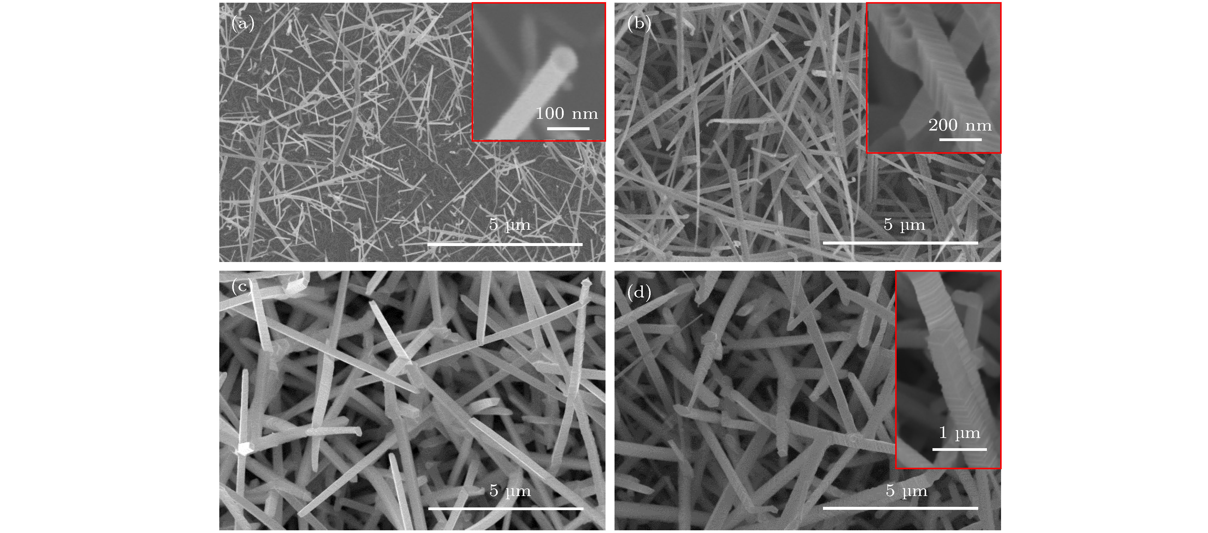
图 2 不同生长时间制备Mg掺杂GaN纳米线的FESEM图 (a)样品B-a; (b)样品B-b; (c)样品B-c; (d)样品B-d
Fig. 2. FESEM images Mg doped GaN nanowires prepared at different growth times. (a) Sample B-a; (b) sample B-b; (c) sample B-c; (d) sample B-d.

图 5 样品A-e的(a) TEM图; (b) HRTEM图插图为样品A-e的SAED图
Fig. 5. (a) TEM image; (b) HRTEM image and SAED pattern (inset) of sample A-e.
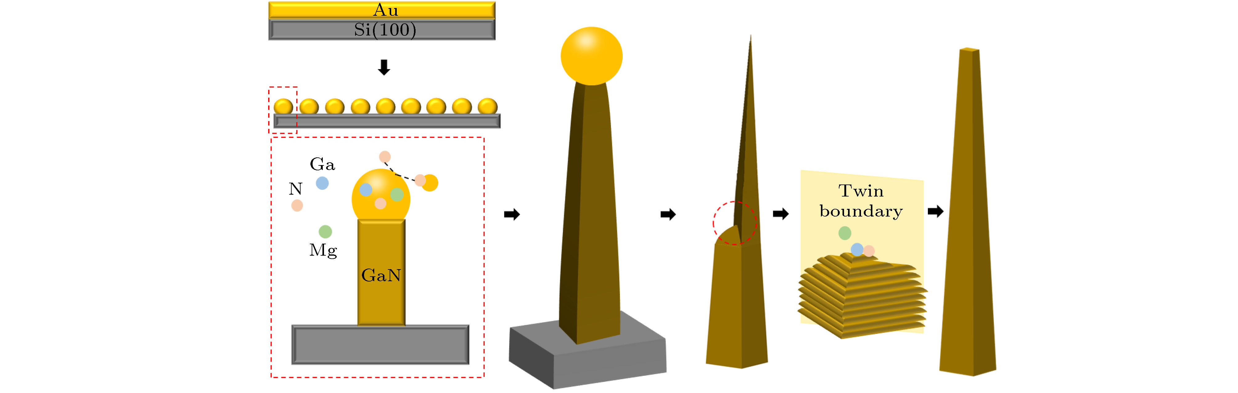
图 6 四方结构GaN纳米线的成核和生长过程示意图
Fig. 6. Schematic diagram of nucleation and growth for square-shaped GaN nanowires.

图 7 (a)样品A-a及样品A-e的PL图谱;(b)样品A-e的带隙分析图
Fig. 7. (a) PL spectra of sample A-a and sample A-e; (b) band gap analysis spectra of sample A-e.
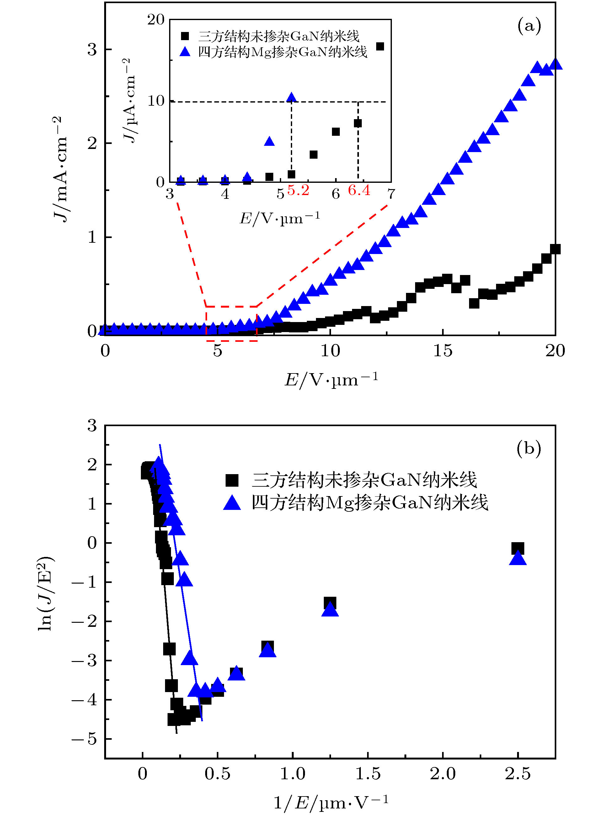
图 8 样品A-a及样品A-e的(a) J-E曲线; (b) F-N曲线
Fig. 8. (a) J-E curves; (b) F-N curves of sample A-a and sample A-e.
表 1 不同原料配比制备Mg掺杂GaN纳米线的实验参数
Table 1. The experimental parameter of preparing Mg doped GaN nanowiresat different source materials ratio.
编号 N2/sccm 气压/Torr T/℃ t/min 微波功率/W C∶Ga2O3∶MgO A-a 13 10 870 30 300 12∶1∶0 A-b 13 10 870 30 300 12:1:0.2 A-c 13 10 870 30 300 12∶1∶0.5 A-d 13 10 870 30 300 12∶1∶1 A-e 13 10 870 30 300 12∶1∶1.5  下载: 导出CSV
表 2 不同生长时间制备Mg掺杂GaN纳米线的实验参数
Table 2. The experimental parameter of preparing Mg doped GaN nanowiresat different growth time.
编号 N2/sccm 气压/Torr T/℃ t/min 微波功率/W C∶Ga2O3∶MgO B-a 13 10 870 10 300 12∶1∶1.5 B-b 13 10 870 20 300 12∶1∶1.5 B-c 13 10 870 30 300 12∶1∶1.5 B-d 13 10 870 40 300 12∶1∶1.5
下载: 导出CSV
-
[1] Han S, Choi I, Lee C R, Jeong K U, Lee S K, Kim J S 2020 ACS Appl. Mater. Inter. 12 970
Google Scholar
[2] Guo D X, Wang X F, Wang H, Song W D, Chen H, Qi M Y, Luo X J, Luo X, Li G, Qin G G, Li S T 2018 ACS Photonics 5 4810
Google Scholar
[3] Ko S M, Hur J, Lee C, Isnaeni, Gong S H, Kim M, Cho Y H 2020 Sci. Rep. 10 358
Google Scholar
[4] 邓长发, 燕少安, 王冬, 彭金峰, 郑学军 2019 68 237304
Google Scholar
Deng C F, Yan S A, Wang D, Peng J F, Zheng X J 2019 Acta Phys. Sin. 68 237304
Google Scholar
[5] Liu B, Hu T, Wang Z, Liu L, Qin F, Huang N, Jiang X 2012 Cryst. Res. Technol. 47 207
Google Scholar
[6] Sahoo P, Dhara S, Amirthapandian S, Kamruddin M 2013 J Mater. Chem. C 1 7237
Google Scholar
[7] Johar M A, Song H G, Waseem A, Hassan M A, Bagal I V, Cho Y H, Ryu S W 2020 Appl. Mater. Today 19 100541
Google Scholar
[8] Liao H, Wei T T, Zong H, Jiang S X, Li J C, Yang Y, Yu G, Wen P J, Lang R, Wang W J, Hu X D 2019 Appl. Surf. Sci. 489 346
Google Scholar
[9] Morassi M, Guan N, Dubrovskii V G, Berdnikov Y, Barbier C, Mancini L, Largeau L, Babichev A V, Kumaresan V, Julien F H, Travers L, Gogneau N, Harmand J C, Tchernycheva M 2019 Cryst. Growth Des. 20 552
[10] Treeck D v, Garrido S F, Geelhaar L 2020 Phys. Rev. Mater. 4 013404
Google Scholar
[11] Sun J M, Han M M, Gu Y, Yang Z X, Zeng H B 2018 Adv. Optical Mater. 6 1800256
Google Scholar
[12] 赵军伟, 张跃飞, 宋雪梅, 严辉, 王如志 2014 63 117702
Google Scholar
Zhao J W, Zhang Y F, Song X M, Yan H, Wang R Z 2014 Acta Phys. Sin. 63 117702
Google Scholar
[13] Ji Y H, Wang R Z, Feng X Y, Zhang Y F, Yan H 2017 J. Phys. Chem. C 121 24804
Google Scholar
[14] Feng X Y, Wang R Z, Liang Q, Ji Y H, Yang M Q 2019 Cryst. Growth Des. 19 2687
Google Scholar
[15] Zhao J W, Zhang Y F, Li Y H, Su C H, Song X M, Yan H, Wang R Z 2015 Sci. Rep. 5 17692
Google Scholar
[16] Bernal R A, Agrawal R, Peng B, Bertness K A, Sanford N A 2011 Nano Lett. 11 548
Google Scholar
[17] Pozina G, Gubaydullin A R, Mitrofanov M I, Kaliteevski M A, Levitskii I V, Voznyuk G V, Tatarinov E E 2018 Sci. Rep. 8 7218
Google Scholar
[18] Ross F M, Tersoff J, Reuter M C 2005 Phys. Rev. Lett. 95 146104
Google Scholar
[19] Gholampour M, Abdollah-zadeh A, Poursalehi R, Shekari L 2014 Mater. Lett. 120 136
Google Scholar
[20] Srivastava P, Kumar A, Jaiswal N K, Sharma V 2016 Proceeding of International Conference on Condensed Matter and Applied Physics Bikaner, INDIA, OCT 30–31, 2015 p020071
[21] Srivastava P, Kumar A, Jaiswal N K, Sharma V 2016 Phys. Status Solidi B 253 2185
Google Scholar
[22] Wang Y Q, Wang R Z, Zhu M K, Wang B B, Yan H 2013 Appl. Surf. Sci. 285 115
Google Scholar
[23] Liu B D, Bando Y, Tang C C, Xu F F 2005 J. Phys. Chem. B 109 21521
Google Scholar
[24] Li E L, Wu B, Lv S T, Cui Z, Ma D M, Shi W 2016 J. Alloy. Compd. 681 324
Google Scholar
[25] Xia S H, Liu L, Diao Y, Feng S 2017 J. Appl. Phys. 122 135102
Google Scholar
[26] Pan C J, Chi G C 1999 Solid State Electron. 43 621
Google Scholar
[27] Jaud A, Auvray L, Kahouli A, Abi-Tannous T, Cauwet F, Ferro G, Brylinski C 2017 Phys. Status Solidi A 214 1600428
Google Scholar
[28] Bae S Y, Lekhal K, Lee H J, Min J W, Lee D S, Honda Y, Amano H 2017 Phy. Status Solidi B 254 1600722
Google Scholar
[29] Kamimura J, Bogdanoff P, Ramsteiner M, Corfdir P, Feix F, Geelhaar L, Riechert H 2017 Nano Lett. 17 1529
Google Scholar
[30] Siladie A M, Amichi L, Mollard N, Mouton I, Bonef B, Bougerol C, Grenier A, Robin E, Jouneau P H, Garro N, Cros A, Daudin B 2018 Nanotechnology 29 255706
Google Scholar
[31] Miceli G, Pasquarello A 2016 Phys.l Rev. B 93 165207
Google Scholar
[32] Wang Y Q, Wang R Z, Li Y J, Zhang Y F, Zhu M K, Wang B B, Yan H 2013 CrystEngComm 15 1626
Google Scholar
[33] Lymperakis L, Neugebauer J 2009 Phys. Rev. B 79 241308
Google Scholar
[34] Limbach F, Caterino R, Gotschke T, Stoica T, Calarco R, Geelhaar L, Riechert H 2012 AIP Advances 2 012157
Google Scholar
[35] Nayak S, Kumar R, Pandey N, Nagaraja K K, Gupta M, Shivaprasad S M 2018 J. Appl. Phys. 123 135303
Google Scholar
[36] Park J B, Kim N J, Kim Y J, Lee S H, Yi G C 2014 Curr. Appl. Phys. 14 1437
Google Scholar
[37] Ji Y H, Wang R Z, Yang M Q, Feng X Y, Zhang Y F, Huang A P, Yang L X, Liu Y Q, Yan Y Z, Yan H 2020 J. Phys. Chem. C 124 6725
Google Scholar
[38] Li Z J, Li W D, Wang X L, Zhang M 2014 Phys. Status Solidi A 211 1550
Google Scholar
[39] Consonni V, Knelangen M, Geelhaar L, Trampert A, Riechert H 2010 Phys. Rev. B 81 085310
Google Scholar
[40] Zhang D D, Xue C S, Zhuang H Z, Sun H B, Cao Y P, Huang Y L, Wang Z P, Wang Y 2009 Chemphyschem 10 571
Google Scholar
[41] Shi F, Huang Y L, Xue C S 2011 J. Exp. Nanosci. 6 174
Google Scholar
[42] Rackauskas S, Jiang H, Wagner J B, Shandakov S D, Hansen T W, Kauppinen E I, Nasibulin A G 2014 Nano Lett. 14 5810
Google Scholar
[43] Gamalski A D, Voorhees P W, Ducati C, Sharma R, Hofmann S 2014 Nano Lett. 14 1288
Google Scholar
[44] Boukhicha R, Gardès C, Vincent L, Renard C, Yam V, Fossard F, Patriarche G, Jabeen F, Bouchier D 2011 EPL 95 18004
Google Scholar
[45] Ngo T H, Gil B, Shubina T V, Damilano B, Vezian S, Valvin P, Massies J 2018 Sci. Rep. 8 15767
Google Scholar
[46] Reshchikov M A, Morkoç H 2005 J. Appl. Phys. 97 061301
Google Scholar
[47] Kaufmann U, Kunzer M, Maier M, Obloh H, Ramakrishnan A, Santic B, Schlotter P 1998 Appl. Phys. Lett. 72 1326
Google Scholar
[48] Stoica T, Calarco R 2011 IEEE J. Sel. Top. Quant. 17 859
Google Scholar
[49] Das S N, Patra S, Kar J P, Lee M J, Hwang S H, Lee T I, Myoung J M 2013 Mater. Lett. 106 352
Google Scholar
[50] Bayel M W, Brandt M S, Glaser E R, Wickenden A E, D. K D, Henry R L, Stutzmann M 1999 Phys. Ptat. Pol. B 216 547
[51] Glaser E R, Carlos W E, Braga G C B 2002 Phys. Rev. B 65 085312
Google Scholar
[52] Wang R Z, Zhao W, Yan H 2017 Sci. Rep. 7 43625
Google Scholar
[53] Li W D, Zhang M, Li Y, Liu G X, Li Z J 2019 CrystEngComm 21 3993
Google Scholar
[54] Zhao W, Wang R Z, Song Z W, Wang H, Yan H, Chu P K 2013 J. Physl. Chem. C 117 1518
Google Scholar
[55] Vayssieres L, Graetzel M 2004 Angew. Chem. Int. Ed. Engl. 43 3666
Google Scholar
[56] Diao Y, Liu L, Xia S H, Feng S, Lu F F 2018 Superlattice Microst. 115 140
Google Scholar
[57] Wang Z, Chen Y H, Ye X L 2004 13th International Conference on Semiconducting and Insulating Materials Beijing, China, Sep. 20–25, 2004 pp57–60


 下载:
下载:


计量
- 文章访问数: 11100
- PDF下载量: 161
- 被引次数: 0
