


-
半导体加工工艺微缩过程中, 硅基材料的短沟道效应带来的低能效促使研究人员寻找新型半导体替代材料. 二维半导体因其原子级别的厚度以及范德瓦耳斯表面而倍受关注, 二维硒氧化铋就是其中迁移率、稳定性以及成本各方面较为均衡的一种. 然而, 其制备受到基底很严格的限制, 导致器件加工难度较大. 本文利用化学气相沉积法直接在硅片基底上合成出规格为25 µm×51.0 nm(厚度)的二维硒氧化铋, 并通过拉曼光谱、原子力显微镜、扫描电子显微镜、X射线能谱对其进行表征. 同时, 通过场效应晶体管输运的测试得出其迁移率为80.0 cm2/(V·s)以及光电探测得出其具有2.45×104 A/W的光响应度和6×104的光增益等比较出色的表现. 但由于厚度较大, 导致其场效应管开关比低(2500)以及不高的光电探测灵敏度(5×10¹⁰ Jones). 由此可知, 硅片基底虽然带来器件加工上的便利性, 但有待进一步优化生长, 并集成更多种材料的应用.As the scaling-down of semiconductor processing technology goes on, it is urgent to find the successor of silicon-based materials since the severe short channel effect lowers down their energy efficiency as logic devices. Owing to its atomic thickness and van der Waals surface, two-dimensional semiconductors have received huge attention in this area, among which Bi2O2Se has achieved a good trade-off among the carrier mobility, stability and costing. However, the synthesis of Bi2O2Se need some polarized substrates, which hinders its processing and application. Here, a Bi2O2Se layer with 25 µm in size and 51.0 nm in thickness is directly synthesized on a silicon substrate via chemical vapor deposition . A Field-effect transistor with a carrier mobility of 80.0 cm2/(V·s) and phototransistor with a photoresponsivity of 2.45×10⁴ A/W and a photogain of 6×10⁴ is also demonstrated, which hpossesses quite outstanding photodetection performance. Nevertheless, the high dark current and low on/off ratio brought by the large thickness leads to a fair detectivity (5×10¹⁰ Jones). All in all, , although silicon substrate brings convenience in device fabricating, it is still needed to further optimizing the growth and integrating more applications of various two-dimensional materials .
-
Keywords:
- two-dimensional materials /
- chemical vapor deposition /
- Bi2O2Se /
- Photodetector
[1] 2021 IRDS Lithography Report
[2] Winstead B, Ravaioli U 2000 IEEE T. Electron Dev. 47 1241
 Google Scholar
[3] Hooper W, Lehrer W 1967 Proc. IEEE 55 1237
Google Scholar
[4] Sze S, Irvin J 1968 Solid-State Electron. 11 599
Google Scholar
[5] Asif Khan M, Kuznia J, Bhattarai A, Olson D 1993 Appl. Phys. Lett. 62 1786
Google Scholar
[6] Novoselov K S, Jiang D, Schedin F, Booth T J, Khotkevich V V, Morozov S V, Geim A K 2005 Proc. Natl. Acad. Sci. U S A 102 10451
Google Scholar
[7] Lee Y H, Zhang X Q, Zhang W, Chang M T, Lin C T, Chang K D, Yu Y C, Wang J T, Chang C S, Li L J, Lin T W 2012 Adv. Mater. 24 2320
Google Scholar
[8] Zhan Y, Liu Z, Najmaei S, Ajayan P M, Lou J 2012 Small 8 966
Google Scholar
[9] Duan X, Wang C, Shaw J C, Cheng R, Chen Y, Li H, Wu X, Tang Y, Zhang Q, Pan A 2014 Nat. Nanotechnol. 9 1024
Google Scholar
[10] Li L, Yu Y, Ye G J, Ge Q, Ou X, Wu H, Feng D, Chen X H, Zhang Y 2014 Nat. Nanotechnol. 9 372
Google Scholar
[11] Novoselov K S, Geim A K, Morozov S V, Jiang D, Zhang Y, Dubonos S V, Grigorieva I V, Firsov A A 2004 Science 306 666
Google Scholar
[12] Radisavljevic B, Radenovic A, Brivio J, Giacometti V, Kis A 2011 Nat. Nanotechnol. 6 147
Google Scholar
[13] Li W, Zhou J, Cai S, Yu Z, Zhang J, Fang N, Li T, Wu Y, Chen T, Xie X 2019 Nat. Electron. 2 563
Google Scholar
[14] Cronemeyer D C 1957 Phys. Rev. 105 522
Google Scholar
[15] Bandurin D A, Tyurnina A V, Geliang L Y, Mishchenko A, Zólyomi V, Morozov S V, Kumar R K, Gorbachev R V, Kudrynskyi Z R, Pezzini S 2017 Nat. Nanotechnol. 12 223
Google Scholar
[16] Chow W L, Yu P, Liu F, Hong J, Wang X, Zeng Q, Hsu C H, Zhu C, Zhou J, Wang X 2017 Adv. Mater. 29 1602969
Google Scholar
[17] Zhao Y, Qiao J, Yu Z, Yu P, Xu K, Lau S P, Zhou W, Liu Z, Wang X, Ji W 2017 Adv. Mater. 29 1604230
Google Scholar
[18] Wu J, Liu Y, Tan Z, Tan C, Yin J, Li T, Tu T, Peng H 2017 Adv. Mater. 29 1704060
Google Scholar
[19] Wu J, Tan C, Tan Z, Liu Y, Yin J, Dang W, Wang M, Peng H 2017 Nano Lett. 17 3021
Google Scholar
[20] Wu J, Yuan H, Meng M, Chen C, Sun Y, Chen Z, Dang W, Tan C, Liu Y, Yin J 2017 Nat. Nanotechnol. 12 530
Google Scholar
[21] Li T, Peng H 2021 Acc. Mater. Res. 2 842
Google Scholar
[22] Tan C, Tang M, Wu J, Liu Y, Li T, Liang Y, Deng B, Tan Z, Tu T, Zhang Y 2019 Nano Lett. 19 2148
Google Scholar
[23] Fu Q, Zhu C, Zhao X, Wang X, Chaturvedi A, Zhu C, Wang X, Zeng Q, Zhou J, Liu F 2019 Adv. Mater. 31 1804945
Google Scholar
[24] Seu K J, Pandey A P, Haque F, Proctor E A, Ribbe A E, Hovis J S 2007 Biophys. J. 92 2445
Google Scholar
[25] Liu Y, Guo J, Zhu E, Liao L, Lee S-J, Ding M, Shakir I, Gambin V, Huang Y, Duan X 2018 Nature 557 696
Google Scholar
[26] Grinvald A, Steinberg I Z 1974 Anal. Biochem. 59 583
Google Scholar
[27] Furchi M M, Polyushkin D K, Pospischil A, Mueller T 2014 Nano Lett. 14 6165
Google Scholar
[28] Gong X, Tong M, Xia Y, Cai W, Moon J S, Cao Y, Yu G, Shieh C-L, Nilsson B, Heeger A J 2009 Science 325 1665
Google Scholar
[29] Liu S, Wei Z, Cao Y, Gan L, Wang Z, Xu W, Guo X, Zhu D 2011 Chem. Sci. 2 796
Google Scholar
-

图 1 生长与晶体示意图 (a) 化学气相沉积生长示意图; (b) Bi2O2Se晶体结构示意图; (c)极性基底(云母)与非极性基底(硅基底)对样品厚度的影响示意图
Fig. 1. Schematics of synthesis setup and crystal structure: (a) Schematic of chemical vapor deposition process; (b) schematic of Bi2O2Se crystal structure; (c) schematic of the impact of polar and nonpolar substrates to the sample thickness.
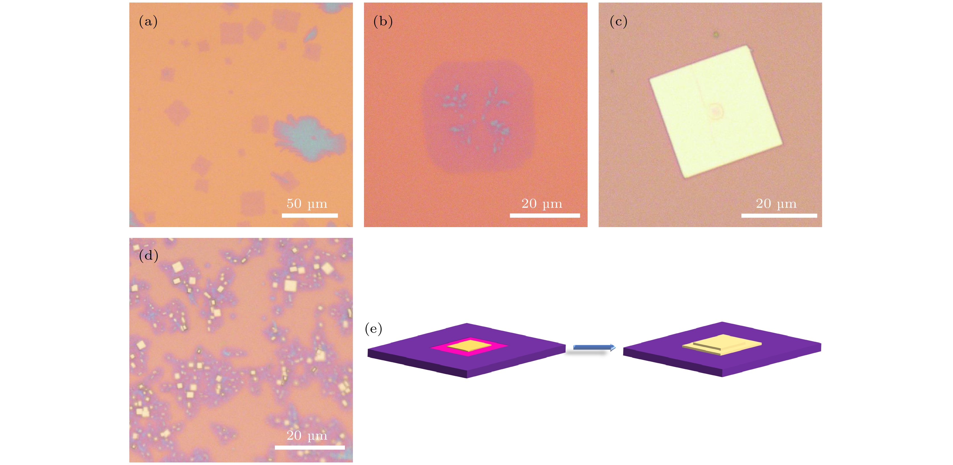
图 2 光学表征与生长机理 (a)薄层Bi2O2Se的低倍光学照片;(b)薄层Bi2O2Se的高倍光学照片; (c)多层Bi2O2Se光学照片; (d) 多层样品以薄层样品作为基底生长的光学照片; (e) 生长台阶状样品可能的机理示意图
Fig. 2. Optical characterization and growth mechanism: (a) Optical image of thin-layer Bi2O2Se with low magnification; (b) optical image of thin-layer Bi2O2Se with high magnification; (c) optical image of multilayer Bi2O2Se; (d) optical image showing thin-layer sample as growth substrate of multilayer sample; (e) possible growth mechanism of stepped sample.

图 3 Bi2O2Se的表征 (a) Raman光谱; (b)和(c) AFM表征; (d) 拓扑高度曲线显示台阶样品厚度约为51 nm; (e) SEM照片; (f) EDS 图谱
Fig. 3. Characterization of Bi2O2Se: (a) Raman spectrum; (b) and (c) AFM characterization; (d) topography height profile revealing the thickness of the stepped sample is about 51.0 nm; (e) SEM image; (f) EDS spectrum.
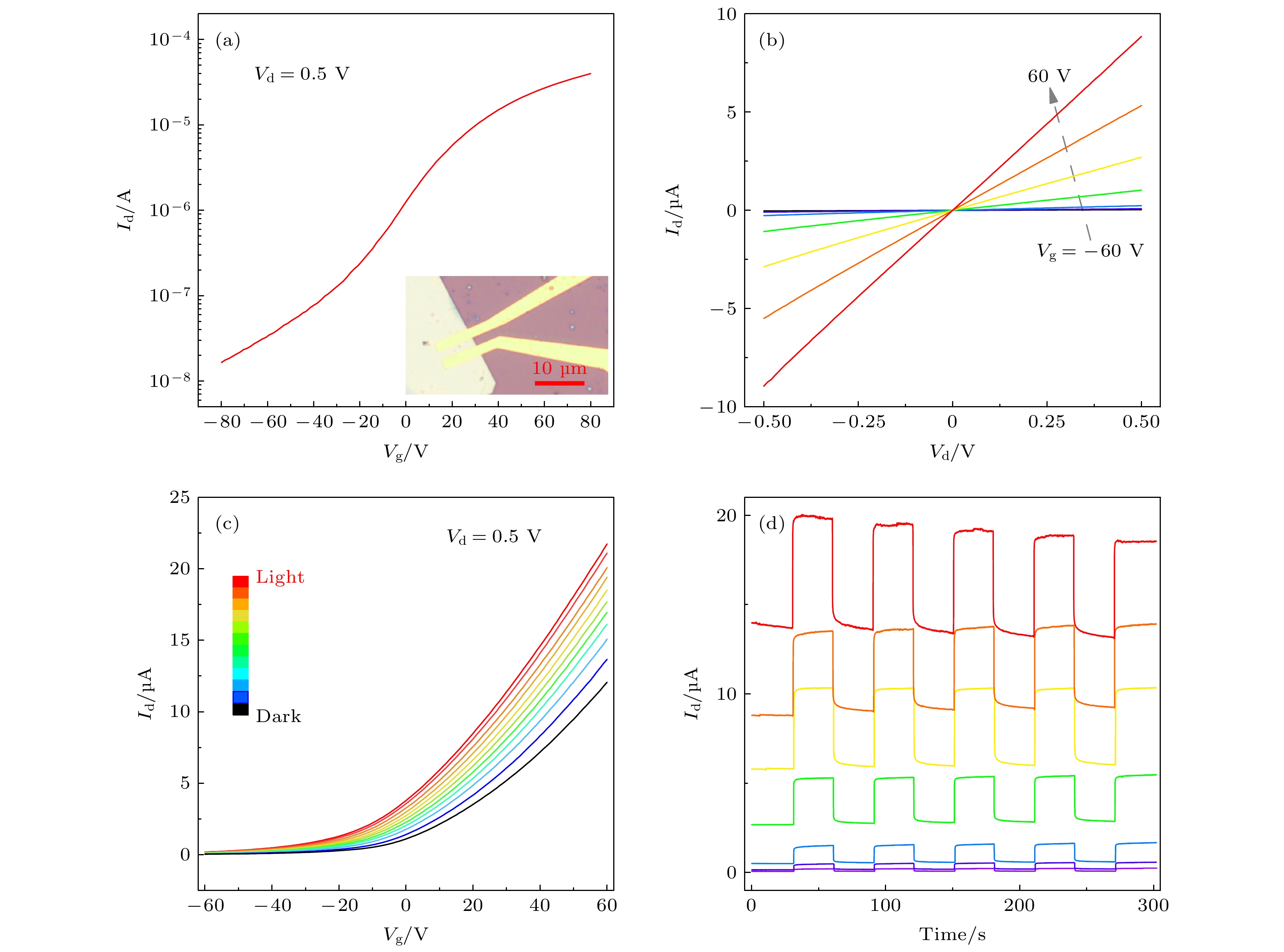
图 4 Bi2O2Se的FET及光电响应 (a) FET的Id-Vg曲线, 插图为FET器件的光学图片; (b) FET的Id-Vd曲线; (c)晶体管光电响应的Id-Vg曲线; (d) 光电晶体管光电开关响应的Id-t曲线
Fig. 4. FET and Phototransistor performance of Bi2O2Se: (a) FET Id-Vg curve, inset is optical image of FET device; (b) FET Id-Vd curve; (c) phototransistor Id-Vg curve; (d) phototransistor on/off sensing Id-t curve.
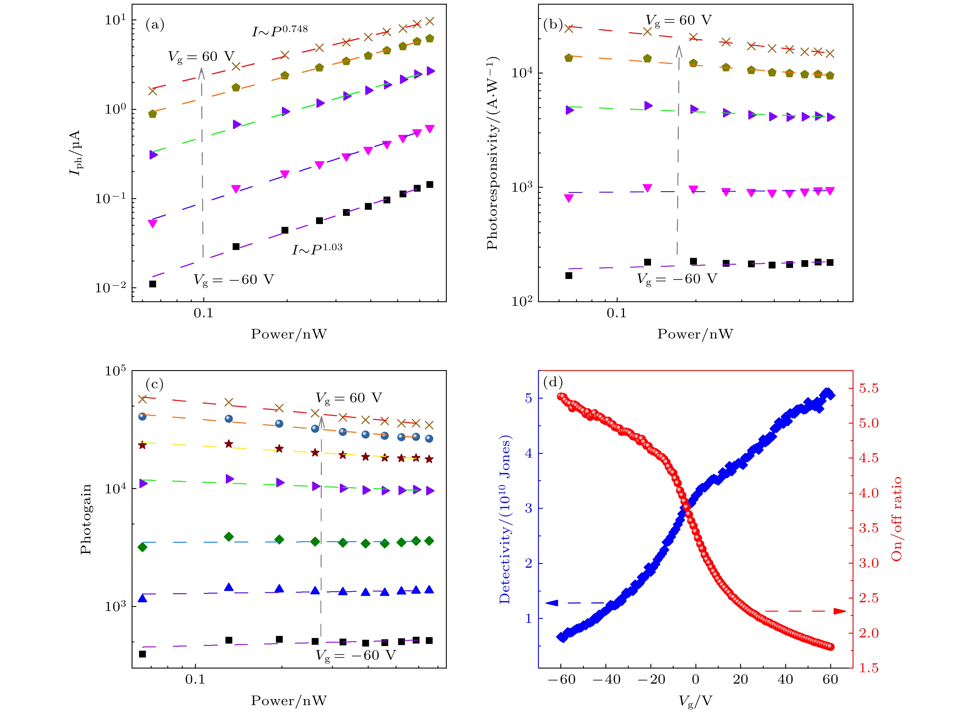
图 5 Bi2O2Se光电晶体管性能分析 (a) 不同栅压下, Iph与光强的关系; (b) 不同栅压下, 光响应度与光强的关系; (c) 不同栅压下, 光增益与光强的关系; (d) 光检测灵敏度以及开关比与栅压的关系
Fig. 5. Analysis of Bi2O2Se phototransistor data: (a) The relationship of photocurrent(Iph) with light source power under different backgate voltages; (b) the relationship of photoresponsivity (R) with light source power under different backgate voltages; (c) the relationship of photogain(G) with light source power under different backgate voltages; (d) the relationship of detectivity(D) and on/off ratio with backgate voltage.
-
[1] 2021 IRDS Lithography Report
[2] Winstead B, Ravaioli U 2000 IEEE T. Electron Dev. 47 1241
Google Scholar
[3] Hooper W, Lehrer W 1967 Proc. IEEE 55 1237
Google Scholar
[4] Sze S, Irvin J 1968 Solid-State Electron. 11 599
Google Scholar
[5] Asif Khan M, Kuznia J, Bhattarai A, Olson D 1993 Appl. Phys. Lett. 62 1786
Google Scholar
[6] Novoselov K S, Jiang D, Schedin F, Booth T J, Khotkevich V V, Morozov S V, Geim A K 2005 Proc. Natl. Acad. Sci. U S A 102 10451
Google Scholar
[7] Lee Y H, Zhang X Q, Zhang W, Chang M T, Lin C T, Chang K D, Yu Y C, Wang J T, Chang C S, Li L J, Lin T W 2012 Adv. Mater. 24 2320
Google Scholar
[8] Zhan Y, Liu Z, Najmaei S, Ajayan P M, Lou J 2012 Small 8 966
Google Scholar
[9] Duan X, Wang C, Shaw J C, Cheng R, Chen Y, Li H, Wu X, Tang Y, Zhang Q, Pan A 2014 Nat. Nanotechnol. 9 1024
Google Scholar
[10] Li L, Yu Y, Ye G J, Ge Q, Ou X, Wu H, Feng D, Chen X H, Zhang Y 2014 Nat. Nanotechnol. 9 372
Google Scholar
[11] Novoselov K S, Geim A K, Morozov S V, Jiang D, Zhang Y, Dubonos S V, Grigorieva I V, Firsov A A 2004 Science 306 666
Google Scholar
[12] Radisavljevic B, Radenovic A, Brivio J, Giacometti V, Kis A 2011 Nat. Nanotechnol. 6 147
Google Scholar
[13] Li W, Zhou J, Cai S, Yu Z, Zhang J, Fang N, Li T, Wu Y, Chen T, Xie X 2019 Nat. Electron. 2 563
Google Scholar
[14] Cronemeyer D C 1957 Phys. Rev. 105 522
Google Scholar
[15] Bandurin D A, Tyurnina A V, Geliang L Y, Mishchenko A, Zólyomi V, Morozov S V, Kumar R K, Gorbachev R V, Kudrynskyi Z R, Pezzini S 2017 Nat. Nanotechnol. 12 223
Google Scholar
[16] Chow W L, Yu P, Liu F, Hong J, Wang X, Zeng Q, Hsu C H, Zhu C, Zhou J, Wang X 2017 Adv. Mater. 29 1602969
Google Scholar
[17] Zhao Y, Qiao J, Yu Z, Yu P, Xu K, Lau S P, Zhou W, Liu Z, Wang X, Ji W 2017 Adv. Mater. 29 1604230
Google Scholar
[18] Wu J, Liu Y, Tan Z, Tan C, Yin J, Li T, Tu T, Peng H 2017 Adv. Mater. 29 1704060
Google Scholar
[19] Wu J, Tan C, Tan Z, Liu Y, Yin J, Dang W, Wang M, Peng H 2017 Nano Lett. 17 3021
Google Scholar
[20] Wu J, Yuan H, Meng M, Chen C, Sun Y, Chen Z, Dang W, Tan C, Liu Y, Yin J 2017 Nat. Nanotechnol. 12 530
Google Scholar
[21] Li T, Peng H 2021 Acc. Mater. Res. 2 842
Google Scholar
[22] Tan C, Tang M, Wu J, Liu Y, Li T, Liang Y, Deng B, Tan Z, Tu T, Zhang Y 2019 Nano Lett. 19 2148
Google Scholar
[23] Fu Q, Zhu C, Zhao X, Wang X, Chaturvedi A, Zhu C, Wang X, Zeng Q, Zhou J, Liu F 2019 Adv. Mater. 31 1804945
Google Scholar
[24] Seu K J, Pandey A P, Haque F, Proctor E A, Ribbe A E, Hovis J S 2007 Biophys. J. 92 2445
Google Scholar
[25] Liu Y, Guo J, Zhu E, Liao L, Lee S-J, Ding M, Shakir I, Gambin V, Huang Y, Duan X 2018 Nature 557 696
Google Scholar
[26] Grinvald A, Steinberg I Z 1974 Anal. Biochem. 59 583
Google Scholar
[27] Furchi M M, Polyushkin D K, Pospischil A, Mueller T 2014 Nano Lett. 14 6165
Google Scholar
[28] Gong X, Tong M, Xia Y, Cai W, Moon J S, Cao Y, Yu G, Shieh C-L, Nilsson B, Heeger A J 2009 Science 325 1665
Google Scholar
[29] Liu S, Wei Z, Cao Y, Gan L, Wang Z, Xu W, Guo X, Zhu D 2011 Chem. Sci. 2 796
Google Scholar


 下载:
下载:


计量
- 文章访问数: 8473
- PDF下载量: 333
- 被引次数: 0
