


-
硅光电倍增管(SiPM)在微弱光探测领域已获得广泛应用. 然而基于小尺寸G-APD单元的SiPM存在有效几何填充因子(GFF)受限问题, 使其光子探测效率(PDE)相对较低. 此外, 受硅材料本征特性制约, 其在近红外波段的PDE亦相对不足. 针对上述问题, 本文提出一种基于拓扑光子晶体(TPC)的分区域光场调控方案, 旨在不改变SiPM内部结构的前提下提升其PDE. 通过COMSOL电磁波频域仿真, 揭示了死区拓扑边缘态引导、光敏区慢光效应及布拉格散射的多波段协同机制: 在460—700 nm波段, 死区蜂窝晶格通过Floquet周期性分析诱导拓扑边缘态, 同时利用晶格周期性介电分布激发布拉格散射, 减少光子在金属表面的反射损耗, 将光子精准耦合至光敏区, 其在621 nm处的有效GFF从46.4%提升至63.1%; 在700—1100 nm波段, 除布拉格散射减少反射损耗外, 所设计的周期性硅柱结构可通过慢光效应有效延长光子横向传播路径, 进而提升与光敏区耦合概率, 其在900 nm处的吸收效率由41.19%显著提升至55.94%. 仿真结果表明, 该设计方案使SiPM在460—1100 nm波段PDE平均提升50% (峰值达81%), 可以通过主流的刻蚀工艺(电子束光刻+反应离子刻蚀)实现. 与传统微透镜及等离激元结构相比, TPC在宽光谱响应与工艺简化方面具有显著优势. 本研究为SiPM的光子回收与PDE增强提供了拓扑光子学新路径.Silicon photomultipliers (SiPMs) have been widely used in the field of weak light detection. However, SiPMs utilizing small-sized Geiger-mode avalanche photodiode (G-APD) cells face the limitations due to a restricted effective geometric fill sactor (GFF), which leads to relatively low photon detection efficiency (PDE), and additionally, constrained by the intrinsic properties of silicon materials, their PDE in the near-infrared band is also relatively insufficient. To address the above issues, this work proposes a regional optical field modulation approach based on topological photonic crystals (TPCs), aiming to improve the PDE of SiPMs without modifying their internal structure. Through COMSOL electromagnetic wave frequency-domain simulation, the multi-band synergistic mechanism of dead-zone topological edge state guidance, photosensitive region slow-light effect, and Bragg scattering is revealed. In the 460–700 nm band, the honeycomb lattice in the dead zone induces topological edge states via Floquet periodic analysis, while the periodic dielectric distribution of the lattice excites Bragg scattering to reduce photon reflection loss at the metal surface and precisely couples photons to the photosensitive region, leading to an increase in effective GFF from 46.4% to 63.1% at 621 nm. In the 700–1100 nm band, in addition to reducing reflection loss via Bragg scattering, the designed periodic silicon pillar structure can effectively extend the transverse propagation path of photons through the slow-light effect, thereby increasing the coupling probability with the photosensitive region, resulting in a significant increase in absorption efficiency from 41.19% to 55.94% at 900 nm. Simulation results show that this design scheme increases the average PDE of SiPMs by 50% in the 460–1100 nm band (with a peak value of 81%) and can be implemented via mainstream etching processes (electron beam lithography + reactive ion etching). Compared with traditional microlens and plasmonic structures, TPCs exhibit significant advantages in broad-spectrum response and process simplification. This work provides a new topological photonics approach for photon recycling and PDE enhancement of SiPMs.
-
Keywords:
- silicon photomultiplier /
- photon detection efficiency /
- topological photonic crystal /
- slow-light effect
[1] Zhao B, Huang Y, Wang C 2024 Nucl. Instrum. Methods Phys. Res. Sect. A 1059 168975
 Google Scholar
[2] Rignanese L P, Antonioli P, Preghenella R, Scapparone E 2024 La Riv. Nuovo Cimento 47 299
Google Scholar
[3] Herbert D J, Saveliev V, Belcari N, Bisogni M G, Del Guerra A, Golovin A 2004 IEEE Nuclear Science Symposium Conference Record Rome, Italy, October 16–22, 2004 p4185
[4] Yan T Y, Wang X Y, Liu S T, Fan D W, Xu X Y, Zeng Q, Xie H, Yang X L, Zhu S P, Ma X P, Yuan Z, Chen X L 2022 Small Methods 6 2201105
Google Scholar
[5] Okino T, Yamada S, Sakata Y, Kasuga S, Takemoto M, Nose Y, Koshida H, Tamaru M, Sugiura Y, Saito S, Koyama S, Mori M, Hirose Y, Sawada M, Odagawa A, Tanaka T 2020 IEEE International Solid-State Circuits Conference (ISSCC) San Francisco, CA, USA, February 16–20, 2020 p9063045
[6] Baker-Finch S C, McIntosh K R, Yan D, Fong K C, Kho T C 2014 J. Appl. Phys. 116 063101
Google Scholar
[7] Haefeli G, Blanc F, Currás-Rivera E, Marchevski R, Ronchetti F, Schneider O, Shchutska L, Trippl C, Zaffaroni E, Zunica G 2024 arXiv: 2411.09358 [hep-ex]
[8] Álvarez-Garrote R, Calvo E, Canto A, Crespo-Anadón J I, Cuesta C, de la Torre Rojo A, Gil-Botella I, Manthey Corchado S, Martín I, Palomares C, Pérez-Molina L, Verdugo de Osa A 2024 Nucl. Instrum. Methods Phys. Res. Sect. A 1064 169347
Google Scholar
[9] Villa F, Bronzi D, Vergani M, Zou Y, Ruggeri A, Zappa F, Dalla Mora A 2014 European Solid-State Device Research Conference (ESSDERC) Grenoble, France, September 22–26, 2014 p294
[10] Wang Y, Chen Z D, Li C H, He R, Wang S Y, Li B C, Wang R H, Liang K, Yang R, Han D J 2015 Nucl. Instrum. Methods Phys. Res., Sect. A 787 38
Google Scholar
[11] 贾鼎, 葛勇, 袁寿其, 孙宏祥 2019 68 224301
Google Scholar
Jia D, Ge Y, Yuan S Q, Sun H X 2019 Acta Phys. Sin. 68 224301
Google Scholar
[12] 鲁辉, 田慧平, 李长红, 纪越峰 2009 58 2049
Google Scholar
Lu H, Tian H P, Li C H, Ji Y F 2009 Acta Phys. Sin. 58 2049
Google Scholar
[13] Wu L H, Hu X 2015 Phys. Rev. Lett. 114 223901
Google Scholar
[14] 崔昊杨, 李志锋, 马法君, 陈效双, 陆卫 2010 59 7055
Google Scholar
Cui H Y, Li Z F, Ma F J, Chen X S, Lu W 2010 Acta Phys. Sin. 59 7055
Google Scholar
[15] Xiao L, Lei T Y, Liang Y, Zhao M, Liu H, Zhang S Q, Li H, Ma J, Wu X Y 2016 Acta Phys. Sin. 65 134207 [肖利, 雷天宇, 梁禺, 赵敏, 刘慧, 张斯淇, 李宏, 马季, 吴向尧 2016 65 134207]
Google Scholar
Xiao L, Lei T Y, Liang Y, Zhao M, Liu H, Zhang S Q, Li H, Ma J, Wu X Y 2016 Acta Phys. Sin. 65 134207
Google Scholar
[16] 赵聪, 马颖, 汪洋, 周雪, 李会增, 李明珠, 宋延林 2018 化学学报 76 9
Google Scholar
Zhao C, Ma Y, Wang Y, Zhou X, Li H Z, Li M Z, Song Y L 2018 Acta Chim. Sin. 76 9
Google Scholar
[17] Zou S W, Xin Y, Jin J L, Lin Z C, He Y Y, Liang J, Yan X J, Huang J M 2025 Adv. Mater. 37 2410130
Google Scholar
[18] Wang Y, Yang Y F, Wu Y, Wang L, Liu L, Liu L N, Li L B, Han X X, Li Z B, Zhang G Q 2024 Proceedings of SPIE San Diego, CA, USA, August 12–16, 2024 p13283
[19] 郑煜, 郜飘飘, 唐昕, 李静, 刘洋, 张浩 2022 中南大学学报 29 3335
Google Scholar
Zheng Y, Gao P P, Tang X, Li J, Liu Y, Zhang H 2022 J. Cent. South Univ. 29 3335
Google Scholar
[20] 毛姗姗, 李艳秋, 姜家华, 沈诗欢, 刘克, 郑猛 2018 中国光学快报 16 030801
Google Scholar
Mao S S, Li Y Q, Jiang J H, Shen S H, Liu K, Zheng M 2018 Chin. Opt. Lett. 16 030801
Google Scholar
[21] Zhou W M, Min G Q, Zhang J, Liu Y B, Wang J H, Zhang Y P, Sun F 2011 Nano-Micro Lett. 3 135
Google Scholar
[22] Gyongy I, Davies A, Gallinet B, Dutton N A W, Duncan R R, Rickman C, Henderson R K, Dalgarno P A 2018 Opt. Express 26 2280
Google Scholar
[23] Intermite G, McCarthy A, Warburton R E, Ren X, Villa F, Lussana R, Waddie A J, Taghizadeh M R, Tosi A, Zappa F, Buller G S 2015 Opt. Express 23 33777
Google Scholar
[24] Duan Q L, Liu Y, Chang S S, Chen H Y, Chen J H 2021 Sensors 21 5262
Google Scholar
-

图 1 SiPM表面构建拓扑光子晶体原理示意图 (a) SiPM三维结构示意图; (b) 近距离俯视图; (c) 拓扑绝缘光子晶体示意图(近距离); (d) 表面具有拓扑光子晶体的SiPM二维剖面示意图; (e) TPC二维晶格示意图; (f) Floquet周期性分析示意图; (g) 光子在TPC中传播示意图
Fig. 1. Schematic diagrams of the principle of constructing topological photonic crystals on the surface of SiPM: (a) Schematic diagram of the three-dimensional structure of SiPM; (b) close-up top view; (c) schematic diagram of topological insulating photonic crystal (close-up); (d) two-dimensional cross-sectional schematic diagram of SiPM with topological photonic crystals on the surface; (e) schematic diagram of TPC two-dimensional lattice; (f) schematic diagram of Floquet periodicity analysis; (g) schematic diagram of photon propagation in TPC.
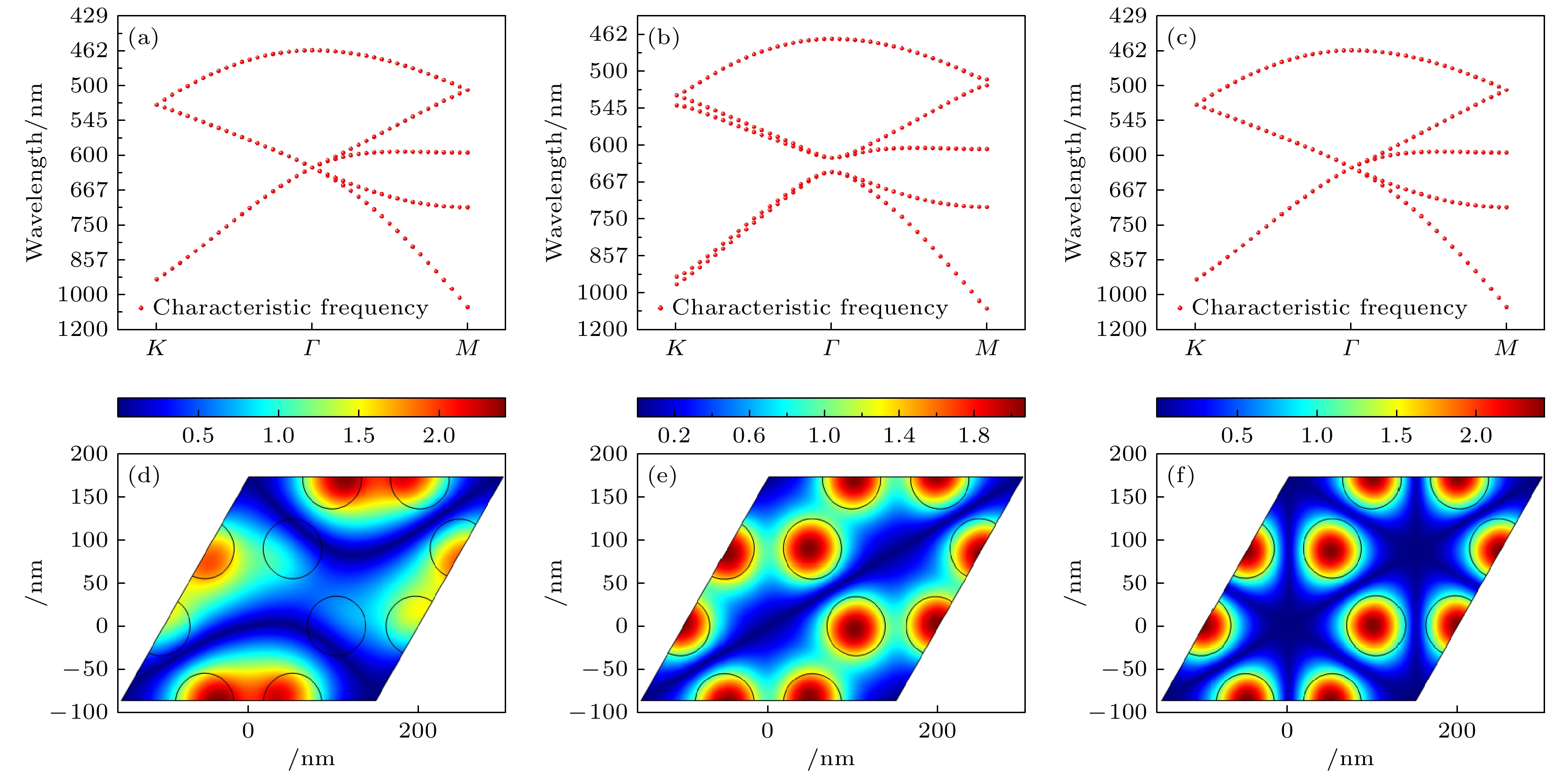
图 2 拓扑绝缘光子晶体单个晶格结构的能带图 (a) R = a0/3; (b) R = a0/2.9; (c) R = a0/3.1; (d) 边界态; (e) 布拉格散射体态; (f) 纯体态电场模分布(单位: V)
Fig. 2. Energy band diagrams of a single lattice structure of topological insulating photonic crystals: (a) R = a0/3; (b) R = a0/2.9; (c) R = a0/3.1; (d) boundary state; (e) Bragg scattering bulk state; (f) electric field mode distribution of pure bulk state (unit: V).

图 3 三维仿真结构图 (a) 几何建模; (b) 光子晶体电场模分布(单位: V)
Fig. 3. Three-dimensional simulation structure diagrams: (a) Geometric modeling; (b) electric field mode distribution of photonic crystals (unit: V).
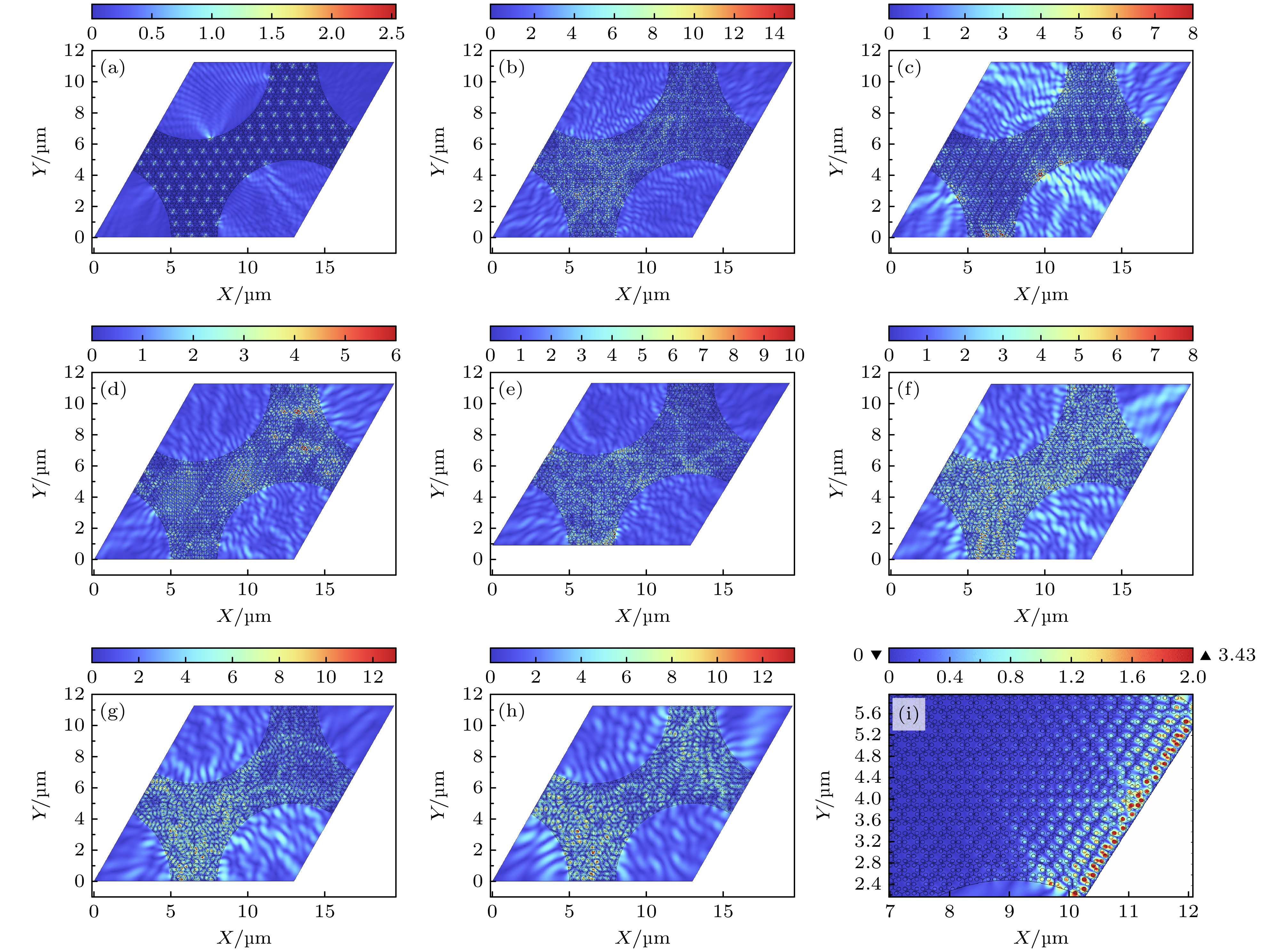
图 4 不同波长下死区构建TPC的电场模分布图(单位: V) (a) 450 nm; (b) 550 nm; (c) 621 nm; (d) 650 nm; (e) 700 nm; (f) 800 nm; (g) 900 nm; (h) 1100 nm; (i) 621 nm波长下的边界态传播
Fig. 4. Electric field mode distribution diagrams of TPC constructed in the dead zone (unit: V) at different wavelengths: (a) 450 nm; (b) 550 nm; (c) 621 nm; (d) 650 nm; (e) 700 nm; (f) 800 nm; (g) 900 nm; (h) 1100 nm; (i) boundary state propagation at 621 nm wavelength.

图 5 不同波长下光敏区构建TPC的电场模分布图(单位: V) (a) 460 nm; (b) 550 nm; (c) 650 nm; (d) 700 nm; (e) 900 nm; (f) 1100 nm
Fig. 5. Electric field mode distribution diagrams of TPC constructed in the photosensitive region (unit: V) at different wavelengths: (a) 460 nm; (b) 550 nm; (c) 650 nm; (d) 700 nm; (e) 900 nm; (f) 1100 nm.

图 7 表面有无拓扑光子晶体结构的SiPM的PDE曲线对比
Fig. 7. Comparison of PDE curves of SiPM with and without surface topological photonic crystal structure.
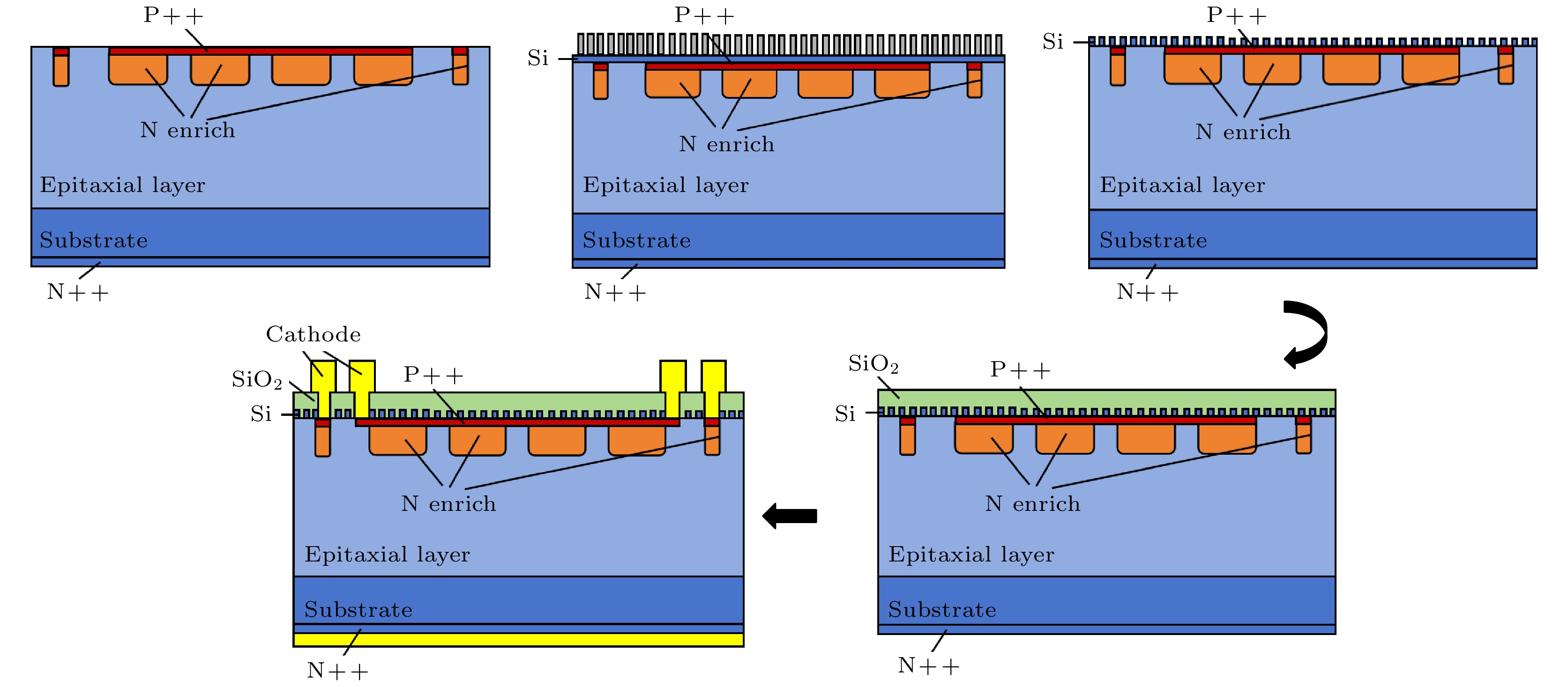
图 8 表面集成TPC的SiPM制作工艺流程图
Fig. 8. Flow chart of the manufacturing process of SiPM with surface-integrated TPC.
表 2 硅柱直径刻蚀误差对SiPM PDE的影响
Table 2. Influences of silicon pillar diameter etching errors on SiPM PDE.
硅柱直径
偏差621 nm处
有效GFF/%900 nm处
吸收效率/%460—1100 nm波段
PDE 平均提升/%无误差
(原设计)63.10 51.37 50 ±5 nm 61.46 49.85 48.5 ±10 nm 59.29 48.27 46.8  下载: 导出CSV
-
[1] Zhao B, Huang Y, Wang C 2024 Nucl. Instrum. Methods Phys. Res. Sect. A 1059 168975
Google Scholar
[2] Rignanese L P, Antonioli P, Preghenella R, Scapparone E 2024 La Riv. Nuovo Cimento 47 299
Google Scholar
[3] Herbert D J, Saveliev V, Belcari N, Bisogni M G, Del Guerra A, Golovin A 2004 IEEE Nuclear Science Symposium Conference Record Rome, Italy, October 16–22, 2004 p4185
[4] Yan T Y, Wang X Y, Liu S T, Fan D W, Xu X Y, Zeng Q, Xie H, Yang X L, Zhu S P, Ma X P, Yuan Z, Chen X L 2022 Small Methods 6 2201105
Google Scholar
[5] Okino T, Yamada S, Sakata Y, Kasuga S, Takemoto M, Nose Y, Koshida H, Tamaru M, Sugiura Y, Saito S, Koyama S, Mori M, Hirose Y, Sawada M, Odagawa A, Tanaka T 2020 IEEE International Solid-State Circuits Conference (ISSCC) San Francisco, CA, USA, February 16–20, 2020 p9063045
[6] Baker-Finch S C, McIntosh K R, Yan D, Fong K C, Kho T C 2014 J. Appl. Phys. 116 063101
Google Scholar
[7] Haefeli G, Blanc F, Currás-Rivera E, Marchevski R, Ronchetti F, Schneider O, Shchutska L, Trippl C, Zaffaroni E, Zunica G 2024 arXiv: 2411.09358 [hep-ex]
[8] Álvarez-Garrote R, Calvo E, Canto A, Crespo-Anadón J I, Cuesta C, de la Torre Rojo A, Gil-Botella I, Manthey Corchado S, Martín I, Palomares C, Pérez-Molina L, Verdugo de Osa A 2024 Nucl. Instrum. Methods Phys. Res. Sect. A 1064 169347
Google Scholar
[9] Villa F, Bronzi D, Vergani M, Zou Y, Ruggeri A, Zappa F, Dalla Mora A 2014 European Solid-State Device Research Conference (ESSDERC) Grenoble, France, September 22–26, 2014 p294
[10] Wang Y, Chen Z D, Li C H, He R, Wang S Y, Li B C, Wang R H, Liang K, Yang R, Han D J 2015 Nucl. Instrum. Methods Phys. Res., Sect. A 787 38
Google Scholar
[11] 贾鼎, 葛勇, 袁寿其, 孙宏祥 2019 68 224301
Google Scholar
Jia D, Ge Y, Yuan S Q, Sun H X 2019 Acta Phys. Sin. 68 224301
Google Scholar
[12] 鲁辉, 田慧平, 李长红, 纪越峰 2009 58 2049
Google Scholar
Lu H, Tian H P, Li C H, Ji Y F 2009 Acta Phys. Sin. 58 2049
Google Scholar
[13] Wu L H, Hu X 2015 Phys. Rev. Lett. 114 223901
Google Scholar
[14] 崔昊杨, 李志锋, 马法君, 陈效双, 陆卫 2010 59 7055
Google Scholar
Cui H Y, Li Z F, Ma F J, Chen X S, Lu W 2010 Acta Phys. Sin. 59 7055
Google Scholar
[15] Xiao L, Lei T Y, Liang Y, Zhao M, Liu H, Zhang S Q, Li H, Ma J, Wu X Y 2016 Acta Phys. Sin. 65 134207 [肖利, 雷天宇, 梁禺, 赵敏, 刘慧, 张斯淇, 李宏, 马季, 吴向尧 2016 65 134207]
Google Scholar
Xiao L, Lei T Y, Liang Y, Zhao M, Liu H, Zhang S Q, Li H, Ma J, Wu X Y 2016 Acta Phys. Sin. 65 134207
Google Scholar
[16] 赵聪, 马颖, 汪洋, 周雪, 李会增, 李明珠, 宋延林 2018 化学学报 76 9
Google Scholar
Zhao C, Ma Y, Wang Y, Zhou X, Li H Z, Li M Z, Song Y L 2018 Acta Chim. Sin. 76 9
Google Scholar
[17] Zou S W, Xin Y, Jin J L, Lin Z C, He Y Y, Liang J, Yan X J, Huang J M 2025 Adv. Mater. 37 2410130
Google Scholar
[18] Wang Y, Yang Y F, Wu Y, Wang L, Liu L, Liu L N, Li L B, Han X X, Li Z B, Zhang G Q 2024 Proceedings of SPIE San Diego, CA, USA, August 12–16, 2024 p13283
[19] 郑煜, 郜飘飘, 唐昕, 李静, 刘洋, 张浩 2022 中南大学学报 29 3335
Google Scholar
Zheng Y, Gao P P, Tang X, Li J, Liu Y, Zhang H 2022 J. Cent. South Univ. 29 3335
Google Scholar
[20] 毛姗姗, 李艳秋, 姜家华, 沈诗欢, 刘克, 郑猛 2018 中国光学快报 16 030801
Google Scholar
Mao S S, Li Y Q, Jiang J H, Shen S H, Liu K, Zheng M 2018 Chin. Opt. Lett. 16 030801
Google Scholar
[21] Zhou W M, Min G Q, Zhang J, Liu Y B, Wang J H, Zhang Y P, Sun F 2011 Nano-Micro Lett. 3 135
Google Scholar
[22] Gyongy I, Davies A, Gallinet B, Dutton N A W, Duncan R R, Rickman C, Henderson R K, Dalgarno P A 2018 Opt. Express 26 2280
Google Scholar
[23] Intermite G, McCarthy A, Warburton R E, Ren X, Villa F, Lussana R, Waddie A J, Taghizadeh M R, Tosi A, Zappa F, Buller G S 2015 Opt. Express 23 33777
Google Scholar
[24] Duan Q L, Liu Y, Chang S S, Chen H Y, Chen J H 2021 Sensors 21 5262
Google Scholar


 下载:
下载:


计量
- 文章访问数: 1108
- PDF下载量: 58
- 被引次数: 0
