


-
The directional optical transmission characteristics of on-chip integrated optical isolators have wide applications in fields such as optical communication and optical signal processing. At early stage, various schemes of on-chip optical isolators have been developed, such as single-crystal magneto-optical pomegranate scheme, and silicon nitride (Si3N4) micro-ring resonators. However, there is still lack of compact on-chip optical isolator solutions. Here, a compact and integrated silicon optical isolator on a standard silicon on insulator (SOI) substrate is proposed and designed by intelligent algorithms and a variety of micro-nano circular vias. A modified genetic algorithm is developed, a segmented design fitness function is induced, and a gene library is established to obtain an ultra-compact optical isolator scheme with a size of only 4.2 μm×3 μm. On a standard silicon on insulator substrate, a linear passive isolation scheme is achieved by etching circular holes with five different diameters: 60 nm, 120 nm, 180 nm, 240 nm, and 300 nm. In the TE polarization mode, the design achieves an isolation degree of approximately 31 dB and an insertion loss of about 2 dB. Furthermore, in TM polarization mode, the design achieves an isolation degree of approximately 38 dB and an insertion loss of 2 dB; Finally, the influence of different size groups on the performance of isolators is analyzed. The results show that the smaller the circular hole structure, the better the isolation performance is. However, at the same time, we also need to consider the real silicon etching process requirements. In practice, holes that are too small are difficult to etch the effects of etching penetration at 10 nm, 20 nm and 30 nm between circular vias on the performance of the isolator are also evaluated, and the preliminary results show that the etching penetration caused by the more mature 30 nm etching process is acceptable. Therefore, considering all factors, it is recommended that the minimum circular hole size be 30 nm and the minimum distance adjacent circular holes be 30 nm. These results can promote the development of highly integrated and ultra-small on-chip optical signal directional transmission schemes.
-
Keywords:
- integrated optical isolator /
- ultra-compact /
- genetic algorithms
[1] Yu M, Cheng R, Reimer C, He L, Luke K, Puma E, Shao L, Shams-Ansari A, Ren X, Grant H R, Johansson L, Zhang M, Lončar M 2023 Nat. Photonics 17 666
 Google Scholar
[2] Huang D, Pintus P, Shoji Y, Morton P, Mizumoto T, Bowers J E 2017 Opt. Lett. 42 23
Google Scholar
[3] Pintus P, Huang D, Zhang C, Shoji Y, Mizumoto T, Bowers J E 2017 J. Lightwave Technol. 35 1429
Google Scholar
[4] Bi L, Hu J, Jiang P, Kim D H, Dionne G F, Kimerling L C, Ross C 2011 Nat. Photonics 5 758
Google Scholar
[5] Onbasli M C, Beran L, Zahradník M, Kučera M, Antoš R, Mistrík J, Dionne G F, Veis M, Ross C A 2016 Sci. Rep. 6 23640
Google Scholar
[6] White A D, Ahn G H, Gasse K V, Yang K Y, Chang L, Bowers J E, Vučković J 2023 Nat. Photonics 17 143
Google Scholar
[7] Abdelsalam K, Li T, Khurgin J B, Fathpour S 2020 Optica 7 209
Google Scholar
[8] Dostart N, Gevorgyan H, Onural D, Popović M A 2021 Opt. Lett. 46 460
Google Scholar
[9] Lira H, Yu Z, Fan S, Lipson M 2012 Phys. Rev. Lett. 109 033901
Google Scholar
[10] Herrmann J F, Ansari V, Wang J, Witmer J D, Fan S, Safavi-Naeini A H 2022 Nat. Photonics 16 603
Google Scholar
[11] Yu Z, Fan S 2009 Nat. Photonics 3 91
Google Scholar
[12] Kang M S, Butsch A, Russell P S J 2011 Nat. Photonics 5 549
Google Scholar
[13] Wang C, Zhou C Z, Li Z Y 2011 Opt. Express 19 26948
Google Scholar
[14] Wang C, Zhong X L, Li Z Y 2012 Sci. Rep. 2 674
Google Scholar
[15] Mizumoto T, Shoji Y 2020 Optical Fiber Communication Conference (OFC) 2020 San Diego, California, United States, March 8–12, 2020 pT3B.1
[16] Karki D, Stenger V, Pollick A, Levy M 2020 J. Lightwave Technol. 38 827
Google Scholar
[17] Tian H, Liu J, Siddharth A, Wang R N, Blésin T, He J, Kippenberg T J, Bhave S A 2021 Nat. Photonics 15 828
Google Scholar
[18] Seldowitz M A, Allebach J P, Sweeney D W 1987 Appl. Opt. 26 2788
Google Scholar
[19] Yuan H, Wu J, Zhang J, Pu X, Zhang Z, Yu Y, Yang J 2022 Nanomaterials 12 669
Google Scholar
[20] Peng Z, Feng J, Yuan H, et al. 2022 Nanomaterials 12 1121
Google Scholar
[21] Lalau-Keraly C M, Bhargava S, Miller O D, Yablonovitch E 2013 Opt. Express 21 21693
Google Scholar
[22] Keraly C L, Bhargava S, Ganapati V, et al. 2014 CLEO: Science and Innovations 2014 San Jose, California, United States, June 8–13, 2014 pSTu2 M.6
[23] Liao J, Tian Y, Yang Z, Xu H, Tang C, Wang Y, Zhang X, Kang Z 2024 Chin. Opt. Lett. 22 011302
Google Scholar
[24] Wang Z, Feng J, Li H, Zhang Y, Wu Y, Hu Y, Wu J, Yang J 2023 Nanomaterials 13 2516
Google Scholar
[25] Piggott A Y, Lu J, Lagoudakis K G, Petykiewicz J, Babinec T M, Vučković J 2015 Nat. Photonics 9 374
Google Scholar
[26] Nanda A, Kues M, Calà Lesina A 2024 Opt. Lett. 49 1125
Google Scholar
[27] Vercruysse D, Sapra N V, Su L, Trivedi R, Vučković J 2019 Sci. Rep. 9 8999
Google Scholar
[28] Cao J, Zhao Z, Sun H, Yang Y, Deng Y, Cao P 2023 J. Phys.: Conf. Ser. 2464 012019
Google Scholar
[29] Mak J C, Sideris C, Jeong J, Hajimiri A, Poon J K 2016 Opt. Lett. 41 3868
Google Scholar
[30] Yao R, Li H, Zhang B, Chen W, Wang P, Dai S, Liu Y, Li J, Li Y, Fu Q, Dai T, Yu H, Yang J, Pavesi L 2021 J. Lightwave Technol. 39 6253
Google Scholar
[31] Lee I, Kim C, Ju K, Jun G, Yoon G 2023 Appl. Opt. 62 8994
Google Scholar
[32] Jia W, Jiang L, Li X 2010 Opt. Commun. 283 1537
Google Scholar
[33] Yu Z, Cui H, Sun X 2017 Opt. Lett. 42 3093
Google Scholar
[34] Mirzaei A, Miroshnichenko A E, Shadrivov I V, Kivshar Y S 2014 Appl. Phys. Lett. 105 011109
Google Scholar
[35] Wang Z, Peng Z, Zhang Y, Wu Y, Hu Y, Wu J, Yang J 2023 Opt. Express 31 15904
Google Scholar
[36] Peng Z, Feng J, Du T, Cheng W, Wang Y, Zang S, Cheng H, Ren X, Shuai Y, Liu H, Wu J, Yang J 2022 Opt. Express 30 27366
Google Scholar
[37] Cakirlar C, Galderisi G, Beyer C, Simon M, Mikolajick T, Trommer J 2022 2022 IEEE 22nd International Conference on Nanotechnology (NANO) Palma de Mallorca, Spain, July 4–8, 2022 pp207–210
[38] Saifullah M, Subramanian K, Tapley E, Kang D J, Welland M, Butler M 2003 Nano Lett. 3 1587
Google Scholar
[39] Wang K, Ren X, Chang W, Lu L, Liu D, Zhang M 2020 Photonics Res. 8 528
Google Scholar
-
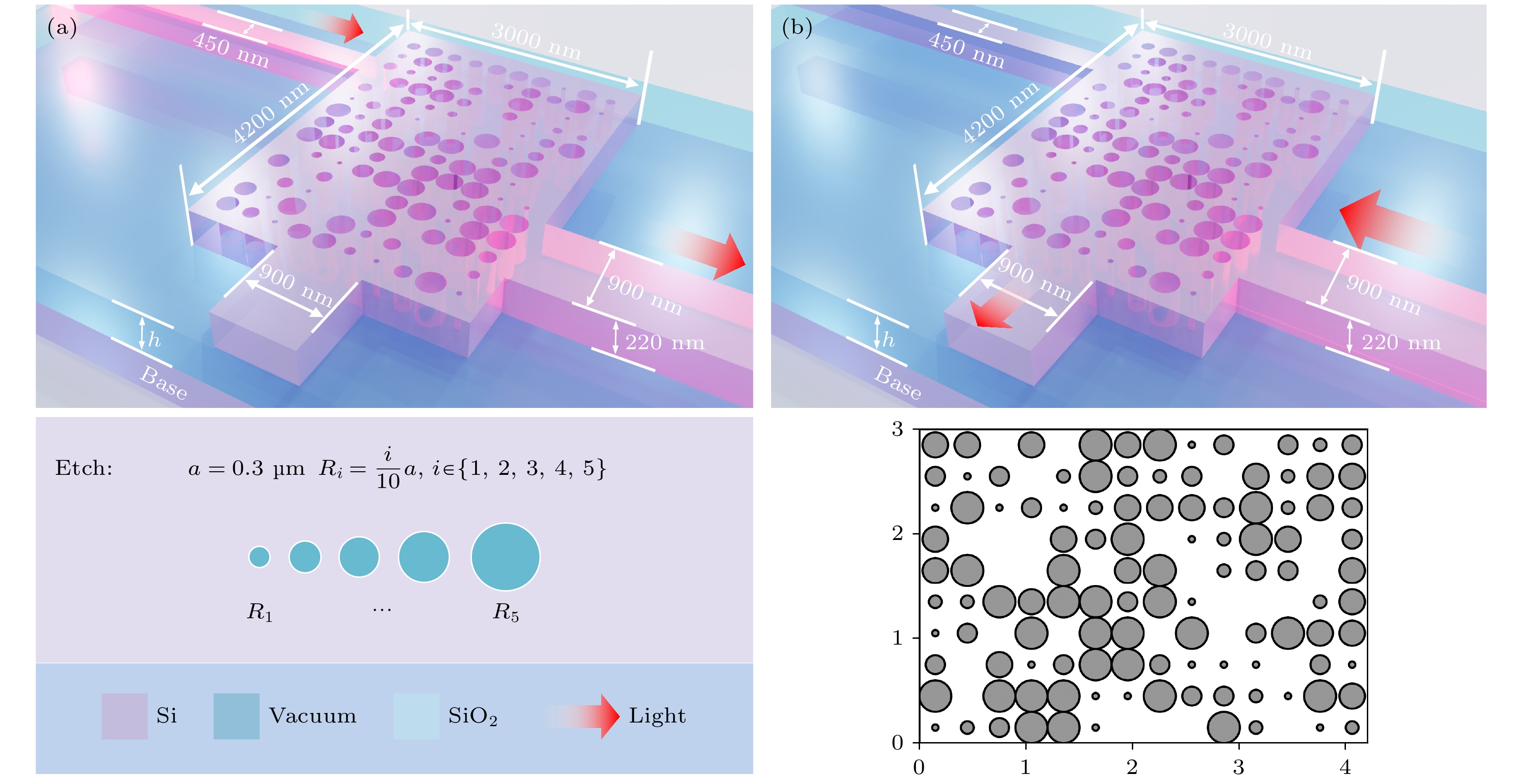
图 1 隔离器结构示意图 (a)正向导通示意图, 下方是优化过程中可供选择的5种不同的圆孔孔径参数; (b)反向通光示意图. 下方是1550 nm的TM模式光源经过1500次迭代后最优价值函数对应的隔离器结构分布图
Figure 1. Isolator structure diagram: (a) Schematic diagram of the forward guide, below which are the five different round hole aperture parameters that can be selected during the optimization process; (b) reverse light passing diagram. The structure below is the distribution diagram of the isolator structure corresponding to the optimal value function of the 1550 nm TM mode light source after 1500 iterations.
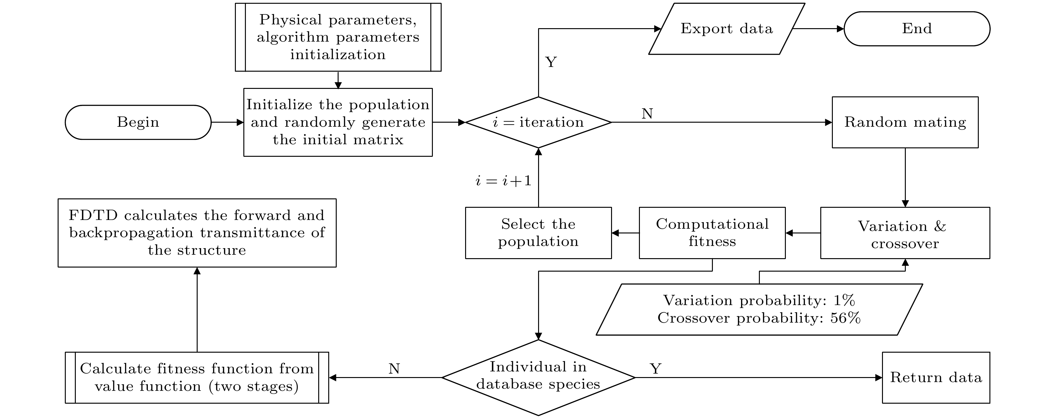
图 2 遗传算法的流程图
Figure 2. Flow chart of genetic algorithm
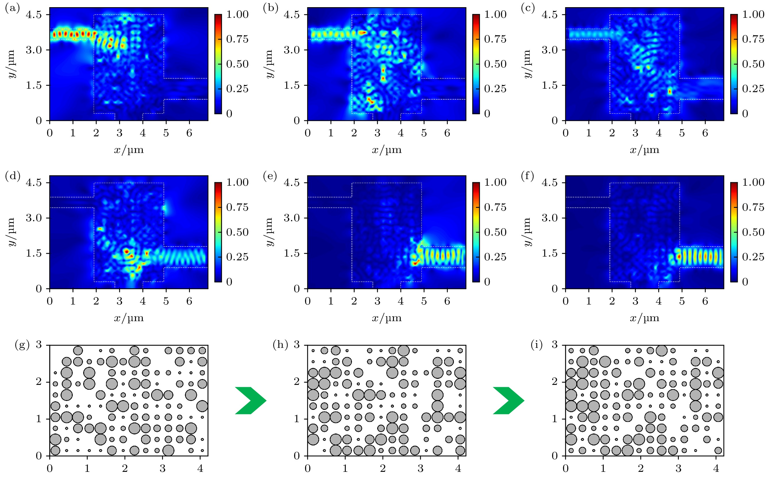
图 3 遗传算法的最优结构在正向、反向传播时光场模场分布和对应的结构分布图 (a), (d), (g)迭代1次; (b), (e), (h)迭代11次; (c), (f), (i) 迭代201次
Figure 3. Optimal structure of genetic algorithm in the forward and backward propagation of power distribution and the corresponding structure distribution diagram: (a), (d), (g) Iteration 1 times; (b), (e), (h) 11 iterations; (c), (f), (i) 201 iterations.
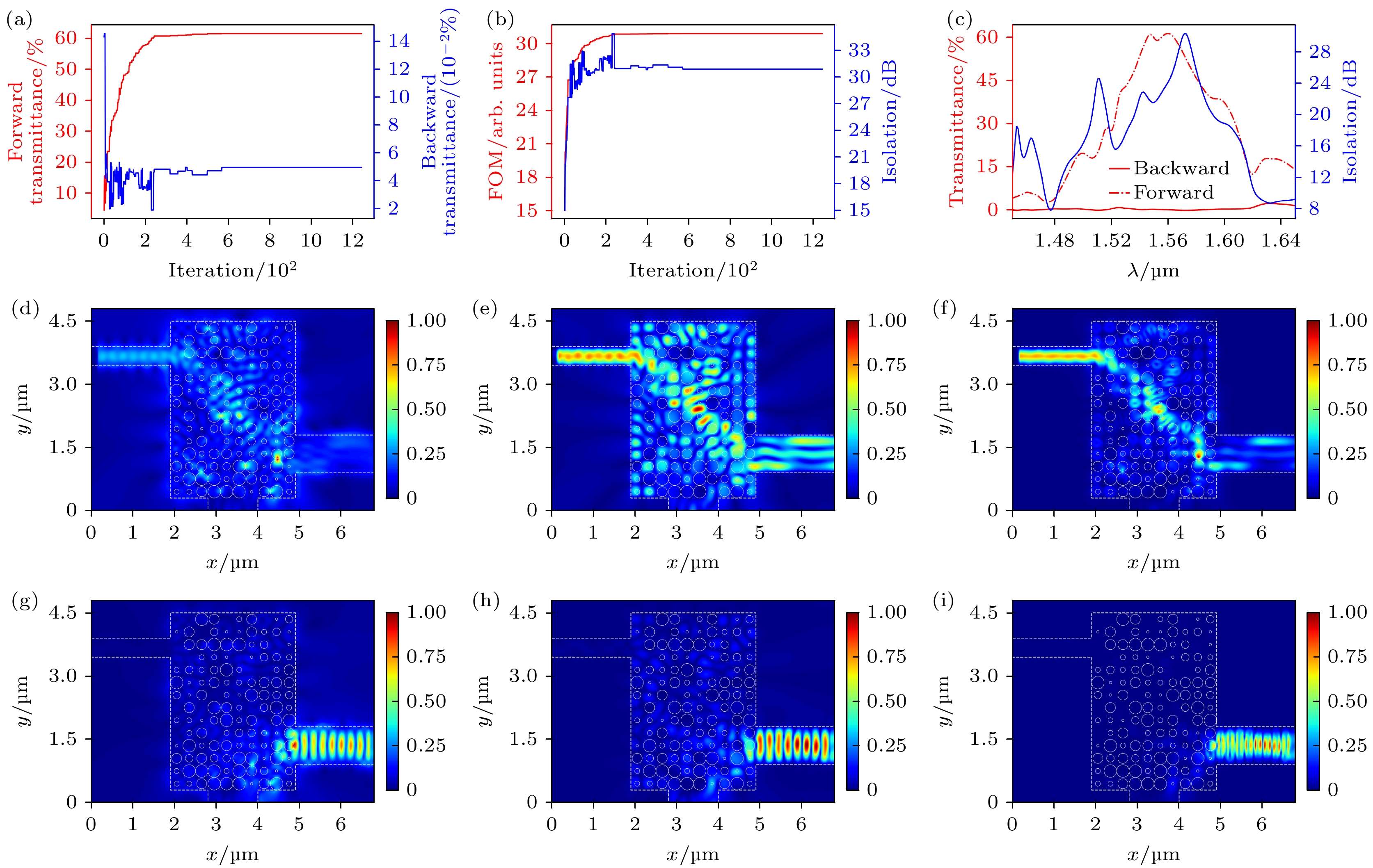
图 4 将光源设置为1550 nm TE偏振的优化结果 (a) 透射率随着迭代次数的变化曲线; (b) 价值函数和隔离度随着算法的迭代的变化曲线; (c) 不同波长通过结构的透射率分布曲线; (d), (g) 正向、反向通光时的电场模场分布图; (e), (h) 正向、反向通光时的磁场分布图; (f), (i) 正向、反向通光时的光场模场分布图
Figure 4. Optimization results of setting the light source to 1550 nm TE polarization: (a) Transmittance with the number of iterations; (b) variation curve of the value function and isolation degree with the iteration of the algorithm; (c) transmittance distribution curves of different wavelengths through the structure; (d), (g) mode field distribution of the electric field when the light is transmitted in the forward and reverse directions; (e), (h) magnetic field distribution in forward and reverse transmission; (f), (i) power distribution diagram for forward and reverse transmission
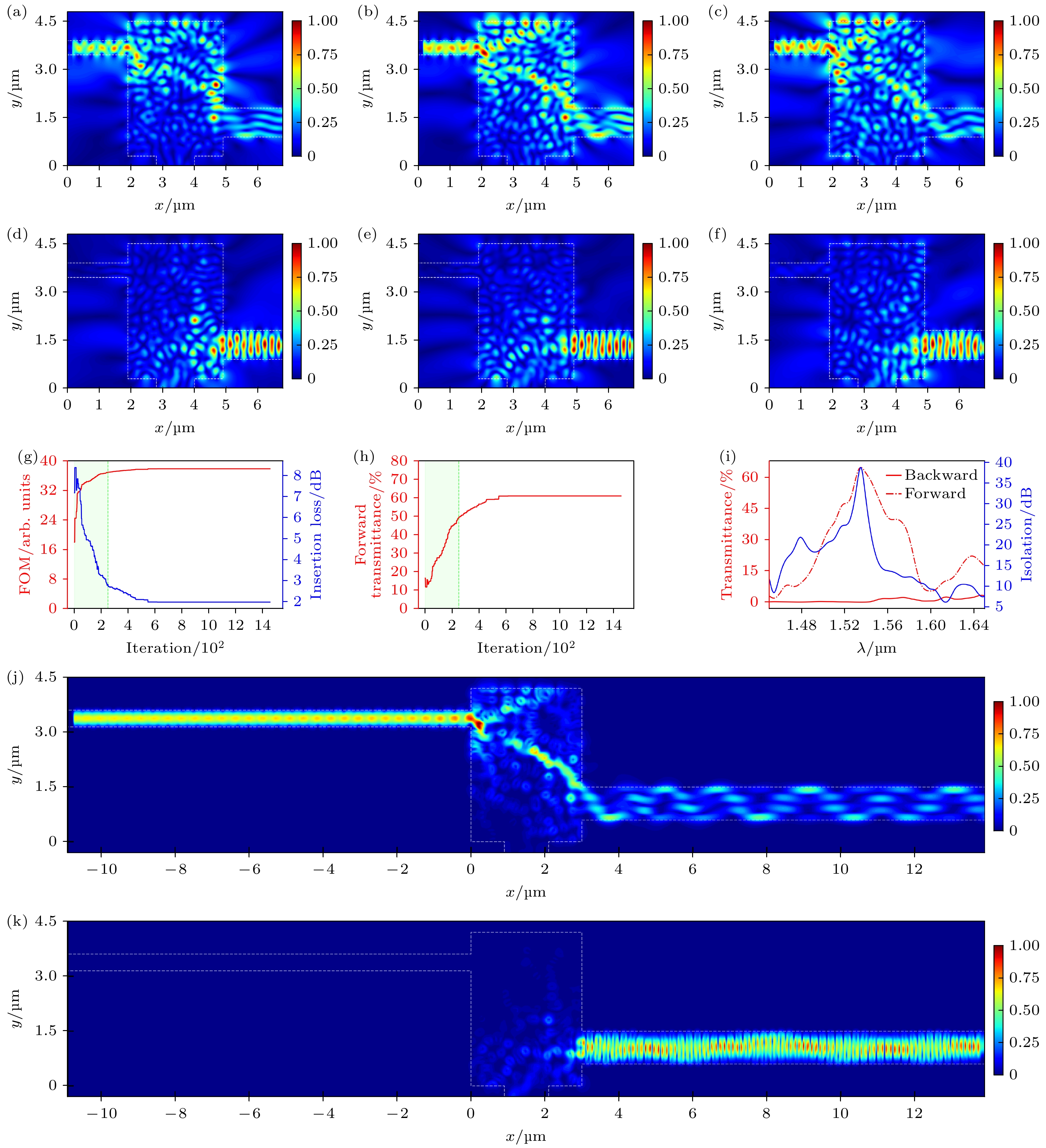
图 5 TM偏振的优化结果 (a), (d) 1535 nm处的光场模场分布图; (b), (e) 1555 nm处的光场模场分布图; (c), (f) 1575 nm处的光场模场分布图; (g)隔离度、插入损耗的变化曲线; (h)透射率的变化曲线; (i)不同波长的光源通过结构的透射率和隔离度分布曲线; (j), (k) 1550nm TM光源正向和反向通过结构的光场模场分布图
Figure 5. Optimization results of TM polarization: (a), (d) Optical power distribution at 1535 nm; (b), (e) optical power distribution at 1555 nm; (c), (f) optical power distribution at 1575 nm; (g) variation curves of isolation and insertion loss; (h) variation curves of transmittance; (i) transmittance curves and isolation distribution curves of different wavelengths of the light source passing through the structure; (j), (k) mode-field distribution of the light field of a 1550 nm TM light source passing through the structure in the forward and reverse directions.
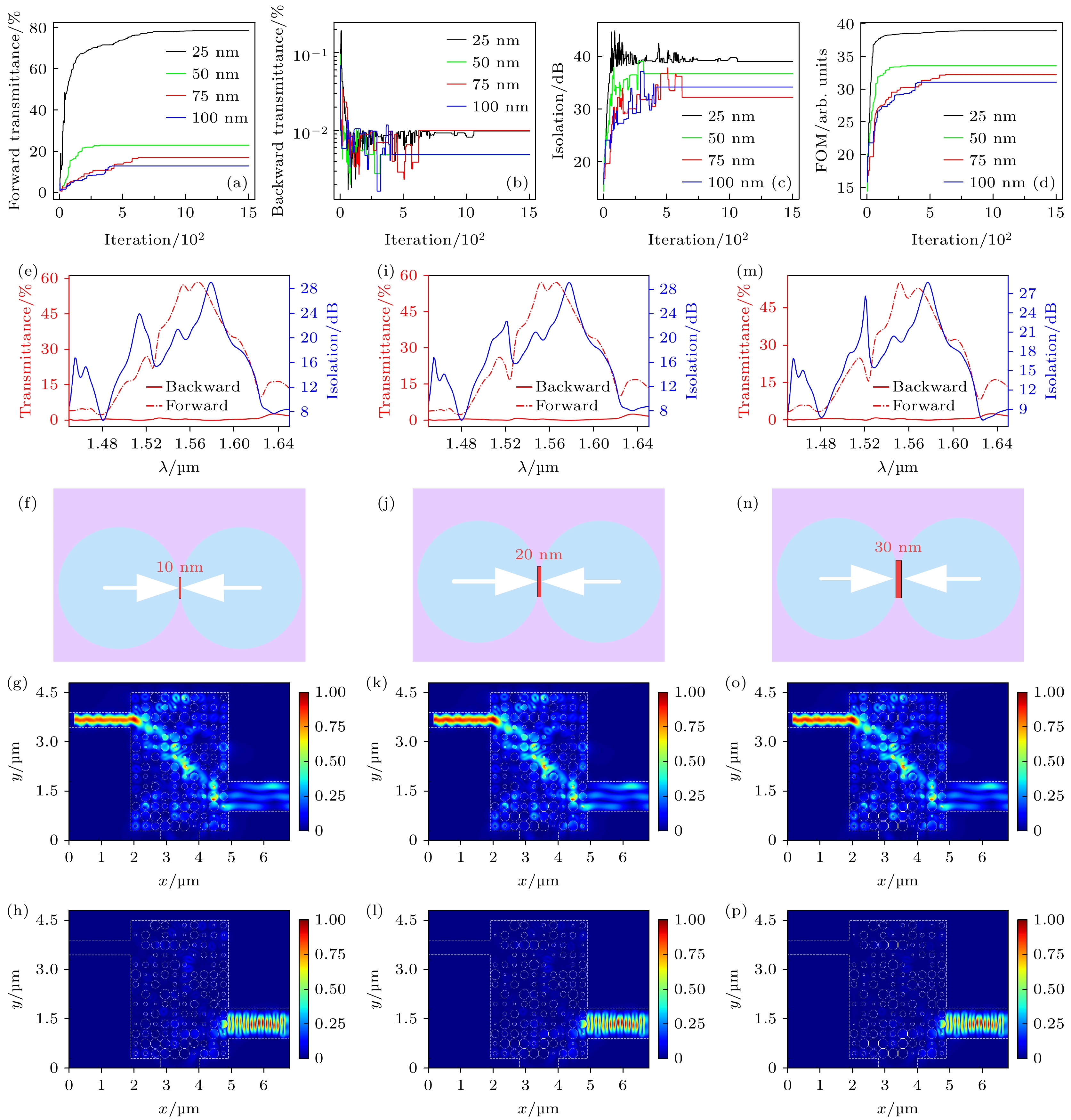
图 6 四种特征尺寸随迭代次数的变化曲线和刻蚀穿透间距离 (a) 正向透射率; (b) 反向透射率; (c) 隔离度; (d) 价值函数; (e)—(h) 刻蚀10 nm孔间距得到的透射率曲线、示意图和光场模场分布图; (i)—(l) 刻蚀20 nm得到的结果; (m)—(p) 刻蚀30 nm得到的结果
Figure 6. Variation curves of the four feature sizes with the number of iterations and the distance between the etched penetrations: (a) Forward transmittance; (b) reverse transmittance; (c) isolation; (d) FOM function; (e)–(h) transmittance curves, schematic and power distribution plots obtained by etching 10 nm pore spacing; (i)–(l) results obtained by etching 20 nm; (m)–(p) results obtained by etching 30 nm.
-
[1] Yu M, Cheng R, Reimer C, He L, Luke K, Puma E, Shao L, Shams-Ansari A, Ren X, Grant H R, Johansson L, Zhang M, Lončar M 2023 Nat. Photonics 17 666
Google Scholar
[2] Huang D, Pintus P, Shoji Y, Morton P, Mizumoto T, Bowers J E 2017 Opt. Lett. 42 23
Google Scholar
[3] Pintus P, Huang D, Zhang C, Shoji Y, Mizumoto T, Bowers J E 2017 J. Lightwave Technol. 35 1429
Google Scholar
[4] Bi L, Hu J, Jiang P, Kim D H, Dionne G F, Kimerling L C, Ross C 2011 Nat. Photonics 5 758
Google Scholar
[5] Onbasli M C, Beran L, Zahradník M, Kučera M, Antoš R, Mistrík J, Dionne G F, Veis M, Ross C A 2016 Sci. Rep. 6 23640
Google Scholar
[6] White A D, Ahn G H, Gasse K V, Yang K Y, Chang L, Bowers J E, Vučković J 2023 Nat. Photonics 17 143
Google Scholar
[7] Abdelsalam K, Li T, Khurgin J B, Fathpour S 2020 Optica 7 209
Google Scholar
[8] Dostart N, Gevorgyan H, Onural D, Popović M A 2021 Opt. Lett. 46 460
Google Scholar
[9] Lira H, Yu Z, Fan S, Lipson M 2012 Phys. Rev. Lett. 109 033901
Google Scholar
[10] Herrmann J F, Ansari V, Wang J, Witmer J D, Fan S, Safavi-Naeini A H 2022 Nat. Photonics 16 603
Google Scholar
[11] Yu Z, Fan S 2009 Nat. Photonics 3 91
Google Scholar
[12] Kang M S, Butsch A, Russell P S J 2011 Nat. Photonics 5 549
Google Scholar
[13] Wang C, Zhou C Z, Li Z Y 2011 Opt. Express 19 26948
Google Scholar
[14] Wang C, Zhong X L, Li Z Y 2012 Sci. Rep. 2 674
Google Scholar
[15] Mizumoto T, Shoji Y 2020 Optical Fiber Communication Conference (OFC) 2020 San Diego, California, United States, March 8–12, 2020 pT3B.1
[16] Karki D, Stenger V, Pollick A, Levy M 2020 J. Lightwave Technol. 38 827
Google Scholar
[17] Tian H, Liu J, Siddharth A, Wang R N, Blésin T, He J, Kippenberg T J, Bhave S A 2021 Nat. Photonics 15 828
Google Scholar
[18] Seldowitz M A, Allebach J P, Sweeney D W 1987 Appl. Opt. 26 2788
Google Scholar
[19] Yuan H, Wu J, Zhang J, Pu X, Zhang Z, Yu Y, Yang J 2022 Nanomaterials 12 669
Google Scholar
[20] Peng Z, Feng J, Yuan H, et al. 2022 Nanomaterials 12 1121
Google Scholar
[21] Lalau-Keraly C M, Bhargava S, Miller O D, Yablonovitch E 2013 Opt. Express 21 21693
Google Scholar
[22] Keraly C L, Bhargava S, Ganapati V, et al. 2014 CLEO: Science and Innovations 2014 San Jose, California, United States, June 8–13, 2014 pSTu2 M.6
[23] Liao J, Tian Y, Yang Z, Xu H, Tang C, Wang Y, Zhang X, Kang Z 2024 Chin. Opt. Lett. 22 011302
Google Scholar
[24] Wang Z, Feng J, Li H, Zhang Y, Wu Y, Hu Y, Wu J, Yang J 2023 Nanomaterials 13 2516
Google Scholar
[25] Piggott A Y, Lu J, Lagoudakis K G, Petykiewicz J, Babinec T M, Vučković J 2015 Nat. Photonics 9 374
Google Scholar
[26] Nanda A, Kues M, Calà Lesina A 2024 Opt. Lett. 49 1125
Google Scholar
[27] Vercruysse D, Sapra N V, Su L, Trivedi R, Vučković J 2019 Sci. Rep. 9 8999
Google Scholar
[28] Cao J, Zhao Z, Sun H, Yang Y, Deng Y, Cao P 2023 J. Phys.: Conf. Ser. 2464 012019
Google Scholar
[29] Mak J C, Sideris C, Jeong J, Hajimiri A, Poon J K 2016 Opt. Lett. 41 3868
Google Scholar
[30] Yao R, Li H, Zhang B, Chen W, Wang P, Dai S, Liu Y, Li J, Li Y, Fu Q, Dai T, Yu H, Yang J, Pavesi L 2021 J. Lightwave Technol. 39 6253
Google Scholar
[31] Lee I, Kim C, Ju K, Jun G, Yoon G 2023 Appl. Opt. 62 8994
Google Scholar
[32] Jia W, Jiang L, Li X 2010 Opt. Commun. 283 1537
Google Scholar
[33] Yu Z, Cui H, Sun X 2017 Opt. Lett. 42 3093
Google Scholar
[34] Mirzaei A, Miroshnichenko A E, Shadrivov I V, Kivshar Y S 2014 Appl. Phys. Lett. 105 011109
Google Scholar
[35] Wang Z, Peng Z, Zhang Y, Wu Y, Hu Y, Wu J, Yang J 2023 Opt. Express 31 15904
Google Scholar
[36] Peng Z, Feng J, Du T, Cheng W, Wang Y, Zang S, Cheng H, Ren X, Shuai Y, Liu H, Wu J, Yang J 2022 Opt. Express 30 27366
Google Scholar
[37] Cakirlar C, Galderisi G, Beyer C, Simon M, Mikolajick T, Trommer J 2022 2022 IEEE 22nd International Conference on Nanotechnology (NANO) Palma de Mallorca, Spain, July 4–8, 2022 pp207–210
[38] Saifullah M, Subramanian K, Tapley E, Kang D J, Welland M, Butler M 2003 Nano Lett. 3 1587
Google Scholar
[39] Wang K, Ren X, Chang W, Lu L, Liu D, Zhang M 2020 Photonics Res. 8 528
Google Scholar


 DownLoad:


Catalog
Metrics
- Abstract views: 1390
- PDF Downloads: 72
- Cited By: 0
