-
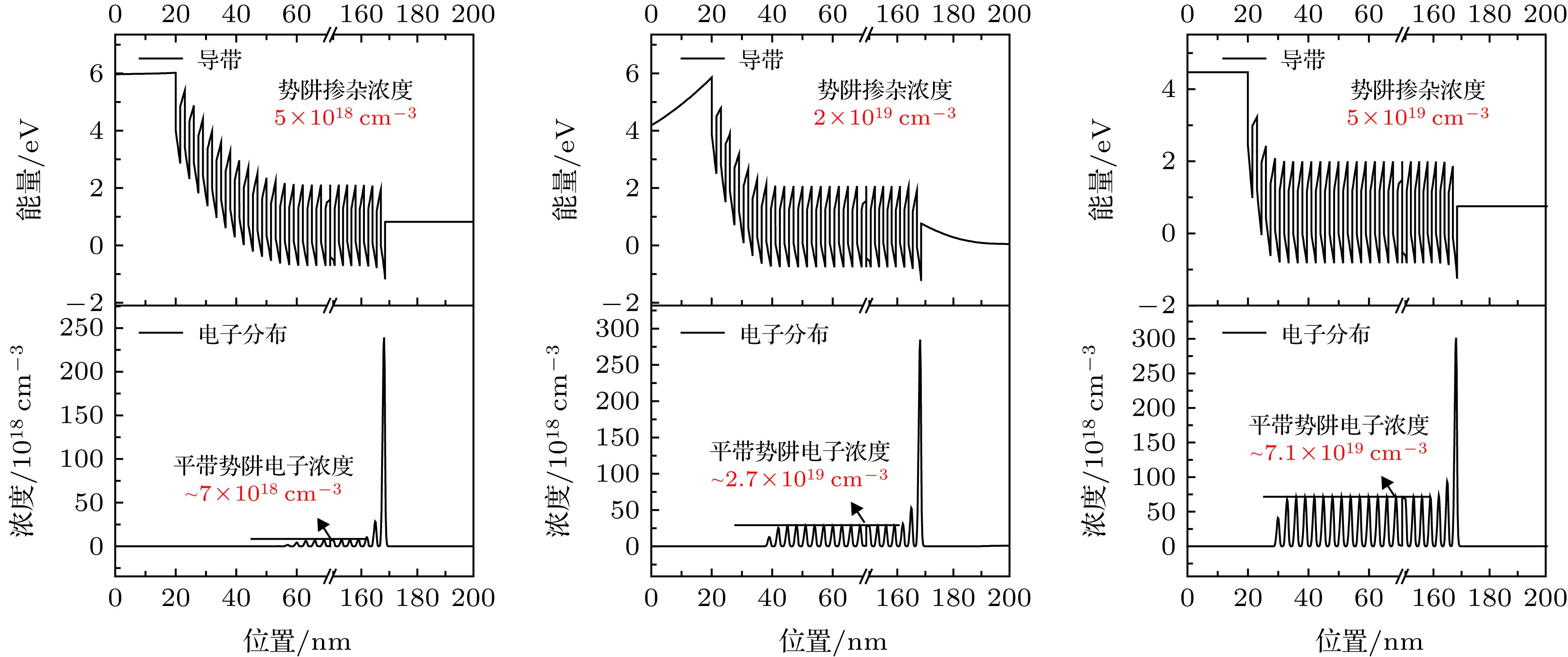
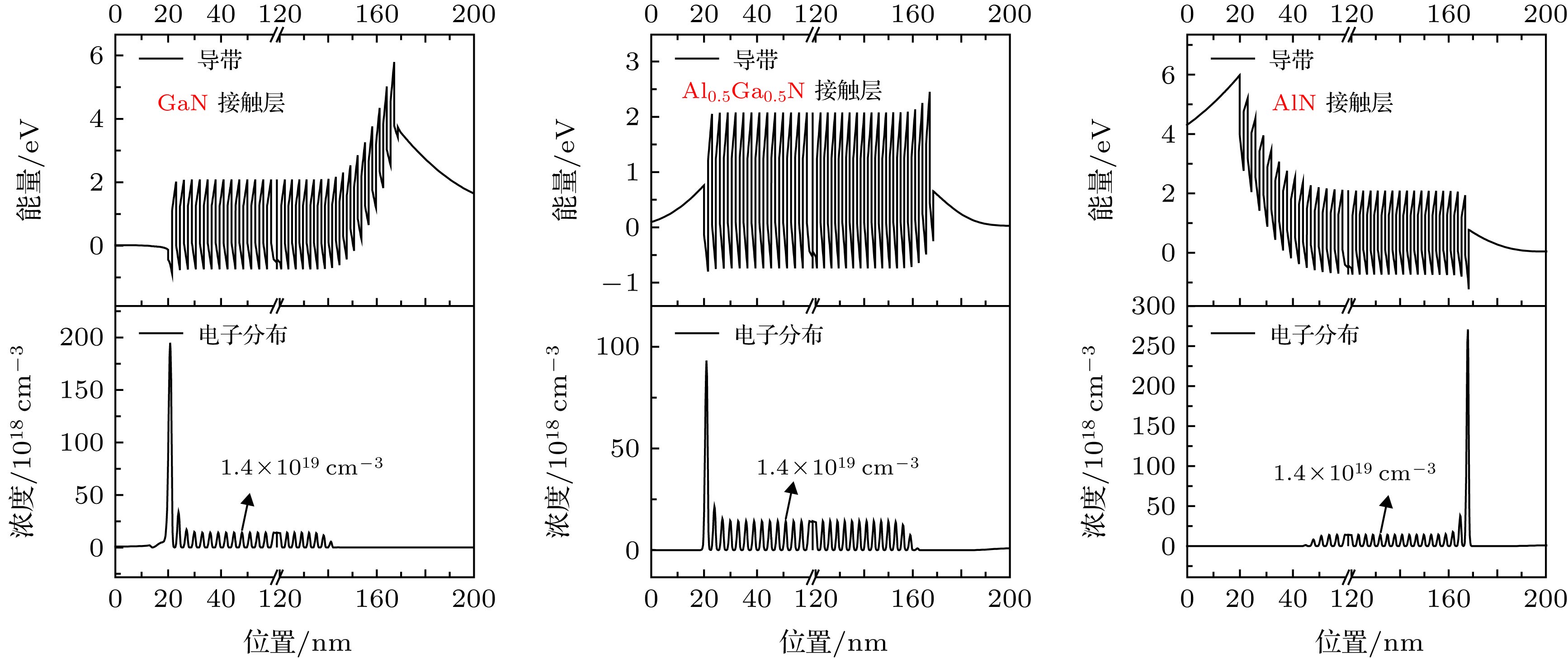
氮化物子带跃迁探测器具备在近红外通讯波段高速工作和在太赫兹波段室温工作的潜力, 但材料强的极化作用容易造成器件效率降低. 本文分别针对工作于上述波段的典型器件, 理论分析了材料结构参数对器件能带结构、载流子浓度分布、极化效应以及光生载流子隧穿的影响. 近红外波段器件以光伏型器件结构为基础, 研究发现增加量子势阱的周期数、增大势阱掺杂浓度、以及保持接触层材料晶格常数与超晶格有源区平均晶格常数相同, 有助于增加基态能级上被载流子填充的量子势阱数, 从而增强器件的吸收效率. 太赫兹波段器件以双台阶器件结构为基础, 研究表明器件设计时即使任意调节势阱层和势垒层厚度, 也不会改变影响光生载流子传输的势垒层极化电场分布. 同时, 降低台阶势垒层铝组分和适当增加其厚度可以提高光生载流子隧穿通过台阶势垒层的效率. 本文仿真结果对于设计优化的氮化物子带跃迁探测器材料结构、提升器件性能具有指导意义.
The photodetection potential applications of III-nitride semiconductor are not only restricted in the ultraviolet range, but also extended to the infrared and even terahertz wave range through intersubband transition (ISBT) process between quantum-confined electronic states. The large conduction band offset (~1.75 eV for GaN/AlN heterostructures) and the strong electron-phonon interaction in these materials enable the III-nitride ISBT photodetectors to operate with ultrahigh speed for near-infrared telecommunication applications. Furthermore, due to the large energy of longitudinal optical phonons of nitride materials (~92 meV for GaN), the corresponding ISBT photodetectors are demonstrated as a promising candidate for operating in a specific terahertz (THz) range (5-12 THz) at high temperature, which is fundamentally in accessible to As-based devices. One of the major difficulties in realizing high performance III-nitride ISBT photodetectors is the existence of undesired polarization field inherited from conventional c-axis nitrides, which greatly makes the design complicated. In this paper, we theoretically study the influences of critical material structure parameters on the band structure, electron distribution, polarization field intensity, and tunneling effect based on near-infrared photovoltaic photodetectors and terahertz double-step photodetectors. III-nitride ISBT photodetectors operating in near-infrared are designed to be able to suppress the internal electric field in the active region, so that as many quantum wells as possible can be populated by electrons to enhance the absorption efficiency. It is found that with the increase of well periods and well doping concentration, a weaker average polarization field is observed, and as a result more wells will be populated with electrons. In addition, keeping the lattice constant of the contact layer material the same as the average lattice constant of the active region is beneficial to making more quantum wells effectively populated with electrons. On the other hand, the devices operating in a terahertz range require a more accurate design of energy band than the near-infrared ones due to its rather small energy interval. The design difficulties lie in how to ensure both the efficient absorption of photons and the following transportation of photo-excited electrons in the presence of polarization-induced field. The simulation results indicate that the polarization field in an active region is sensitive to the aluminum mole composition of barrier layer, the thickness of step well and step barrier layers, while even if the thickness of well and barrier layers change, the polarization field in barrier layer will stay the same. Moreover, reducing the aluminum mole composition of step barrier layer or appropriately increasing its thickness will be helpful in enhancing the photo-excited electrons tunneling. The above knowledge is beneficial to the optimal design of III-nitride ISBT photodetectors with high efficiency. -
Keywords:
- nitrides /
- intersubband transition /
- photodetector /
- quantum well
[1] Preethi P, Bruce H, Shouleh N, Douglas L B, Kees K, Edoardo C 2018 Sensors 18 449
 Google Scholar
[2] 雷双瑛, 沈波, 张国义 2008 57 2386
 Google Scholar
Lei S Y, Shen B, Zhang G Y 2008 Acta Phys. Sin. 57 2386
 Google Scholar
[3] Beeler M, Trichas E, Monroy E 2013 Semicond. Sci. Technol. 28 074022
 Google Scholar
[4] Kandaswamy P K, Guillot F, Bellet-Amalric E, Monroy E, Nevou L, Tchernycheva M, Michon A, Julien F H, Baumann E, Giorgetta F R, Hofstetter D, Remmele T, Albrecht M, Birner S, Dang L S 2008 J. Appl. Phys. 104 093501
 Google Scholar
[5] Vardi A, Bahir G, Guillot F, Bougerol C, Monroy E, Schacham S E, Tchernycheva M, Julien F H 2008 Appl. Phys. Lett. 92 011112
 Google Scholar
[6] Lähnemann J, Ajay A, Den Hertog M I, Monroy E 2017 Nano Lett. 17 6954
 Google Scholar
[7] Durmaz H, Nothern D, Brummer G, Moustakas T D, Paiella R 2016 Appl. Phys. Lett. 108 201102
 Google Scholar
[8] Beeler M, Bougerol C, Bellet-Amalric E, Monroy E 2013 Appl. Phys. Lett. 103 091108
 Google Scholar
[9] Rong X, Wang X Q, Chen G, Zheng X T, Wang P, Xu F J, Qin Z X, Tang N, Chen Y H, Sang L W, Sumiya M, Ge W K, Shen B 2015 Sci. Rep. 5 14386
 Google Scholar
[10] Tchernycheva M, Nevou L, Doyennette L, Julien F H, Warde E, Guillot F, Monroy E, Bellet-Amalric E, Remmele T, Albrecht M 2006 Phys. Rev. B 73 125347
 Google Scholar
[11] Iizuka N, Kaneko K, Suzuki N 2005 Opt. Express 13 3835
 Google Scholar
[12] Kang J B, Li M, Li Q, Wang W P, Chen F L, Zhang J 2017 International Conference on Numerical Simulation of Optoelectronic Devices Copenhagen, Danmark, July 24–28, 2017 p215
[13] Machhadani H, Kandaswamy P, Sakr S, Vardi A, Wirtmüller A, Nevou L, Guillot F, Pozzovivo G, Tchernycheva M, Lupu A, Vivien L, Croza P, Warde E, Bougerol C, Schacham S, Strasser G, Bahir G, Monroy E, Julien F H 2009 New J. Phys. 11 125023
 Google Scholar
[14] Machhadani H, Tchernycheva M, Sakr S, Rigutti L, Colombelli R, Warde E, Mietze C, As D J, Julien F H 2011 Phys. Rev. B 83 075313
 Google Scholar
[15] Wu F, Tian W, Yan W Y, Zhang J, Sun S C, Dai J N, Fang Y Y, Wu Z H, Chen C Q 2013 J. Appl. Phys. 113 154505
 Google Scholar
[16] Kang J B, Li Q, Li M, Wang W P, Chen F L, Zhang J 2018 International Conference on Numerical Simulation of Optoelectronic Devices Hong Kong, China, November 5–9, 2018 p111
[17] Sudradjat F F, Zhang W, Woodward J, Durmaz H, Moustakas T D, Paiella R 2012 Appl. Phys. Lett. 100 241113
 Google Scholar
[18] Liu D F, Cheng Y, He J F 2015 Superlattice Microst. 86 313
 Google Scholar
[19] Fu H Q, Lu Z J, Huang X Q, Chen H, Zhao Y J 2016 J. Appl. Phys. 119 174502
 Google Scholar
[20] Cen L B, Shen B, Qin Z X, Zhang G Y 2008 J. Appl. Phys. 104 063114
 Google Scholar
[21] Birner S, Schindler C, Greck P, Sabathil M, Vogl P 2009 J. Comput. Electron. 8 267
 Google Scholar
[22] Giorgetta F R, Baumann E, Guillot F, Monroy E, Hofstetter D 2007 Electron. Lett. 43 1
 Google Scholar
[23] Hofstetter D, Baumann E, Giorgetta F R, Guillot F, Leconte S, Monroy E 2007 Appl. Phys. Lett. 91 131115
 Google Scholar
[24] Kandaswamy P K, Machhadani H, Kotsar Y, Sakr S, Das A, Tchernycheva M, Rapenne L, Sarigiannidou E, Julien F H, Monroy E 2010 Appl. Phys. Lett. 96 141903
 Google Scholar
-
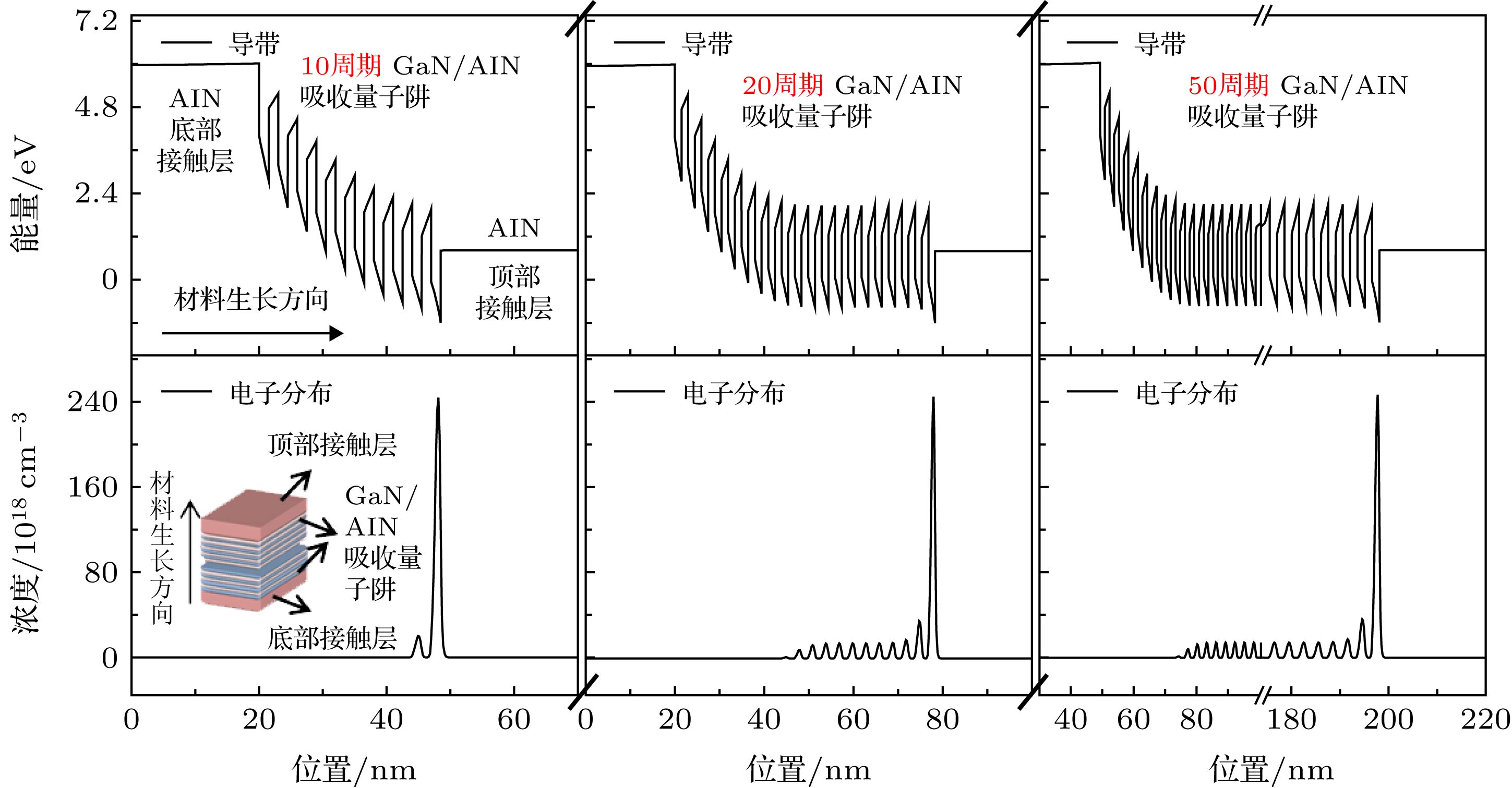
图 1 典型光伏型GaN/AlN子带跃迁探测器量子阱周期数分别为10, 20, 50情况下的导带结构和电子浓度分布, 左下侧的插图为器件材料结构示意图
Fig. 1. Conduction band profile and electron distribution for typical photovoltaic nitride intersubband photodetectors, with ten periods, twenty periods and fifty periods of GaN/AlN quantum wells, respectively. The inset shows the schematic image of the sample structure.
图 6 双台阶结构器件中势垒层极化电场随各层材料厚度变化的关系(右侧纵坐标), 以及为了保持势垒层中极化电场始终为零, 势垒层Al组分随厚度的变化关系(左侧纵坐标)
Fig. 6. The influence of each layer thickness on the barrier layer polarization fields (right ordinates) and the change of Al mole composition of barrier under the condition that the polarization field in barrier layer is kept at zero (left ordinates) for double-step devices.
-
[1] Preethi P, Bruce H, Shouleh N, Douglas L B, Kees K, Edoardo C 2018 Sensors 18 449
 Google Scholar
[2] 雷双瑛, 沈波, 张国义 2008 57 2386
 Google Scholar
Lei S Y, Shen B, Zhang G Y 2008 Acta Phys. Sin. 57 2386
 Google Scholar
[3] Beeler M, Trichas E, Monroy E 2013 Semicond. Sci. Technol. 28 074022
 Google Scholar
[4] Kandaswamy P K, Guillot F, Bellet-Amalric E, Monroy E, Nevou L, Tchernycheva M, Michon A, Julien F H, Baumann E, Giorgetta F R, Hofstetter D, Remmele T, Albrecht M, Birner S, Dang L S 2008 J. Appl. Phys. 104 093501
 Google Scholar
[5] Vardi A, Bahir G, Guillot F, Bougerol C, Monroy E, Schacham S E, Tchernycheva M, Julien F H 2008 Appl. Phys. Lett. 92 011112
 Google Scholar
[6] Lähnemann J, Ajay A, Den Hertog M I, Monroy E 2017 Nano Lett. 17 6954
 Google Scholar
[7] Durmaz H, Nothern D, Brummer G, Moustakas T D, Paiella R 2016 Appl. Phys. Lett. 108 201102
 Google Scholar
[8] Beeler M, Bougerol C, Bellet-Amalric E, Monroy E 2013 Appl. Phys. Lett. 103 091108
 Google Scholar
[9] Rong X, Wang X Q, Chen G, Zheng X T, Wang P, Xu F J, Qin Z X, Tang N, Chen Y H, Sang L W, Sumiya M, Ge W K, Shen B 2015 Sci. Rep. 5 14386
 Google Scholar
[10] Tchernycheva M, Nevou L, Doyennette L, Julien F H, Warde E, Guillot F, Monroy E, Bellet-Amalric E, Remmele T, Albrecht M 2006 Phys. Rev. B 73 125347
 Google Scholar
[11] Iizuka N, Kaneko K, Suzuki N 2005 Opt. Express 13 3835
 Google Scholar
[12] Kang J B, Li M, Li Q, Wang W P, Chen F L, Zhang J 2017 International Conference on Numerical Simulation of Optoelectronic Devices Copenhagen, Danmark, July 24–28, 2017 p215
[13] Machhadani H, Kandaswamy P, Sakr S, Vardi A, Wirtmüller A, Nevou L, Guillot F, Pozzovivo G, Tchernycheva M, Lupu A, Vivien L, Croza P, Warde E, Bougerol C, Schacham S, Strasser G, Bahir G, Monroy E, Julien F H 2009 New J. Phys. 11 125023
 Google Scholar
[14] Machhadani H, Tchernycheva M, Sakr S, Rigutti L, Colombelli R, Warde E, Mietze C, As D J, Julien F H 2011 Phys. Rev. B 83 075313
 Google Scholar
[15] Wu F, Tian W, Yan W Y, Zhang J, Sun S C, Dai J N, Fang Y Y, Wu Z H, Chen C Q 2013 J. Appl. Phys. 113 154505
 Google Scholar
[16] Kang J B, Li Q, Li M, Wang W P, Chen F L, Zhang J 2018 International Conference on Numerical Simulation of Optoelectronic Devices Hong Kong, China, November 5–9, 2018 p111
[17] Sudradjat F F, Zhang W, Woodward J, Durmaz H, Moustakas T D, Paiella R 2012 Appl. Phys. Lett. 100 241113
 Google Scholar
[18] Liu D F, Cheng Y, He J F 2015 Superlattice Microst. 86 313
 Google Scholar
[19] Fu H Q, Lu Z J, Huang X Q, Chen H, Zhao Y J 2016 J. Appl. Phys. 119 174502
 Google Scholar
[20] Cen L B, Shen B, Qin Z X, Zhang G Y 2008 J. Appl. Phys. 104 063114
 Google Scholar
[21] Birner S, Schindler C, Greck P, Sabathil M, Vogl P 2009 J. Comput. Electron. 8 267
 Google Scholar
[22] Giorgetta F R, Baumann E, Guillot F, Monroy E, Hofstetter D 2007 Electron. Lett. 43 1
 Google Scholar
[23] Hofstetter D, Baumann E, Giorgetta F R, Guillot F, Leconte S, Monroy E 2007 Appl. Phys. Lett. 91 131115
 Google Scholar
[24] Kandaswamy P K, Machhadani H, Kotsar Y, Sakr S, Das A, Tchernycheva M, Rapenne L, Sarigiannidou E, Julien F H, Monroy E 2010 Appl. Phys. Lett. 96 141903
 Google Scholar
计量
- 文章访问数: 8771
- PDF下载量: 70
- 被引次数: 0


 下载:
下载:


