


-
聚合物衬底克服了刚性平面衬底在空间形变场景下的局限, 并能结合光刻技术制备复杂三维异形空间结构. 光热冲镊技术实现了固体界面上对微纳物体的捕获和操控, 将该技术应用在聚合物衬底上可开发新的应用场景需求. 本文以常用的聚甲基丙烯酸甲酯和负性光刻胶作为聚合物衬底, 通过溶胶-凝胶法在其上制备SiO2纳米薄膜, 能有效减轻光热冲击效应引起的热损伤, 从而实现微纳物体的激光捕获及操控. 实验表明, 在常用激光操控功率条件下, 当SiO2纳米薄膜厚度大于110 nm时, 能够有效防止聚合物衬底因光热效应引起软化、膨胀和表面破坏. 理论计算也表明, 纳米薄膜能至少使聚合物表面温度降低111 ℃, 并使其产生最高温度的时间滞后13.2 ns. 本文使用的纳米薄膜制备技术具有常温、大面积、低粗糙度且厚度均一的优点, 能普遍适用于柔性聚合物衬底以及异形结构. 本实验结果拓展了激光捕获物体的环境媒介, 为其在微纳操控、微纳米机器人和微纳光机电器件等领域的应用提供新的可能性.
Polymer substrates break through the limitations of rigid planar substrates in spatial deformation scenarios and can be combined with photolithography to fabricate complex, three-dimensional irregular polymer structures. Photothermal-shock tweezer is a laser trapping technique based on the photothermal shock effect. Photothermal-shock tweezer uses pulsed laser induced transient photothermal shock to generate micro-newton-scale thermomechanical strain gradient force, enabling the trapping and manipulation of micro/nano-objects at solid interfaces. Integrating this technique with polymer substrates can meet the demands of new application scenarios. In this work, commonly employed polymethyl methacrylate (PMMA) and negative photoresist (SU-8) are used as polymer substrates, on which SiO2 nanofilms are prepared using the sol-gel method. This method effectively mitigates thermal damage caused by photothermal shock effects, enabling laser trapping and manipulation of micro/nano-objects. The SiO2 nanofilms, characterized by low thermal conductivity, effectively inhibit heat transfer. The nanofilm fabrication technique utilized in this study enables the synthesizing of large-area SiO2 nanofilms with large-area coverage, low surface roughness (Rq ~ 320 pm) and uniform thickness, making them broadly applicable to flexible polymer substrates and irregular structures. Direct contact between the polymer layer and micro/nano-objects during manipulating the photothermal shock tweezer can induce irreversible substrate degradation due to transient photothermal shock effects. Experimental results demonstrate that depositing an SiO2 nanofilm thicker than 110 nm on the polymer substrate can significantly enhance thermal insulation and protection, effectively mitigating laser-induced damage under typical optical manipulation conditions. Additionally, by analyzing the temperature field distribution of the gold nanosheet, PMMA substrate, and SiO2 nanofilm during a single photothermal shock trapping of a gold nanosheet, it is found that the SiO2 nanofilm can reduce the PMMA surface temperature by at least 111 ℃ and delay the time for PMMA to reach its peak temperature by 13.2 ns compared with the the gold nanosheet. The experimental results expand the environmental medium for laser trapping of objects, providing new possibilities for applications in micro/nano-manipulation, micro/nanorobotics, and micro/nano-optoelectronic devices. 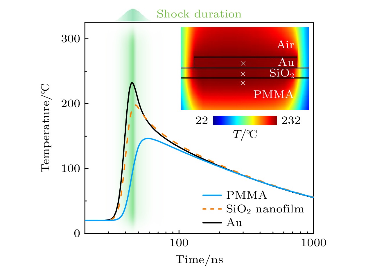
-
Keywords:
- laser trapping /
- polymer surface /
- sol-gel method /
- photothermal-shock tweezer
[1] Li N, Zhu X M, Li W Q, Fu Z H, Hu M Z, Hu H Z 2019 Front. Inform. Technol. Electron. Eng. 20 655
 Google Scholar
[2] 汪涵聪, 李志鹏 2019 68 144101
Google Scholar
Wang H C, Li Z P 2019 Acta Phys. Sin. 68 144101
Google Scholar
[3] 韩翔, 陈鑫麟, 熊威, 邝腾芳, 陈志洁, 彭妙, 肖光宗, 杨开勇, 罗晖 2021 中国激光 48 0401011
Google Scholar
Han X, Chen X L, Xiong W, Kuang T F, Chen Z H, Peng M, Xiao G Z, Yang K Y, Luo H 2021 Chin. J. Lasers 48 0401011
Google Scholar
[4] Gieseler J, Gomez-Solano J R, Magazzù A, Pérez Castillo I, Pérez García L, Gironella-Torrent M, Viader-Godoy X, Ritort F, Pesce G, Arzola A V, Volke-Sepúlveda K, Volpe G 2021 Adv. Opt. Photonics 13 74
Google Scholar
[5] Yu S L, Lu J S, Ginis V, Kheifets S, Lim S W D, Qiu M, Gu T, Hu J J, Capasso F 2021 Optica 8 409
Google Scholar
[6] 徐孝浩, 高文禹, 李添悦, 邵天骅, 李星仪, 周源, 高歌泽, 王国玺, 严绍辉, 王漱明, 姚保利 2024 光学学报 44 0500001
Google Scholar
Xu X H, Gao W Y, Li T Y, Shao T H, Li X Y, Zhou Y, Gao G Z, Wang G X, Yan S H, Wang S M, Yao B L 2024 Acta Opt. Sin. 44 0500001
Google Scholar
[7] 杨嘉豪, 邓如平, 汪先友, 张聿全, 袁小聪, 闵长俊 2024 中国激光 51 62
Google Scholar
Yang J H, Deng R P, Wang X Y, Zhang Y Q, Yuan X C, Min C J 2024 Chin. J. Lasers 51 62
Google Scholar
[8] Jia Q, Lyu W, Yan W, Tang W, Lu J, Qiu M 2023 Photonics Insights 2 R05-1
Google Scholar
[9] 刘鸿江, 刘逸飞, 谷付星 2024 73 104207
Google Scholar
Liu H J, Liu Y F, Gu F X 2024 Acta Phys. Sin. 73 104207
Google Scholar
[10] Gu Z Q, Zhu R L, Shen T C, Dou L, Liu H J, Liu Y F, Liu X, Liu J, Zhuang S L, Gu F X 2023 Nat. Commun. 14 7663
Google Scholar
[11] 张尹峥, 刘鸿江, 朱润琳, 刘逸飞, 谷付星 2024 中国激光 51 1507403
Google Scholar
Zhang Y Z, Liu H J, Zhu R L, Liu Y F, Gu F X 2024 Chinese Journal of Lasers 51 1507403
Google Scholar
[12] Shi Z X, Shen T C, Dou L, Gu Z Q, Zhu R L, Dong X Y, Gu F X 2024 Laser. Photonics. Rev. 18 2400384
Google Scholar
[13] Zhu R L, Shen T C, Gu Z Q, Shi Z X, Dou L, Liu Y F, Zhuang S L, Gu F X 2024 ACS Nano 18 23232
Google Scholar
[14] Gu Z Q, Dou L, Linghu S Y, Zhu R L, Gu F X 2024 Phys. Rev. Appl. 22 054066
Google Scholar
[15] Song J K, Kim M S, Yoo S, Koo J H, Kim D H 2021 Nano Res. 14 2919
Google Scholar
[16] 谭文胜, 周建忠, 黄舒, 盛杰, 徐家乐 2016 红外与激光工程 45 67
Google Scholar
Tan W S, Zhou J Z, Huang S, Sheng J, Xu J L 2016 Infrared and Laser Engineering 45 67
Google Scholar
[17] 唐枫, 潘登, 俞飞, 黄锟境, 胡衍雷, 吴东, 李家文 2024 中国激光 51 1202401
Google Scholar
Tang F, Pan D, Yu F, Huang K J, Hu Y L, Wu D, Li J W 2024 Chin. J. Lasers 51 1202401
Google Scholar
[18] Bian P, Hu Z Y, An R, Tian Z N, Liu X Q, Chen Q D 2024 Laser Photonics Rev. 18 2300957
Google Scholar
[19] 王裕鑫, 廖常锐, 邹梦强, 包维佳, 刘德军, 张立, 王义平 2024 中国激光 51 1202409
Google Scholar
Wang Y X, Liao C R, Zou M Q, Bao W J, Liu D J, Zhang L, Wang Y P 2024 Chin. J. Lasers 51 1202409
Google Scholar
[20] Lee J, Kim J, Lee B J, Lee J, Lee H W, Hong M H, Park H H, Shim D Il, Cho H H, Kwon K H 2018 Thin Solid Films 660 715
Google Scholar
[21] 唐天同, 王兆宏 2010微纳加工科学原理(北京: 电子工业出版社) 第312页
Tang T T, Wang Z H 2010 The Science of Micro- and Nano-fabrication (Beijing: Publishing House of Electronics Industry) p312
[22] Xing A, Gao Y, Yin J G, Ren G J, Liu H T, Ma M J 2010 Appl. Surf. Sci. 256 6133
Google Scholar
[23] Kim S H, Hwang G S, Koo D, Seo D H, Kwon Y P, Lee H, Park H, Jeon E C, Kim J Y 2022 Nano Res. 15 7476
Google Scholar
[24] Li T Y, Kingsley-Smith J J, Hu Y H, Xu X H, Yan S H, Wang S M, Yao B L, Wang Z L, Zhu S N 2023 Opt. Lett. 48 255
Google Scholar
[25] Li T Y, Xu H H, Panmai M, Shao T H, Gao G Z, Xu F, Hu G W, Wang S N, Wang Z L, Zhu S N 2024 Ultrafast Sci. 4 0074
Google Scholar
[26] Li T Y, Liu M J, Hou J H, Yang X, Wang S B, Wang S M, Zhu S N, Tsai D P, Wang Z L 2024 Chip 3 100109
Google Scholar
[27] Guo J K, Sandaruwan W D N, Li J W, Ling J Z, Yuan Y, Liu X, Li Q, Wang X R 2024 Micromachines 15 337
Google Scholar
[28] Liang Z S, Zhang B L, Yi S H, Sun K Y, Pei G H, Shang Y, Liu X Y, Ren S X, Liu P F, Zhao J J 2024 Nano Mater. Sci (In press
Google Scholar
[29] Cheng Q L, Lu X Q, Tai Y H, Luo T T, Yang R H 2024 ACS Biomater. Sci. Eng. 10 5562
Google Scholar
[30] Hou J Y, Liu H T, Huang L T, Wu S B, Zhang Z L 2024 Chem. Eng. J. 498 155135
Google Scholar
-
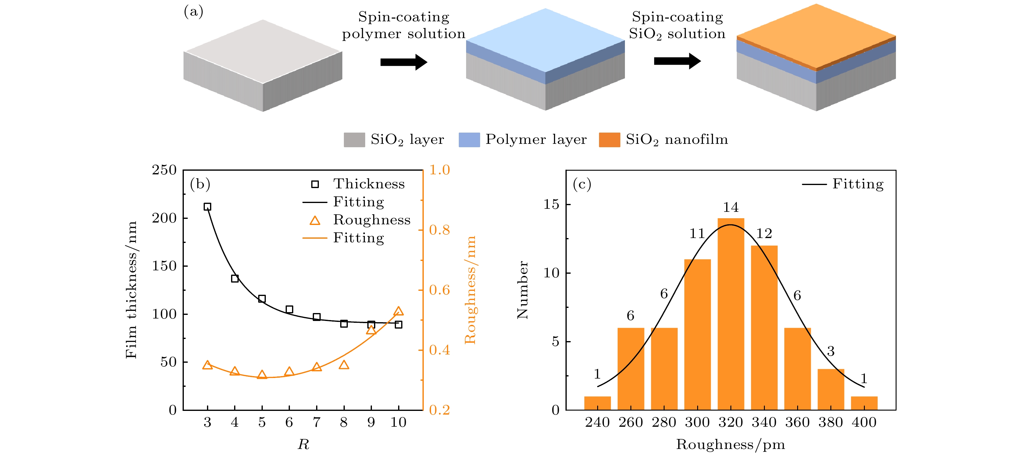
图 1 SiO2纳米薄膜的制备与表面特性 (a) 聚合物衬底制备SiO2纳米薄膜流程图; (b) SiO2纳米薄膜厚度与表面粗糙度随R值的变化; (c) R = 5条件下SiO2纳米薄膜表面粗糙度分布直方图
Fig. 1. Preparation and surface characteristics of SiO2 nanofilms: (a) Preparation process of SiO2 nanofilms on polymer substrates; (b) variation of SiO2 nanofilm thickness and surface roughness with R values; (c) histogram of surface roughness distribution of SiO2 nanofilms under the condition of R = 5.
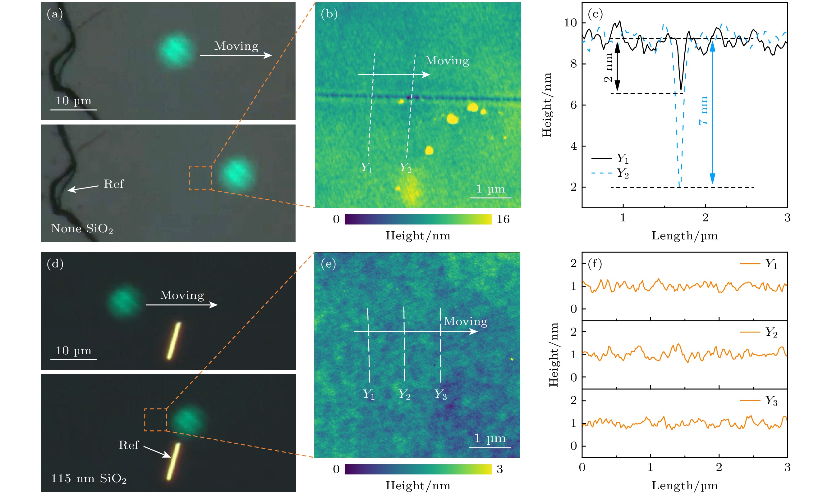
图 2 有/无SiO2纳米薄膜的PMMA上的运动痕迹比较(虚线参量Y代表数据测量位置) (a)—(c) 无SiO2纳米薄膜的PMMA上运动的光学显微图与AFM 扫描结果; (d)—(f) 115 nm厚的SiO2纳米薄膜的PMMA上运动的光学显微图与AFM 扫描结果
Fig. 2. Comparison of motion traces on PMMA with/without SiO2 nanofilms (the dashed parameter Y denotes the location of data measurement): (a)–(c) Optical micrographs and AFM scanning results of motion traces on PMMA without SiO2 nanofilm; (d)–(f) optical micrographs and AFM scanning results of motion traces on PMMA with a 115 nm-thick SiO2 nanofilm.
图 3 金纳米片单次光热冲击时衬底各层温度场分布仿真 (白色十字准线和绿色虚线圈分别代表物体质心和光斑) 金纳米片在无SiO2纳米薄膜 (a)和90 nm 厚的SiO2纳米薄膜(b)的PMMA上进行单次光热冲击时衬底各层温度分布模拟图和表面最高温度分布图; (c) 脉冲时间44.8 ns时金纳米片表面的温度分布模拟图; (d) SiO2纳米薄膜的厚度与T1, T2, ∆t的关系图, 其中T1 为SiO2纳米薄膜表面最高温度, T2为PMMA衬底表面最高温度, ∆t为滞后的时间
Fig. 3. Simulation of the temperature field distribution across substrate layers during a single photothermal shock of gold nanosheets (the white crosshairs and the green dotted circles denote the object's center of mass and the light spots, respectively): Simulation of temperature distribution across substrate layers and surface peak temperature distribution during a single photothermal shock of a gold nanosheet on PMMA without SiO2 nanofilms (a) and with a 90 nm-thick SiO2 nanofilm (b); (c) simulated temperature distribution on the surface of the gold nanosheet at a pulse duration of 44.8 ns; (d) relationship diagram between the SiO2 nanofilm thickness and T1, T2, ∆t, where T1 represents the maximum temperature on the surface of the SiO2 nanofilm, T2 represents the maximum temperature on the surface of the PMMA, and ∆t represents the time delay.
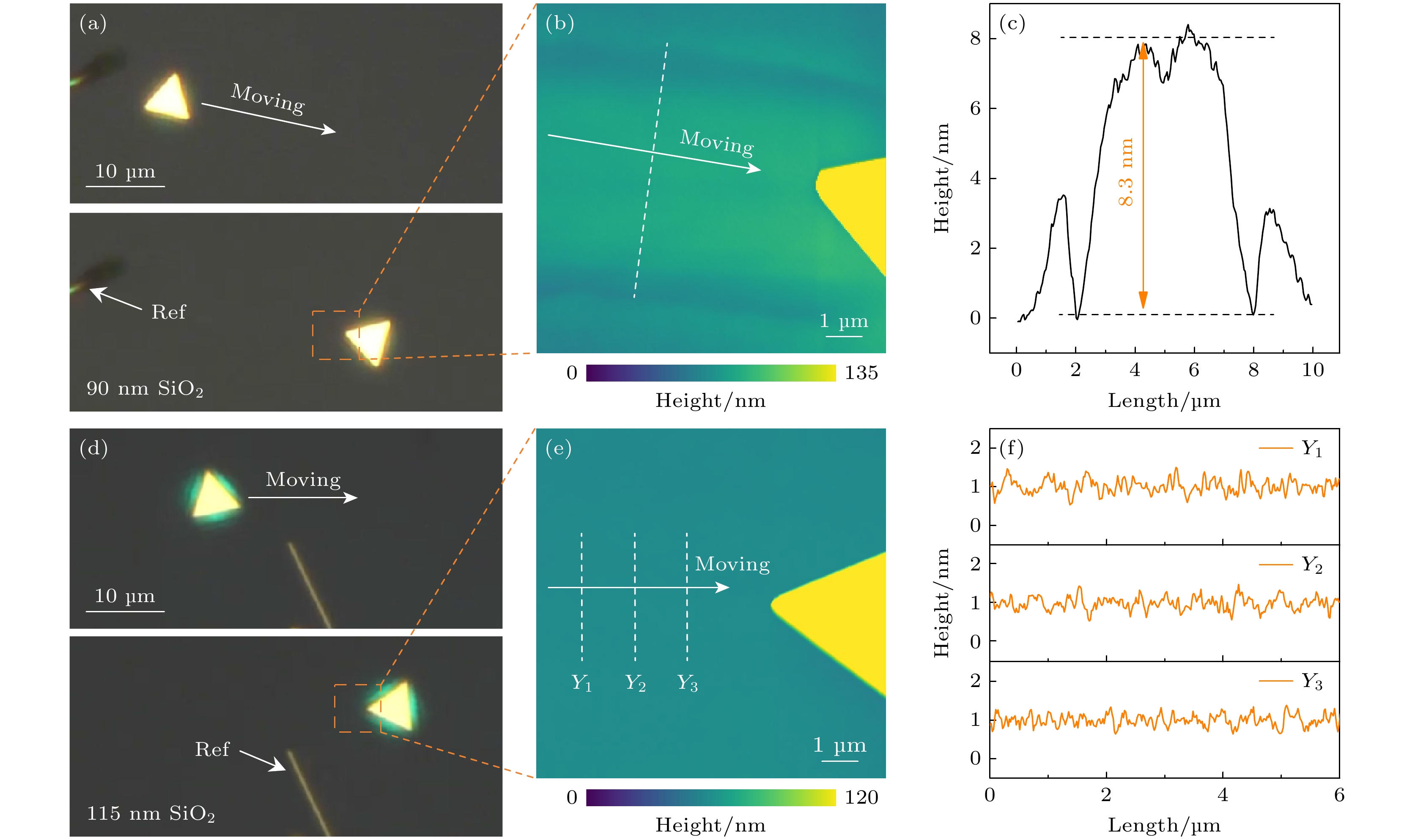
图 4 不同厚度SiO2纳米薄膜的PMMA上金纳片的运动痕迹比较(虚线参量Y代表数据测量位置) (a)—(c) 90 nm 厚的SiO2纳米薄膜的PMMA 上金纳片运动痕迹的光学显微图与AFM 扫描结果; (d)—(f) 115 nm 厚的SiO2纳米薄膜的PMMA上金纳片运动痕迹的光学显微图与AFM 扫描结果
Fig. 4. Comparison of motion traces of gold nanosheets on PMMA with SiO2 nanofilms of different thicknesses (the dashed parameter Y denotes the location of data measurement): (a)–(c) Optical micrographs and AFM scanning results of motion traces of a gold nanosheet on PMMA with a 90 nm-thick SiO2 nanofilm; (d)–(f) optical micrographs and AFM scanning results of motion traces of a gold nanosheet on PMMA with a 115 nm-thick SiO2 nanofilm.
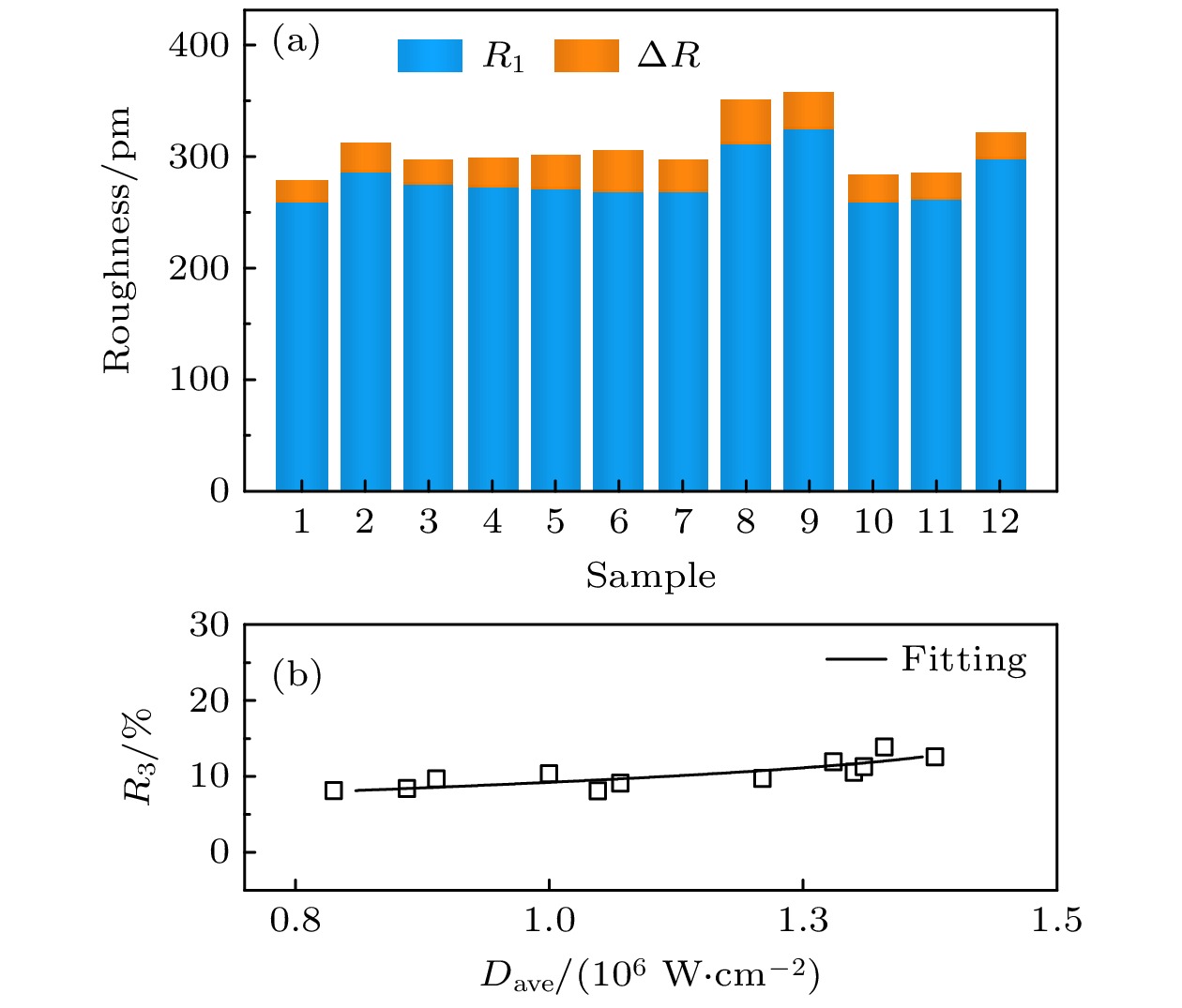
图 5 金纳米结构运动路径前后的表面粗糙度对比 (a) 金纳米结构的R1与∆R数据统计; (b) 激光平均功率密度与衬底表面粗糙度相对变化量的关系图
Fig. 5. Comparison of surface roughness before and after the motion path of gold nanostructures: (a) Statistical data of R1 and ∆R for gold nanostructures; (b) relationship diagram between the average laser power density and the relative variation in the substrate surface roughness.
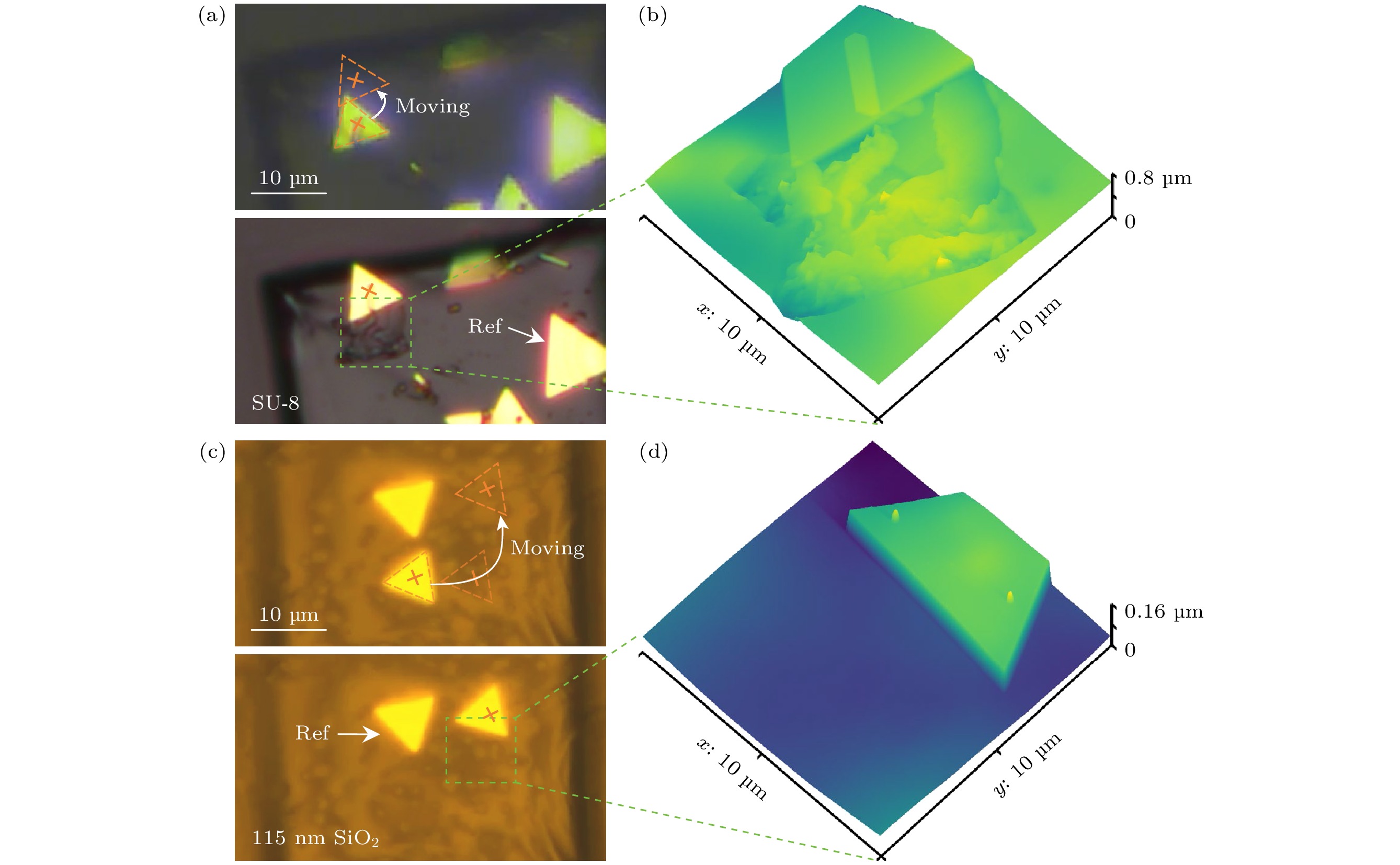
图 6 有/无SiO2纳米薄膜的SU-8上金纳片的运动痕迹比较 (橙色十字准线和橙色虚线三角形分别代表物体质心和金纳米片) (a), (b) 无SiO2纳米薄膜的SU-8上金纳米片运动痕迹的光学显微图与AFM 表面形貌图; (c), (d) 115 nm 厚的SiO2纳米薄膜的SU-8上捕获金纳米片运动痕迹的光学显微图与AFM表面形貌图
Fig. 6. Comparison of motion traces of gold nanosheets on SU-8 with/without SiO2 (The orange crosshair and the orange dashed triangle represent the centroid of the object and the gold nanosheet, respectively): (a), (b) Optical micrographs and AFM surface morphology of motion traces of a gold nanosheet on SU-8 without SiO2 nanofilms; (c), (d) optical micrographs and AFM surface morphology of motion traces of a gold nanosheet on SU-8 with a 115 nm-thick SiO2 nanofilm.
-
[1] Li N, Zhu X M, Li W Q, Fu Z H, Hu M Z, Hu H Z 2019 Front. Inform. Technol. Electron. Eng. 20 655
Google Scholar
[2] 汪涵聪, 李志鹏 2019 68 144101
Google Scholar
Wang H C, Li Z P 2019 Acta Phys. Sin. 68 144101
Google Scholar
[3] 韩翔, 陈鑫麟, 熊威, 邝腾芳, 陈志洁, 彭妙, 肖光宗, 杨开勇, 罗晖 2021 中国激光 48 0401011
Google Scholar
Han X, Chen X L, Xiong W, Kuang T F, Chen Z H, Peng M, Xiao G Z, Yang K Y, Luo H 2021 Chin. J. Lasers 48 0401011
Google Scholar
[4] Gieseler J, Gomez-Solano J R, Magazzù A, Pérez Castillo I, Pérez García L, Gironella-Torrent M, Viader-Godoy X, Ritort F, Pesce G, Arzola A V, Volke-Sepúlveda K, Volpe G 2021 Adv. Opt. Photonics 13 74
Google Scholar
[5] Yu S L, Lu J S, Ginis V, Kheifets S, Lim S W D, Qiu M, Gu T, Hu J J, Capasso F 2021 Optica 8 409
Google Scholar
[6] 徐孝浩, 高文禹, 李添悦, 邵天骅, 李星仪, 周源, 高歌泽, 王国玺, 严绍辉, 王漱明, 姚保利 2024 光学学报 44 0500001
Google Scholar
Xu X H, Gao W Y, Li T Y, Shao T H, Li X Y, Zhou Y, Gao G Z, Wang G X, Yan S H, Wang S M, Yao B L 2024 Acta Opt. Sin. 44 0500001
Google Scholar
[7] 杨嘉豪, 邓如平, 汪先友, 张聿全, 袁小聪, 闵长俊 2024 中国激光 51 62
Google Scholar
Yang J H, Deng R P, Wang X Y, Zhang Y Q, Yuan X C, Min C J 2024 Chin. J. Lasers 51 62
Google Scholar
[8] Jia Q, Lyu W, Yan W, Tang W, Lu J, Qiu M 2023 Photonics Insights 2 R05-1
Google Scholar
[9] 刘鸿江, 刘逸飞, 谷付星 2024 73 104207
Google Scholar
Liu H J, Liu Y F, Gu F X 2024 Acta Phys. Sin. 73 104207
Google Scholar
[10] Gu Z Q, Zhu R L, Shen T C, Dou L, Liu H J, Liu Y F, Liu X, Liu J, Zhuang S L, Gu F X 2023 Nat. Commun. 14 7663
Google Scholar
[11] 张尹峥, 刘鸿江, 朱润琳, 刘逸飞, 谷付星 2024 中国激光 51 1507403
Google Scholar
Zhang Y Z, Liu H J, Zhu R L, Liu Y F, Gu F X 2024 Chinese Journal of Lasers 51 1507403
Google Scholar
[12] Shi Z X, Shen T C, Dou L, Gu Z Q, Zhu R L, Dong X Y, Gu F X 2024 Laser. Photonics. Rev. 18 2400384
Google Scholar
[13] Zhu R L, Shen T C, Gu Z Q, Shi Z X, Dou L, Liu Y F, Zhuang S L, Gu F X 2024 ACS Nano 18 23232
Google Scholar
[14] Gu Z Q, Dou L, Linghu S Y, Zhu R L, Gu F X 2024 Phys. Rev. Appl. 22 054066
Google Scholar
[15] Song J K, Kim M S, Yoo S, Koo J H, Kim D H 2021 Nano Res. 14 2919
Google Scholar
[16] 谭文胜, 周建忠, 黄舒, 盛杰, 徐家乐 2016 红外与激光工程 45 67
Google Scholar
Tan W S, Zhou J Z, Huang S, Sheng J, Xu J L 2016 Infrared and Laser Engineering 45 67
Google Scholar
[17] 唐枫, 潘登, 俞飞, 黄锟境, 胡衍雷, 吴东, 李家文 2024 中国激光 51 1202401
Google Scholar
Tang F, Pan D, Yu F, Huang K J, Hu Y L, Wu D, Li J W 2024 Chin. J. Lasers 51 1202401
Google Scholar
[18] Bian P, Hu Z Y, An R, Tian Z N, Liu X Q, Chen Q D 2024 Laser Photonics Rev. 18 2300957
Google Scholar
[19] 王裕鑫, 廖常锐, 邹梦强, 包维佳, 刘德军, 张立, 王义平 2024 中国激光 51 1202409
Google Scholar
Wang Y X, Liao C R, Zou M Q, Bao W J, Liu D J, Zhang L, Wang Y P 2024 Chin. J. Lasers 51 1202409
Google Scholar
[20] Lee J, Kim J, Lee B J, Lee J, Lee H W, Hong M H, Park H H, Shim D Il, Cho H H, Kwon K H 2018 Thin Solid Films 660 715
Google Scholar
[21] 唐天同, 王兆宏 2010微纳加工科学原理(北京: 电子工业出版社) 第312页
Tang T T, Wang Z H 2010 The Science of Micro- and Nano-fabrication (Beijing: Publishing House of Electronics Industry) p312
[22] Xing A, Gao Y, Yin J G, Ren G J, Liu H T, Ma M J 2010 Appl. Surf. Sci. 256 6133
Google Scholar
[23] Kim S H, Hwang G S, Koo D, Seo D H, Kwon Y P, Lee H, Park H, Jeon E C, Kim J Y 2022 Nano Res. 15 7476
Google Scholar
[24] Li T Y, Kingsley-Smith J J, Hu Y H, Xu X H, Yan S H, Wang S M, Yao B L, Wang Z L, Zhu S N 2023 Opt. Lett. 48 255
Google Scholar
[25] Li T Y, Xu H H, Panmai M, Shao T H, Gao G Z, Xu F, Hu G W, Wang S N, Wang Z L, Zhu S N 2024 Ultrafast Sci. 4 0074
Google Scholar
[26] Li T Y, Liu M J, Hou J H, Yang X, Wang S B, Wang S M, Zhu S N, Tsai D P, Wang Z L 2024 Chip 3 100109
Google Scholar
[27] Guo J K, Sandaruwan W D N, Li J W, Ling J Z, Yuan Y, Liu X, Li Q, Wang X R 2024 Micromachines 15 337
Google Scholar
[28] Liang Z S, Zhang B L, Yi S H, Sun K Y, Pei G H, Shang Y, Liu X Y, Ren S X, Liu P F, Zhao J J 2024 Nano Mater. Sci (In press
Google Scholar
[29] Cheng Q L, Lu X Q, Tai Y H, Luo T T, Yang R H 2024 ACS Biomater. Sci. Eng. 10 5562
Google Scholar
[30] Hou J Y, Liu H T, Huang L T, Wu S B, Zhang Z L 2024 Chem. Eng. J. 498 155135
Google Scholar


 下载:
下载:


计量
- 文章访问数: 1003
- PDF下载量: 51
- 被引次数: 0
