-
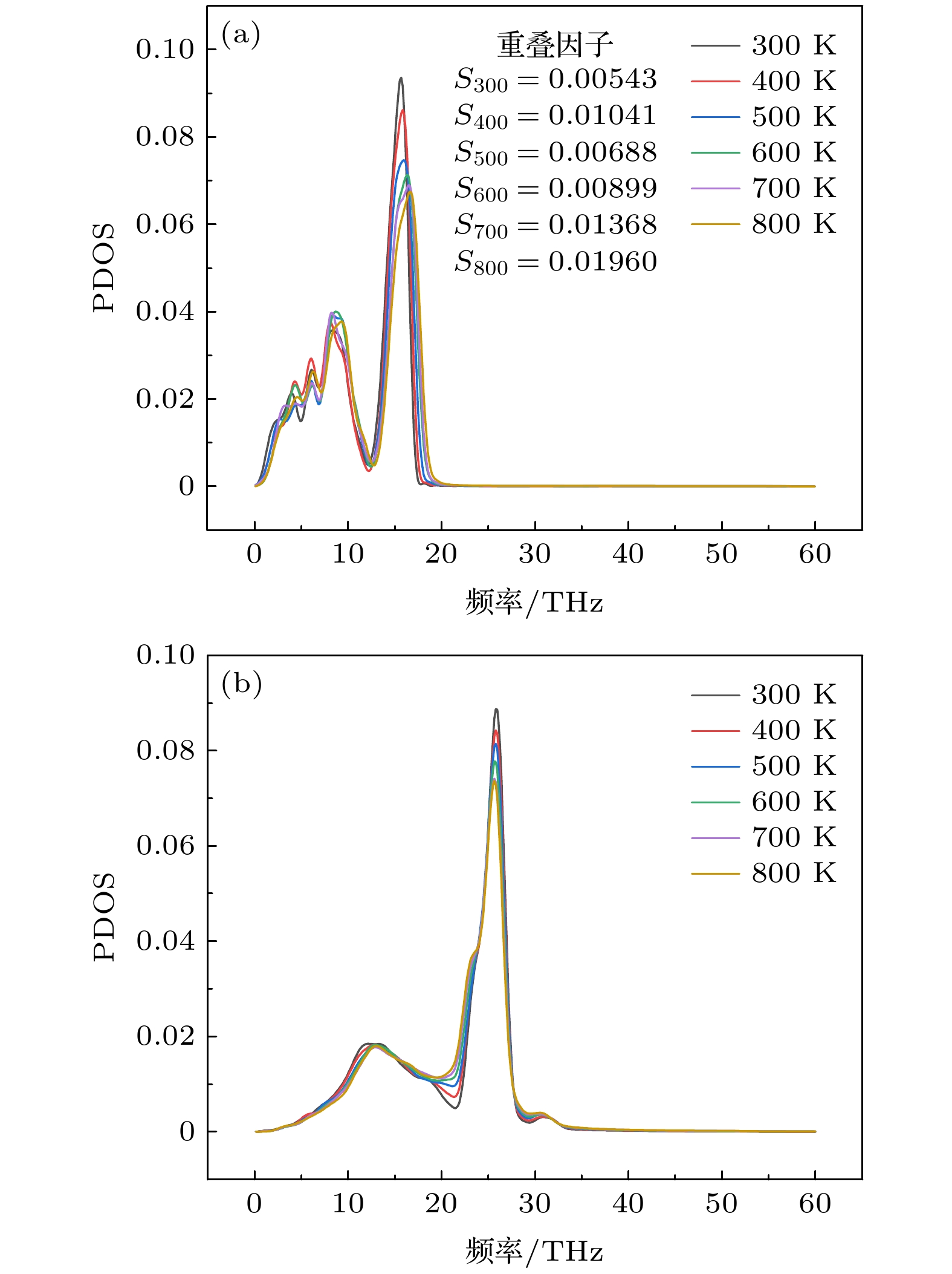
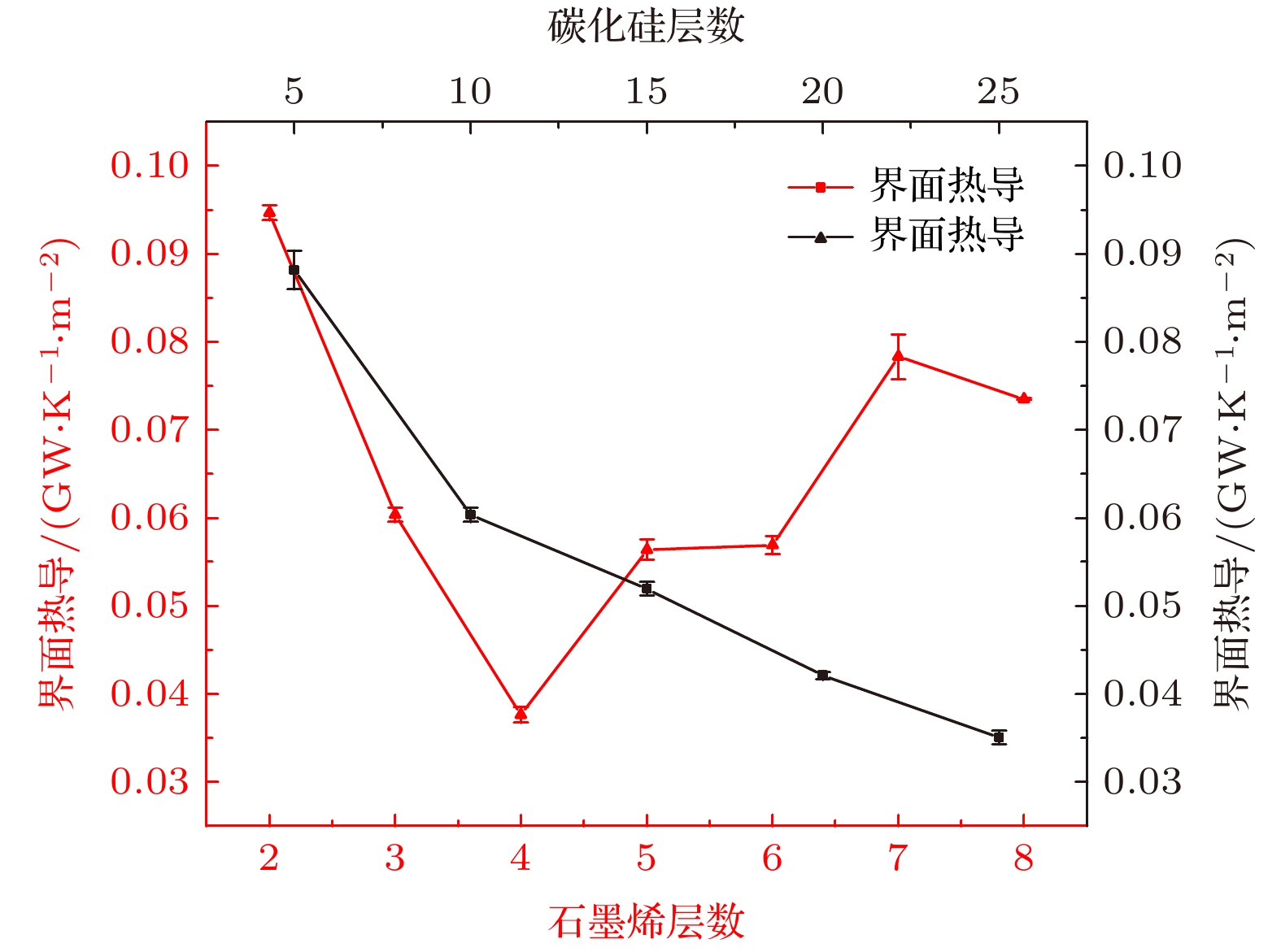
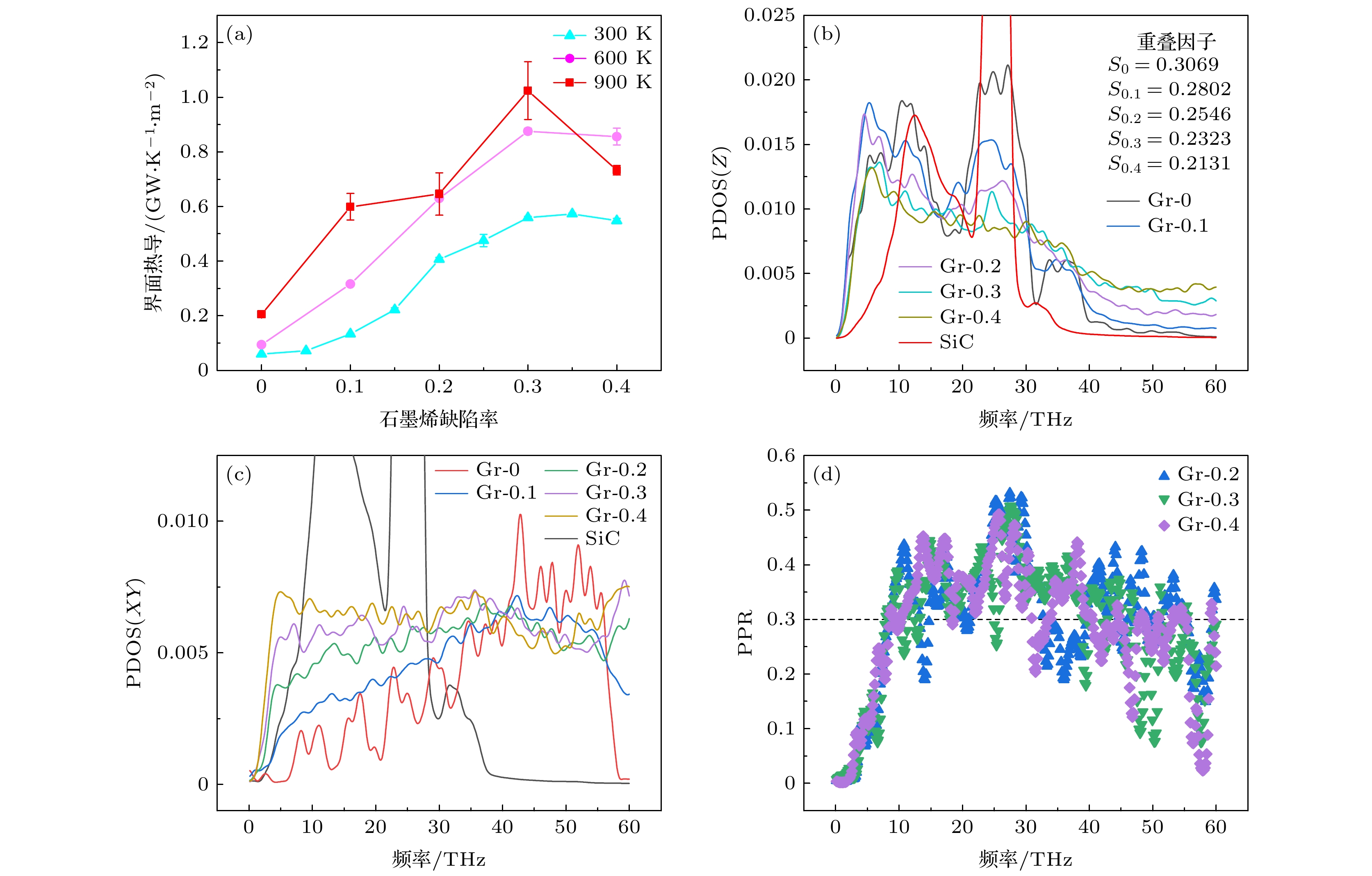
为了调控石墨烯/碳化硅异质界面传热特性, 采用非平衡态分子动力学方法研究温度、尺寸、材料缺陷率对界面热导的影响, 通过声子态密度和声子参与率对界面热导变化的原因进行阐述分析. 研究表明: 两种界面作用力下界面热导均随温度升高而增大, 但共价键的异质界面热导要高于范德瓦耳斯作用力下的界面热导. 异质界面的界面热导随着碳化硅层数的增加而降低, 当层数从10层增加到20层时, 界面热导下降30.5%; 4层时异质结构界面热导最低, 分析认为中低频段更多的声子从局域进入离域模式. 空位缺陷的引入可以有效地提高界面热导, 随着碳化硅和石墨烯缺陷率的增加, 界面热导均先升高再降低. 300 K时当碳化硅和石墨烯缺陷率分别为20%和35%时界面热导达到最大值, 分析认为缺陷的引入会阻碍中频声子的热输运. 研究结果揭示可以通过尺寸效应和空位缺陷来进行异质界面的改性研究, 有利于第三代半导体微纳器件的设计和热管理.In order to regulate thermal transfer characteristics of graphene/silicon carbide heterogeneous interface, the influence of temperature, size and material defect rate on thermal conductance of heterogeneous interface are studied by the non-equilibrium molecular dynamics method. The sandwich model of graphene/silicon carbide heterostructures with different lengths and thickness is built by Material Studio. The reasons for the change of thermal conductance are analyzed from the two aspects of phonon density of states and phonon participation rate. When the system temperature is below the Debye temperature of silicon carbide and graphene, the quantum corrections is used to calculate the thermal conductance of heterostructure in the paper. The results show that the thermal conductance increases with the increase of temperature under both interfacial forces, but the thermal conductance of heterogeneous interface under covalent bond is higher than under van der Waals force. The main reason is that the density of states of graphene in a range of 10—30 THz increases significantly with the increase of temperature. The thermal conductance of heterogeneous interface decreases with the increase of silicon carbide layers, and decreases by 30.5% when the number of silicon carbide layers increases from 10 to 20. The thermal conductance of heterostructure is the lowest in the thermal conductances of 4 layers, it is considered that more phonons are transferred from local to delocalized mode in the middle and low frequency band. The introduction of vacancy defects can effectively improve the interface thermal conductance. At different temperatures, the interfacial thermal conductance first increases and then decreases with the increase of graphene defects, and the defect rate when the interfacial thermal conductance reaches the maximum value and the degree of interfacial thermal conductance decrease after reaching the maximum value is related to temperature. When the defect rate of silicon carbide and graphene are 20% and 35% respectively at 300 K, the interface thermal conductance reaches a maximum value. When the temperature is 900 K, the thermal conductance of graphene/silicon carbide heterogeneous interface reaches a maximum value when the defect rate is 30%. It is considered that the introduction of defects will hinder the medium frequency phonons from realizing the heat transport. The results show that the size effect and vacancy defect can be utilized to modify the heterogeneous interface, which is beneficial to the design and thermal management of the third-generation semiconductor micro-nano devices.
-
Keywords:
- heterogeneous interface /
- size effect /
- vacancy defect /
- thermal conductance
[1] Nguyen M H, Kwak S 2020 Electronics 9 2068
 Google Scholar
[2] Tsunenobu K, Heiji W 2020 Appl. Phys. Exp. 13 120101
 Google Scholar
[3] So T, Takahiro Y, Jun N, Takahisa O, Chioko K, Asuka H, Satoshi I 2018 Phys. Rev. B 97 125411
 Google Scholar
[4] Inoue M, Kageshima H, Kangawa Y, Kakimoto K 2012 Phys. Rev. B 86 085417
 Google Scholar
[5] Wang Z, Bi K, Guan H W, Wang J 2014 J. Mater. 2014 479808
 Google Scholar
[6] Wang Z, Guan H W 2014 Appl. Mech. Mater. 2943 63
 Google Scholar
[7] Wang Y W, Guo X N, Dong L L, Jin G Q, Wang Y Y, Guo X Y 2013 Int. J. Hydrogen Energy 38 12733
 Google Scholar
[8] Lai S K, Arifin R, Jakse N 2011 Condens. Matter Phys. 14 43802
 Google Scholar
[9] Yue Y N, Zhang J C, Wang X W 2011 Small 7 3324
 Google Scholar
[10] Guo Z X, Ding J W, Gong X G 2012 Phys. Rev. B 85 235429
 Google Scholar
[11] Li M, Yue Y N 2014 RSC. Adv. 4 23010
 Google Scholar
[12] Liang T, Zhang P, Yuan P, Zhai S P, Yang D G 2019 Nano Futures. 3 15004
[13] Liang T, Zhou M, Zhang P, Yuan P, Yang D G 2020 Int. J. Heat Mass Transfer 151 119395
[14] Wang Y C, Zhu Y B, He Z Z, Wu H A 2020 Ceram. Int. 46 29101
 Google Scholar
[15] Gao Y, Xu B X 2018 ASC Nano 12 11254
 Google Scholar
[16] Gao Y, Xu B X 2018 ACS Appl. Mater. Interfaces 16 14221
 Google Scholar
[17] Cui L, Wei G S, Li Z, Du X Z 2021 Int. J. Heat Mass Transfer 165 120685
 Google Scholar
[18] Nguyen D T, Le M Q, Bui T L, Bui H L 2017 Acta Mech. Sin. 33 132
 Google Scholar
[19] Hu X L, Lee J, Berman D, Martini A 2018 Carbon 137 118
 Google Scholar
[20] Adrien A, Jiahao K, Kaustav B, Andras K 2015 Nat. Mater. 14 1195
 Google Scholar
[21] Lin Z Y, Ji L F, Yan T Y, Xu Y B, Sun Z Y 2020 J. Mater. Res. Technol. 9 5934
 Google Scholar
[22] 杨平, 王晓亮, 李培, 王欢, 张立强, 谢方伟 2012 61 076501
 Google Scholar
Yang P, Wang X L, Li P, Wang H, Zhang L Q, Xie F W 2012 Acta Phys. Sin. 61 076501
 Google Scholar
[23] Liu D J 2020 Phys. Lett. A 384 126077
[24] Li M, Zhang J C, Hu X J, Yue Y N 2015 Appl. Phys. A 119 415
 Google Scholar
[25] Guénolé J, Nöhring W G, Vaid A, Houllé F, Xie Z C, Prakash A, Bitzek E 2020 Comput. Mater. Sci. 175 109584
 Google Scholar
[26] Hammond K D 2020 Comput. Phys. Commun. 247 106862
 Google Scholar
[27] Li Z, Xiong S Y, Sievers C, Hu Y, Fan Z Y, Wei N, Bao H, Chen S D, Donadio D, Ala-Nissila T 2019 J. Chem. Phys. 151 234105
[28] Mao R, Kong B D, Kim K W, Jayasekera T, Calzolari A, Buongiorno M, Nardelli 2012 Appl. Phys. Lett. 101 113111
 Google Scholar
[29] Wang H, Gong J, Pei Y, Xu Z 2013 ACS Appl. Mater.Interfaces 5 2599
 Google Scholar
-
图 9 (a)不同温度下石墨烯缺陷对界面热导的影响; (b)不同石墨烯陷率下对应的面外方向(Z) PDOS的变化情况(温度为300 K); (c)不同石墨烯陷率下对应的面内方向(XY) PDOS的变化情况(温度为300 K); (d)缺陷率分别为20%—40%时石墨烯PPR的变化情况
Fig. 9. (a) Effect of graphene defects on the thermal conductance of the interface at different temperatures; (b) the change of PDOS in the out of plane direction (Z) under different graphene defects rates at the temperature of 300 K; (c) the change of PDOS in the in-plane direction (XY) under different graphene defects rates at the temperature of 300 K; (d) the change of PPR of graphene with defect rate of 20%–40%.
-
[1] Nguyen M H, Kwak S 2020 Electronics 9 2068
 Google Scholar
[2] Tsunenobu K, Heiji W 2020 Appl. Phys. Exp. 13 120101
 Google Scholar
[3] So T, Takahiro Y, Jun N, Takahisa O, Chioko K, Asuka H, Satoshi I 2018 Phys. Rev. B 97 125411
 Google Scholar
[4] Inoue M, Kageshima H, Kangawa Y, Kakimoto K 2012 Phys. Rev. B 86 085417
 Google Scholar
[5] Wang Z, Bi K, Guan H W, Wang J 2014 J. Mater. 2014 479808
 Google Scholar
[6] Wang Z, Guan H W 2014 Appl. Mech. Mater. 2943 63
 Google Scholar
[7] Wang Y W, Guo X N, Dong L L, Jin G Q, Wang Y Y, Guo X Y 2013 Int. J. Hydrogen Energy 38 12733
 Google Scholar
[8] Lai S K, Arifin R, Jakse N 2011 Condens. Matter Phys. 14 43802
 Google Scholar
[9] Yue Y N, Zhang J C, Wang X W 2011 Small 7 3324
 Google Scholar
[10] Guo Z X, Ding J W, Gong X G 2012 Phys. Rev. B 85 235429
 Google Scholar
[11] Li M, Yue Y N 2014 RSC. Adv. 4 23010
 Google Scholar
[12] Liang T, Zhang P, Yuan P, Zhai S P, Yang D G 2019 Nano Futures. 3 15004
[13] Liang T, Zhou M, Zhang P, Yuan P, Yang D G 2020 Int. J. Heat Mass Transfer 151 119395
[14] Wang Y C, Zhu Y B, He Z Z, Wu H A 2020 Ceram. Int. 46 29101
 Google Scholar
[15] Gao Y, Xu B X 2018 ASC Nano 12 11254
 Google Scholar
[16] Gao Y, Xu B X 2018 ACS Appl. Mater. Interfaces 16 14221
 Google Scholar
[17] Cui L, Wei G S, Li Z, Du X Z 2021 Int. J. Heat Mass Transfer 165 120685
 Google Scholar
[18] Nguyen D T, Le M Q, Bui T L, Bui H L 2017 Acta Mech. Sin. 33 132
 Google Scholar
[19] Hu X L, Lee J, Berman D, Martini A 2018 Carbon 137 118
 Google Scholar
[20] Adrien A, Jiahao K, Kaustav B, Andras K 2015 Nat. Mater. 14 1195
 Google Scholar
[21] Lin Z Y, Ji L F, Yan T Y, Xu Y B, Sun Z Y 2020 J. Mater. Res. Technol. 9 5934
 Google Scholar
[22] 杨平, 王晓亮, 李培, 王欢, 张立强, 谢方伟 2012 61 076501
 Google Scholar
Yang P, Wang X L, Li P, Wang H, Zhang L Q, Xie F W 2012 Acta Phys. Sin. 61 076501
 Google Scholar
[23] Liu D J 2020 Phys. Lett. A 384 126077
[24] Li M, Zhang J C, Hu X J, Yue Y N 2015 Appl. Phys. A 119 415
 Google Scholar
[25] Guénolé J, Nöhring W G, Vaid A, Houllé F, Xie Z C, Prakash A, Bitzek E 2020 Comput. Mater. Sci. 175 109584
 Google Scholar
[26] Hammond K D 2020 Comput. Phys. Commun. 247 106862
 Google Scholar
[27] Li Z, Xiong S Y, Sievers C, Hu Y, Fan Z Y, Wei N, Bao H, Chen S D, Donadio D, Ala-Nissila T 2019 J. Chem. Phys. 151 234105
[28] Mao R, Kong B D, Kim K W, Jayasekera T, Calzolari A, Buongiorno M, Nardelli 2012 Appl. Phys. Lett. 101 113111
 Google Scholar
[29] Wang H, Gong J, Pei Y, Xu Z 2013 ACS Appl. Mater.Interfaces 5 2599
 Google Scholar
计量
- 文章访问数: 10260
- PDF下载量: 490
- 被引次数: 0


 下载:
下载:


