-
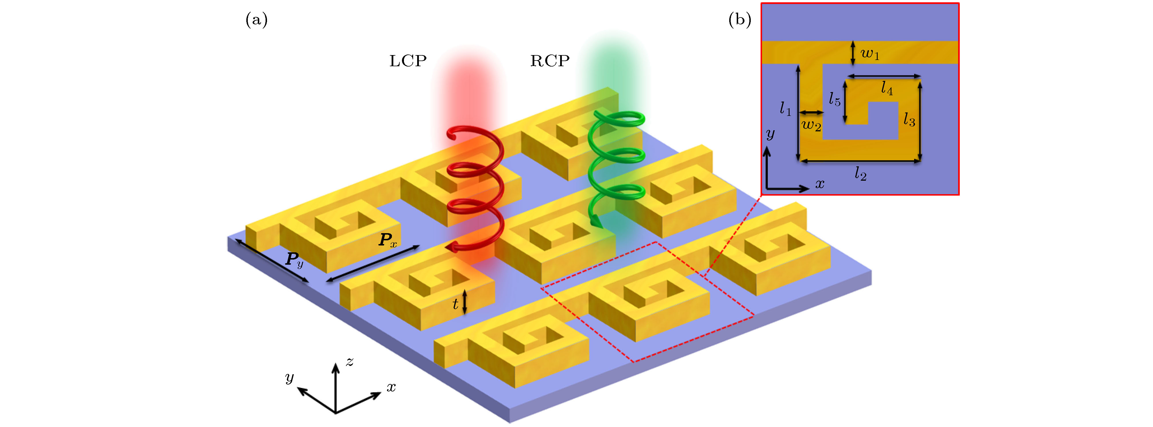
圆二色性效应在圆偏振器、光调制器及光电器件等方面具有广泛的应用. 为提高平面金属微纳结构的圆二色性, 本文设计了由无限长纳米线和G形微纳结构组成的平面复合金属微纳结构, 并应用有限元方法研究了该阵列微纳结构的圆二色性特性. 数值计算结果显示, 在圆偏振光的激发下, G形微纳结构和平面复合金属微纳结构均出现了电偶极子、电四极子和电八极子等共振模式. 当G形微纳结构与无限长纳米线连接时, 各共振波长均发生红移, 并且无限长纳米线增加了不同圆偏振光激发下的局域表面等离激元共振强度, 从而使得平面复合微纳结构的圆二色性信号明显增强. 此外, 还研究了平面复合微纳结构阵列的几何参数对其圆二色性特性的影响. 这些结果为提高平面手性微纳结构的圆二色性信号强度提供一定的指导思路和方法.Circular dichroism effects have been widely used in circular polarizers, optical modulators and optoelectronic devices. Periodically arranged artificial metal chiral nanostructures has a strong electromagnetic coupling effect with light, which can greatly increase the interaction between the light and matter. Three-dimensional helix and helix-like chiral nanostructures show a larger circular dichroism effect due to the strong interactions between electric and magnetic resonance. The double-layer structures also can produce large circular dichroism, which signals also results from electric dipoles with different orientations between the two layers. Although the three dimensional plasmonic structures have shown large circular dichroism signals, however, three dimensional devices hold disadvantages in wide practical applications because of their complicated fabricating process, especially at micro- and nanoscales. Recent years, circular dichroism signals of planar nanostructures have been studied owing to their easy fabrication and wide potential applications. The resonance mode of planar metal nanostructures is sensitive to the shape, geometry, materials and surrounding environment of nanostructures, which provides a feasible technical approach for adjusting the circular dichroism signal of planar metal nanostructures. In this article, larger circular dichroism signals are realized through planar composite golden nanostructures, which composed of infinite long nanowire and G-shaped nanostructure. The absorption spectra, surface charge distributions at resonance wavelength of planar composite golden nanostructure are calculated by finite element method. For comparison, a circular dichroism signal with only G-shaped nanostructures is also studied. The numerical results show that under the illumination of right-handed polarized and left-handed polarized light, the planar composite golden nanostructure and G-shaped nanostructure exhibit electric dipole, quadrupolar, octupolar resonance modes, respectively. When the G-shaped nanostructure is connected to an infinitely long nanowire, all resonance peaks have a red shift and infinitely long nanowire increases the local surface resonance intensity under different circularly polarized light excitation. Therefore, it significantly enhances the circular dichroism signal of the planar composite golden nanostructure. At the same time, the influence of geometric parameters such as the different length of each nanorod of the G-shaped nanostructure and the thickness of the infinitely length nanowire on the circular dichroism modes are also studied. The findings may provide some guideline and methods for improving the circular dichroism signal of planar chiral nanostructure.
-
Keywords:
- chiral nanostructure /
- absorption properties /
- circular dichroism /
- surface plasmon
[1] Zheng Z G, Li Y, Bisoyi H K, Wang L, Bunning T J, Li Q 2016 Nature 531 352
 Google Scholar
[2] Karimi E, Schulz S A, De L I, Qassim H, Upham J, Boyd R W 2014 Light-Sci. Appl. 3 167
 Google Scholar
[3] 杨傅子 2014 64 124214
 Google Scholar
Yang F Z 2014 Acta Phys. Sin. 64 124214
 Google Scholar
[4] Gansel J K, Thiel M, Rill M S, Decker M, Bade K, SaileV, Wegener M 2009 Science 325 5947
 Google Scholar
[5] Khanikaev A B, Arju N, Fan Z, Purtseladze D, Lu F, Lee J, Sarriugarte P, Schnell M, Hillenbrand R, Belkin M A, Shvets G 2016 Nat. Commun. 7 12045
 Google Scholar
[6] Sun M, Zhang Z, Wang P, Li Q, Ma F, X Hong 2013 Light-Sci. Appl. 2 e112
 Google Scholar
[7] 李杰, 杨方清, 董建峰 2011 60 124214
 Google Scholar
Li J, Yang F Q, Dong J F 2011 Acta Phys. Sin. 60 124214
 Google Scholar
[8] Pendry J B 2004 Science 306 1353
 Google Scholar
[9] 苏妍妍, 龚伯仪, 赵晓鹏 2012 61 084102
 Google Scholar
Su Y Y, Gong B Y, Zhao X P 2012 Acta Phys. Sin. 61 084102
 Google Scholar
[10] Maoz B M, Weegen R, Fan Z, Govorov A O, Ellestad G, Berova N, G Markovich 2012 J. Am. Chem. Soc. 134 17807
 Google Scholar
[11] Zhu F, Li X, Li Y, Yan M, Liu S 2014 Anal. Chem. 87 357
 Google Scholar
[12] Hendry E, Carpy T, Johnston J, Popland M, Mikhaylovskiy R V, Lapthorn A J, Kadodwala M 2010 Nat. Nanotechnol. 5 783
 Google Scholar
[13] Mochida Y, Cabral H, Miura Y, Albertini F, Fukushima S, Osada K, Kataoka K 2014 ACS Nano 8 6724
 Google Scholar
[14] Narushima T, Okamoto H 2013 J. Phys. Chem. 117 23964
 Google Scholar
[15] Narushima T, Hashiyada S, Okamoto H 2014 ACS Photonics 1 732
 Google Scholar
[16] Dietrich K, Lehr D, Helgert C, Tünnermann A, Kley E B 2012 Adv. Mater. 24 321
 Google Scholar
[17] Yin X H, Schaferling M, Metzger B, Giessen H 2013 Nano Lett. 13 6238
 Google Scholar
[18] Larsen G K, Zhao Y P 2014 Appl. Phys. Lett. 105 071109
 Google Scholar
[19] Gansel J K, Latzel M, Frolich A, Kaschke J, Thiel M, Wegener M 2015 Appl. Phys. Lett. 100 101109i
 Google Scholar
[20] Decker M, Zhao R, Soukoulis C M, Linden S, Wegener M 2010 Opt. Lett. 35 1593
 Google Scholar
[21] Liu N, Liu H, Zhu S, Giessen, Harald 2009 Nat. Photonics 3 157
 Google Scholar
[22] Jing Z, Bai Y, Wang T, Ullah H, Li Y, Zhang Z Y 2019 J. Opt. Soc. Am. B 36 2721
 Google Scholar
[23] Hwang Y, Lee Se, Kim S, Lin J, Yuan X C 2018 ACS Photonics 5 4538
 Google Scholar
[24] Valev V K, Smisdom N, Silhanek A V, Clercq B D, Gillijins W, Ameloot M, Moshchalkov V T 2009 Nano Lett. 9 3945
 Google Scholar
[25] Hendry E, Carpy T, Johnston J 2010 Nature Nanotechnology 5 783
[26] Zu S, Bao Y, Fang Z 2016 Nanoscale 8 3900
 Google Scholar
[27] Knipper R, Mayerhofer T G, Kopecky V, Huebner J U, Popp J 2018 ACS Photonics 5 1176
 Google Scholar
[28] Yannopapas V 2009 Opt. Lett. 32 632
 Google Scholar
[29] Feng C, Wang Z B, Lee S, Jiao J, Li L 2012 Opt. Commun. 2 245
 Google Scholar
[30] Yan C, Martin O J F 2014 ACS Nano 8 11860
 Google Scholar
[31] Tian X, Fang Y, Sun M 2015 Sci. Rep. 5 17534
 Google Scholar
-
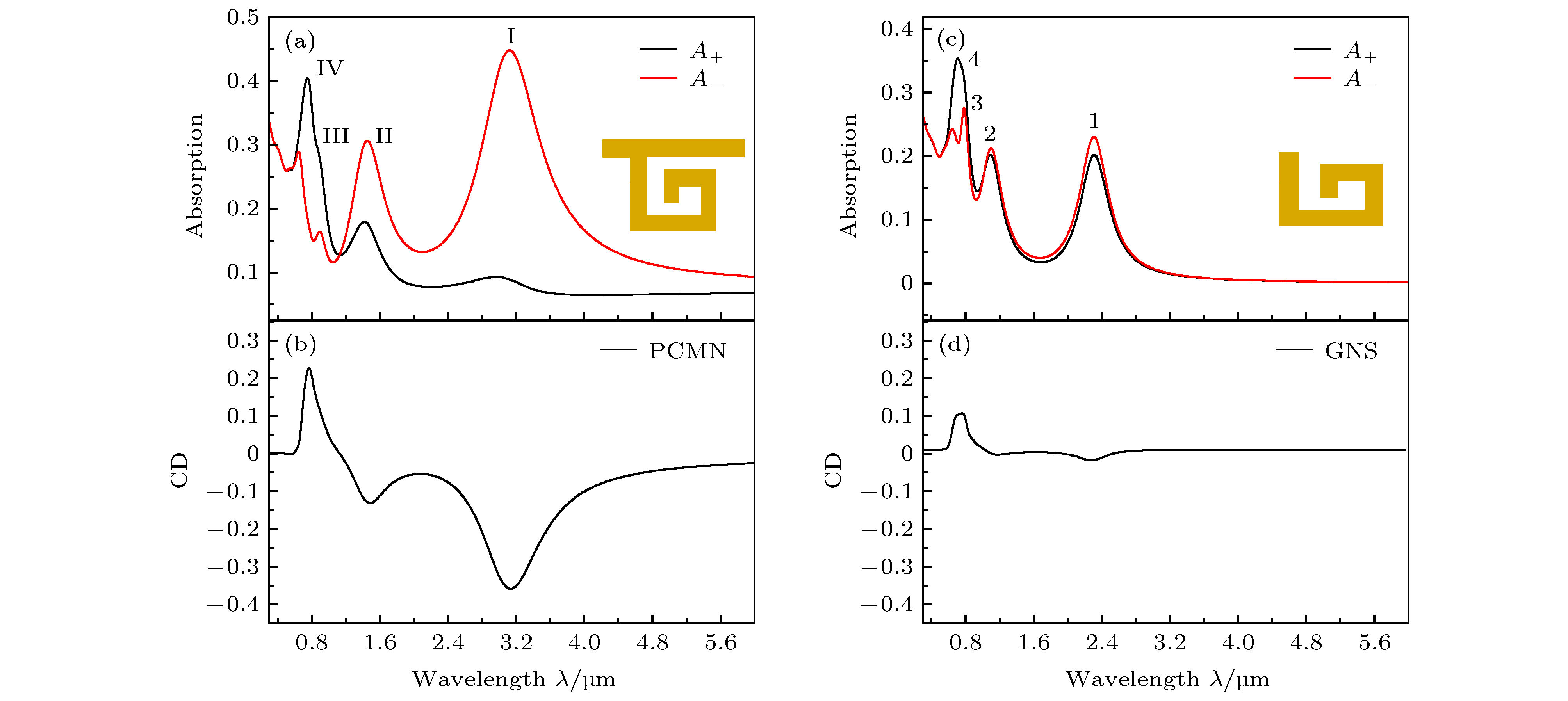
图 2 PCMN和GNS阵列的吸收光谱以及CD光谱 (a), (c) PCMN和GNS阵列的A+, A–光谱; (b), (d)PCMN阵列和GNS阵列的CD光谱; 其中插图分别表示PCMN和GNS在xy平面的结构示意图
Fig. 2. Absorption and CD spectra of PCMN and GNS arrays: (a), (c) Simulated A–, A+ spectra; (b), (d) CD spectra of PCMN and GNS arrays. The insert figures indicate the structure schematic of PCMN and GNS in x-y plane, respectively.
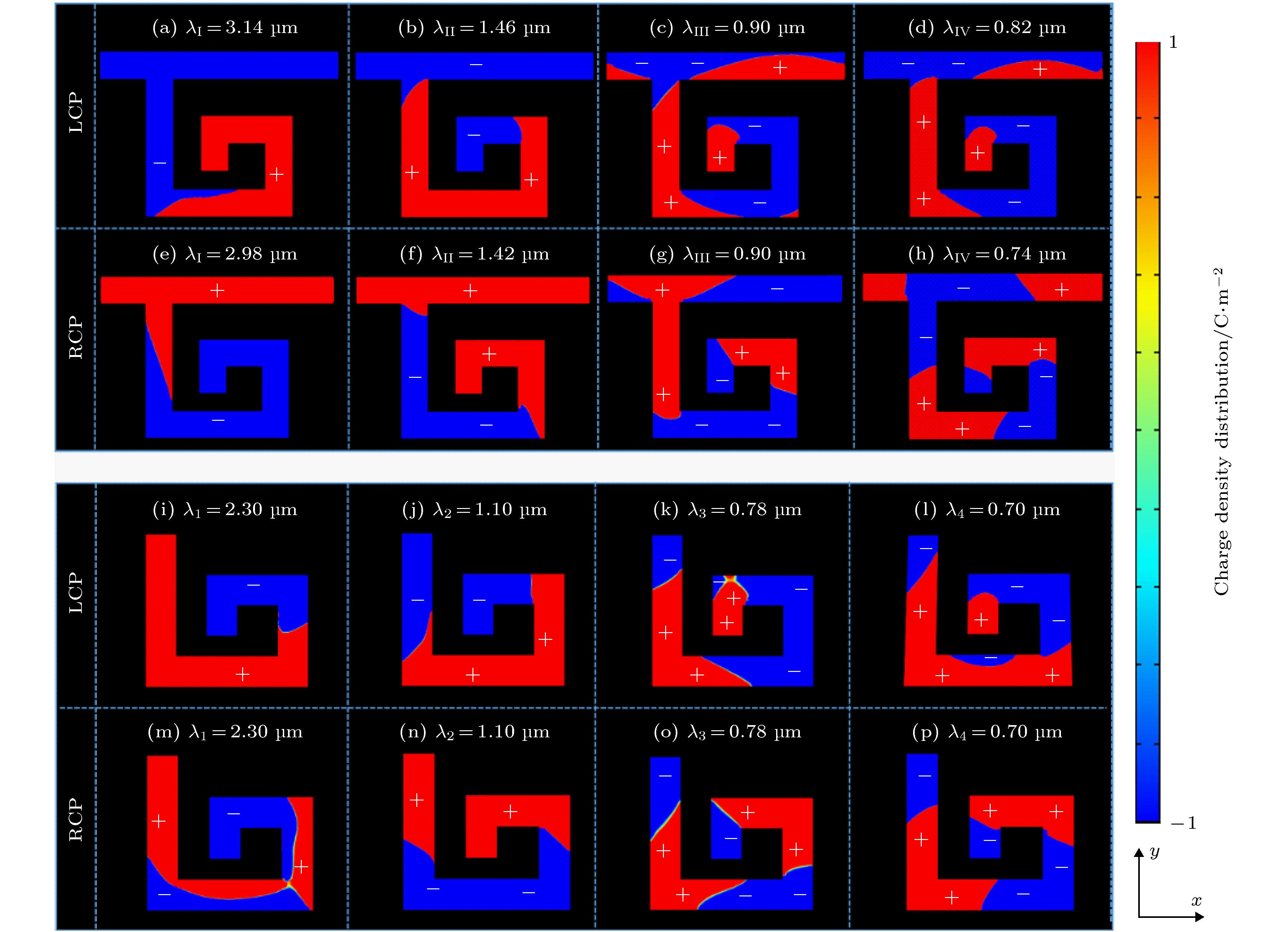
图 3 不同偏振的入射光照射在PCMN和GNS时, 在共振波长处的表面电荷密度分布; 图(a), (b), (c), (d), (i), (j), (k)和(l)是为左旋偏振光; 图(e), (f), (g), (h), (m), (n), (o)和(p)是为右旋偏振光
Fig. 3. Surface charge density distribution of proposed PCMN and GNS at the resonant wavelength with different circularly polarized illuminations: (a), (b), (c), (d), (i), (j), (k) and (l) for LCP light; (e), (f), (g), (h), (m), (n), (o) and (p) for RCP light.
图 4 PCMN阵列不同参数的CD光谱. 不同长度的(a) l1, (b) l2, (c) l3, (d) l4, (e) l5纳米棒和(f)不同无限长纳米线宽度w1的PCMN阵列的CD光谱
Fig. 4. CD spectra of PCMN arrays with different parameter; CD spectraof PCMN arrays with (a) different l1 (b) different l2, (c) different l3, (d) different l4, (e) different l5 nanorod and (f) different w1 of the infinite long nanowire.
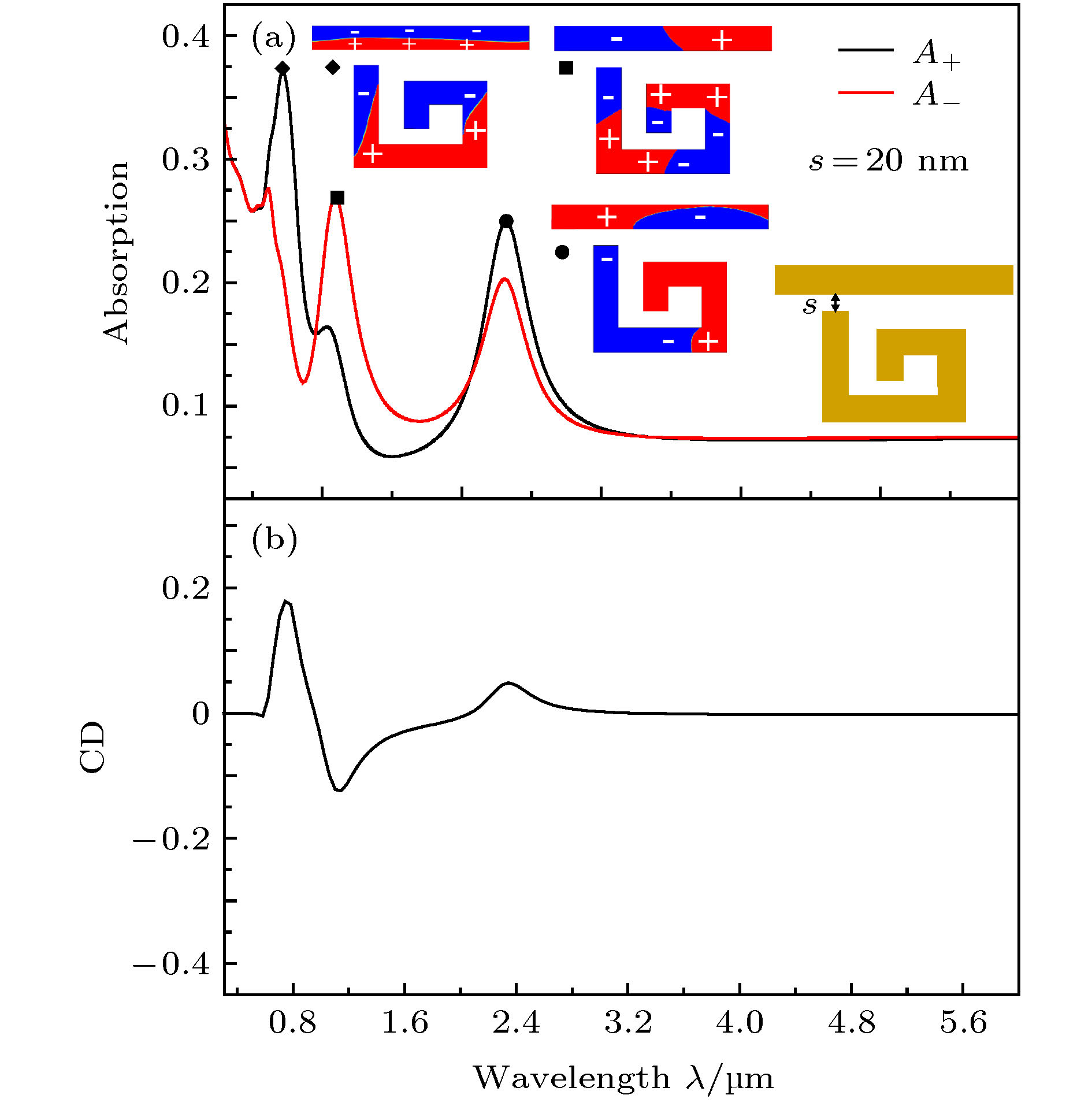
图 5 断开的PCMN阵列的吸收光谱和CD光谱 (a)吸收光谱; (b) CD光谱. 插图表示分别在共振波长处的电荷分布(深红-蓝色)和断开的PCMN在xy平面上的结构示意图(黄色)
Fig. 5. Absorption and CD spectra of the separated PCMN arrays: (a) Absorption spectrum; (b) CD spectrum; The insert figures indicate the charge distribution at resonance wavelength (crimson and blue), and structure schematic (yellow) of separated PCMN in xy plane.
-
[1] Zheng Z G, Li Y, Bisoyi H K, Wang L, Bunning T J, Li Q 2016 Nature 531 352
 Google Scholar
[2] Karimi E, Schulz S A, De L I, Qassim H, Upham J, Boyd R W 2014 Light-Sci. Appl. 3 167
 Google Scholar
[3] 杨傅子 2014 64 124214
 Google Scholar
Yang F Z 2014 Acta Phys. Sin. 64 124214
 Google Scholar
[4] Gansel J K, Thiel M, Rill M S, Decker M, Bade K, SaileV, Wegener M 2009 Science 325 5947
 Google Scholar
[5] Khanikaev A B, Arju N, Fan Z, Purtseladze D, Lu F, Lee J, Sarriugarte P, Schnell M, Hillenbrand R, Belkin M A, Shvets G 2016 Nat. Commun. 7 12045
 Google Scholar
[6] Sun M, Zhang Z, Wang P, Li Q, Ma F, X Hong 2013 Light-Sci. Appl. 2 e112
 Google Scholar
[7] 李杰, 杨方清, 董建峰 2011 60 124214
 Google Scholar
Li J, Yang F Q, Dong J F 2011 Acta Phys. Sin. 60 124214
 Google Scholar
[8] Pendry J B 2004 Science 306 1353
 Google Scholar
[9] 苏妍妍, 龚伯仪, 赵晓鹏 2012 61 084102
 Google Scholar
Su Y Y, Gong B Y, Zhao X P 2012 Acta Phys. Sin. 61 084102
 Google Scholar
[10] Maoz B M, Weegen R, Fan Z, Govorov A O, Ellestad G, Berova N, G Markovich 2012 J. Am. Chem. Soc. 134 17807
 Google Scholar
[11] Zhu F, Li X, Li Y, Yan M, Liu S 2014 Anal. Chem. 87 357
 Google Scholar
[12] Hendry E, Carpy T, Johnston J, Popland M, Mikhaylovskiy R V, Lapthorn A J, Kadodwala M 2010 Nat. Nanotechnol. 5 783
 Google Scholar
[13] Mochida Y, Cabral H, Miura Y, Albertini F, Fukushima S, Osada K, Kataoka K 2014 ACS Nano 8 6724
 Google Scholar
[14] Narushima T, Okamoto H 2013 J. Phys. Chem. 117 23964
 Google Scholar
[15] Narushima T, Hashiyada S, Okamoto H 2014 ACS Photonics 1 732
 Google Scholar
[16] Dietrich K, Lehr D, Helgert C, Tünnermann A, Kley E B 2012 Adv. Mater. 24 321
 Google Scholar
[17] Yin X H, Schaferling M, Metzger B, Giessen H 2013 Nano Lett. 13 6238
 Google Scholar
[18] Larsen G K, Zhao Y P 2014 Appl. Phys. Lett. 105 071109
 Google Scholar
[19] Gansel J K, Latzel M, Frolich A, Kaschke J, Thiel M, Wegener M 2015 Appl. Phys. Lett. 100 101109i
 Google Scholar
[20] Decker M, Zhao R, Soukoulis C M, Linden S, Wegener M 2010 Opt. Lett. 35 1593
 Google Scholar
[21] Liu N, Liu H, Zhu S, Giessen, Harald 2009 Nat. Photonics 3 157
 Google Scholar
[22] Jing Z, Bai Y, Wang T, Ullah H, Li Y, Zhang Z Y 2019 J. Opt. Soc. Am. B 36 2721
 Google Scholar
[23] Hwang Y, Lee Se, Kim S, Lin J, Yuan X C 2018 ACS Photonics 5 4538
 Google Scholar
[24] Valev V K, Smisdom N, Silhanek A V, Clercq B D, Gillijins W, Ameloot M, Moshchalkov V T 2009 Nano Lett. 9 3945
 Google Scholar
[25] Hendry E, Carpy T, Johnston J 2010 Nature Nanotechnology 5 783
[26] Zu S, Bao Y, Fang Z 2016 Nanoscale 8 3900
 Google Scholar
[27] Knipper R, Mayerhofer T G, Kopecky V, Huebner J U, Popp J 2018 ACS Photonics 5 1176
 Google Scholar
[28] Yannopapas V 2009 Opt. Lett. 32 632
 Google Scholar
[29] Feng C, Wang Z B, Lee S, Jiao J, Li L 2012 Opt. Commun. 2 245
 Google Scholar
[30] Yan C, Martin O J F 2014 ACS Nano 8 11860
 Google Scholar
[31] Tian X, Fang Y, Sun M 2015 Sci. Rep. 5 17534
 Google Scholar
计量
- 文章访问数: 9690
- PDF下载量: 180
- 被引次数: 0


 下载:
下载:


