


-
二维铁电半导体α-In2Se3在新型电子器件中具有重要应用前景. 然而采用化学气相沉积法(CVD), 该材料通常需要高于650 ℃的高温. 本研究提出一种低温合成策略, 通过引入KCl/LiCl/NH4Cl三元催化剂体系, 在400—460 ℃ (优化条件440 ℃)制备α-In2Se3薄膜, 该工艺较传统方法降低温度200 ℃以上. 扫描电子显微镜(SEM)表征显示材料形貌可通过温度与气体流速协同调控, 从六边形薄片转变为连续均匀薄膜; 能量色散谱仪(EDS)分析表明元素比例接近理想化学计量比(In∶Se = 36.38∶63.62); 拉曼光谱(特征峰103/180/195 cm–1) 与X射线光电子能谱(XPS) (In∶Se = 1.92∶3.00) 共同证实材料为纯α相、化学计量比接近理想值. 基于此材料构建的阻变器件表现出模拟阻变的特性, 模拟了生物突触的长时程增强/抑制行为. 在人工神经网络仿真中, 对MNIST数据集的图像识别准确率均在90%以上. 该低温合成工艺突破高温限制, 为α-In2Se3在硅基神经形态计算芯片中的规模化集成提供可行路径.Two-dimensional ferroelectric α-In2Se3 possesses many fascinating physical properties. However, chemical-vapor-deposited ferroelectric α-In2Se3 typically requires high temperatures (>650 ℃). In this work, α-In2Se3 is synthesized at 400 to 460 ℃ by introducing a KCl/LiCl/NH4Cl ternary catalyst, resulting in a 200 ℃ reduction in growth temperature compared with ferroelectric α-In2Se3 synthesized by the traditional chemical vapor deposition (CVD) method. The surface morphology of the as-prepared material is controlled by temperature and gas flow rate. As the growth temperature increases from 400 to 460 ℃, the synthesized α-In2Se3 is changed from discrete hexagonal flakes to a continuous and uniform thin film, which is confirmed by the scanning electron microscope. Raman spectroscopy shows that the characteristic peaks of In2Se3 are located at 103, 180, and 195 cm–1, respectively, indicating that the CVD-grown In2Se3 is α-phase. Furthermore, energy dispersive spectrometer and X-ray photoelectron spectroscopy indicate that the elemental composition is close to the ideal stoichiometric ratio, confirming the successful synthesis of the α-In2Se3. Then, the as-prepared α-In2Se3 is transferred onto Si/SiO2 substrate for device fabrication. Atomic force microscope indicates that the film is uniform, with an approximate thickness of 63 nm. The fabricated two-terminal memristors exhibit analogous resistive switching behaviors. And such memristors are used to achieve synaptic functions of long-term potentiation/long-term depression. For artificial neural network simulations based on the synaptic memristors, the recognition accuracy for hand-written digit image exceeds 90%. This work provides a practical method for growing two-dimensional ferroelectric α-In2Se3 at low temperatures for applications in synaptic devices and neuromorphic computing.

-
Keywords:
- α-In2Se3 /
- chemical vapor deposition /
- memristor /
- synaptic device
[1] Wu J B, Chen H Y, Yang N, Cao J, Yan X D, Liu F X, Sun Q B, Ling X, Guo J, Wang H 2020 Nat. Electron. 3 466
 Google Scholar
[2] Wang S Y, Liu L, Gan L R, Chen H W, Hou X, Ding Y, Ma S L, Zhang D W, Zhou P 2021 Nat. Commun. 12 53
Google Scholar
[3] Wang X W, Zhu C, Deng Y, Duan R H, Chen J Q, Zeng Q S, Zhou J D, Fu Q D, You L, Liu S, Edgar J H, Yu P, Liu Z 2021 Nat. Commun. 12 1109
Google Scholar
[4] Dai M J, Wang Z G, Wang F K, Qiu Y F, Zhang J, Xu C Y, Zhai T Y, Cao W W, Fu Y Q, Jia D C, Zhou Y, Hu P A 2019 Nano Lett. 19 5410
Google Scholar
[5] Zhou Y, Wu D, Zhu Y H, Cho Y J, He Q, Yang X, Herrera K, Chu Z D, Han Y, Downer M C, Peng H L, Lai K J 2017 Nano Lett. 17 5508
Google Scholar
[6] Chang K, Liu J W, Lin H C, Wang N, Zhao K, Zhang A M, Jin F, Zhong Y, Hu X P, Duan W H, Zhang Q M, Fu L, Xue Q K, Chen X, Ji S H 2016 Science 353 274
Google Scholar
[7] Li M D, He Y Y, Wang C Y, Io W F, Guo F, Jie W J, Hao J H 2025 Small 2412314
Google Scholar
[8] Si M W, Saha A K, Gao S J, Qiu G, Qin J K, Duan Y Q, Jian J, Niu C, Wang H Y, Wu W Z, Gupta S K, Ye P D 2019 Nat. Electron. 2 580
Google Scholar
[9] Popović S, Čelustka B, Bidjin D 1971 Physica Status Solidi (a) 6 301
Google Scholar
[10] Osamura K, Murakami Y, Tomiie Y 1966 J. Phys. Soc. Jpn. 21 1848
Google Scholar
[11] Ding W J, Zhu J B, Wang Z, Gao Y F, Xiao D, Gu Y, Zhang Z Y, Zhu W G 2017 Nat. Commun. 8 14956
Google Scholar
[12] Cui C J, Hu W J, Yan X X, Addiego C, Gao W P, Wang Y, Wang Z, Li L Z, Cheng Y C, Li P, Zhang X X, Alshareef H N, Wu T, Zhu W G, Pan X Q, Li L J 2018 Nano Lett. 18 1253
Google Scholar
[13] Han W, Zheng X D, Yang K, Tsang C S, Zheng F Y, Wong L W, Lai K H, Yang T F, Wei Q, Li M J, Io W F, Guo F, Cai Y, Wang N, Hao J H, Lau S P, Lee C S, Ly T H, Yang M, Zhao J 2023 Nat. Nanotechnol. 18 55
Google Scholar
[14] Liu L X, Dong J Y, Huang J Q, Nie A M, Zhai K, Xiang J Y, Wang B C, Wen F S, Mu C P, Zhao Z S, Gong Y J, Tian Y J, Liu Z Y 2019 Chem. Mater. 31 10143
Google Scholar
[15] Li J, Wang X T, Ma Y, Han W, Li K X, Li J T, Wu Y, Zhao Y H, Yan T, Liu X, Shi H L, Chen X Q, Zhang Y Z 2025 ACS Nano 19 13220
Google Scholar
[16] Jiang Y X, Ning X K, Liu R H, Song K P, Ali S, Deng H Y, Li Y Z, Huang B H, Qiu J H, Zhu X F, Fan Z, Li Q K, Qin C B, Xue F, Yang T, Li B, Liu G, Hu W J, Li L J, Zhang Z D 2025 Nat. Commun. 16 7364
Google Scholar
[17] Xu L, Wu Z H, Han Y T, Wang M Z, Li J, Chen C, Wang L, Yuan Y K, Shi L, Redwing J M, Zhang X T 2025 Nano Lett. 25 8423
Google Scholar
[18] He Q M, Tang Z Y, Dai M Z, Shan H L, Yang H, Zhang Y, Luo X 2023 Nano Lett. 23 3098
Google Scholar
[19] Zhou S Y, Liao L C, Chen J H, Yu Y Y, Lü Z Q, Yang M, Yao B W, Zhang S, Peng G, Huang Z Y, Liu Y Y, Qi X, Wang G 2023 ACS Appl. Mater. Interfaces 15 23613
Google Scholar
[20] Mukherjee S, Dutta D, Mohapatra P K, Dezanashvili L, Ismach A, Koren E 2020 ACS Nano 14 17543
Google Scholar
[21] Zhang Z, Shi L, Wang B, Qu J Y, Wang X L, Wang T, Jiang Q T, Xue W H, Xu X H 2025 Chin. Chem. Lett. 36 109687
Google Scholar
[22] He Q M, Jiang B, Ma J Y, Chen W J, Luo X, Zheng Y 2025 Small Methods 9 2401549
Google Scholar
[23] Zhou J D, Zeng Q S, Lü D H, Sun L F, Niu L, Fu W, Liu F C, Shen Z X, Jin C H, Liu Z 2015 Nano Lett. 15 6400
Google Scholar
[24] Feng W, Zheng W, Gao F, Chen X S, Liu G B, Hasan T, Cao W W, Hu P A 2016 Chem. Mater. 28 4278
Google Scholar
[25] Io W F, Yuan S, Pang S Y, Wong L W, Zhao J, Hao J 2020 Nano Res. 13 1897
Google Scholar
[26] Sangster J, Pelton A D 1987 J. Phys. Chem. Ref. Data 16 509
Google Scholar
[27] Li Z L, Zhou J Y, Wang Z P, Gu J H, Zhang Y W, Wei Y X 2012 Adv. Mater. Res. 567 41
Google Scholar
[28] Won Y S, Kim Y S, Kryliouk O, Anderson T 2008 Physica Status Solidi c 5 1633
Google Scholar
[29] Yang K M, Wang J P, Wu L, Yan Y F, Tang X, Gan W, Li L, Li Y, Han H, Li H 2023 Results Phys. 51 106643
Google Scholar
[30] Kim J H, Kim S H, Yu H Y 2024 Small 20 2405459
Google Scholar
[31] Wang D, Yin J, Li Y, Li H, Wang M, Guo F, Jie W, Song F, Hao J 2025 Aggregate 6 e70099
Google Scholar
[32] Zhong Y N, Wang T, Gao X, Xu J L, Wang S D 2018 Adv. Funct. Mater. 28 1800854
Google Scholar
[33] Guo F, Song M L, Wong M C, Ding R, Io W F, Pang S Y, Jie W J, Hao J H 2022 Adv. Funct. Mater. 32 2108014
Google Scholar
-
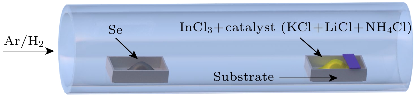
图 1 CVD 法制备二维α-In2Se3材料的示意图
Fig. 1. Schematic diagram of the CVD synthesis of two-dimensional α-In2Se3 material.
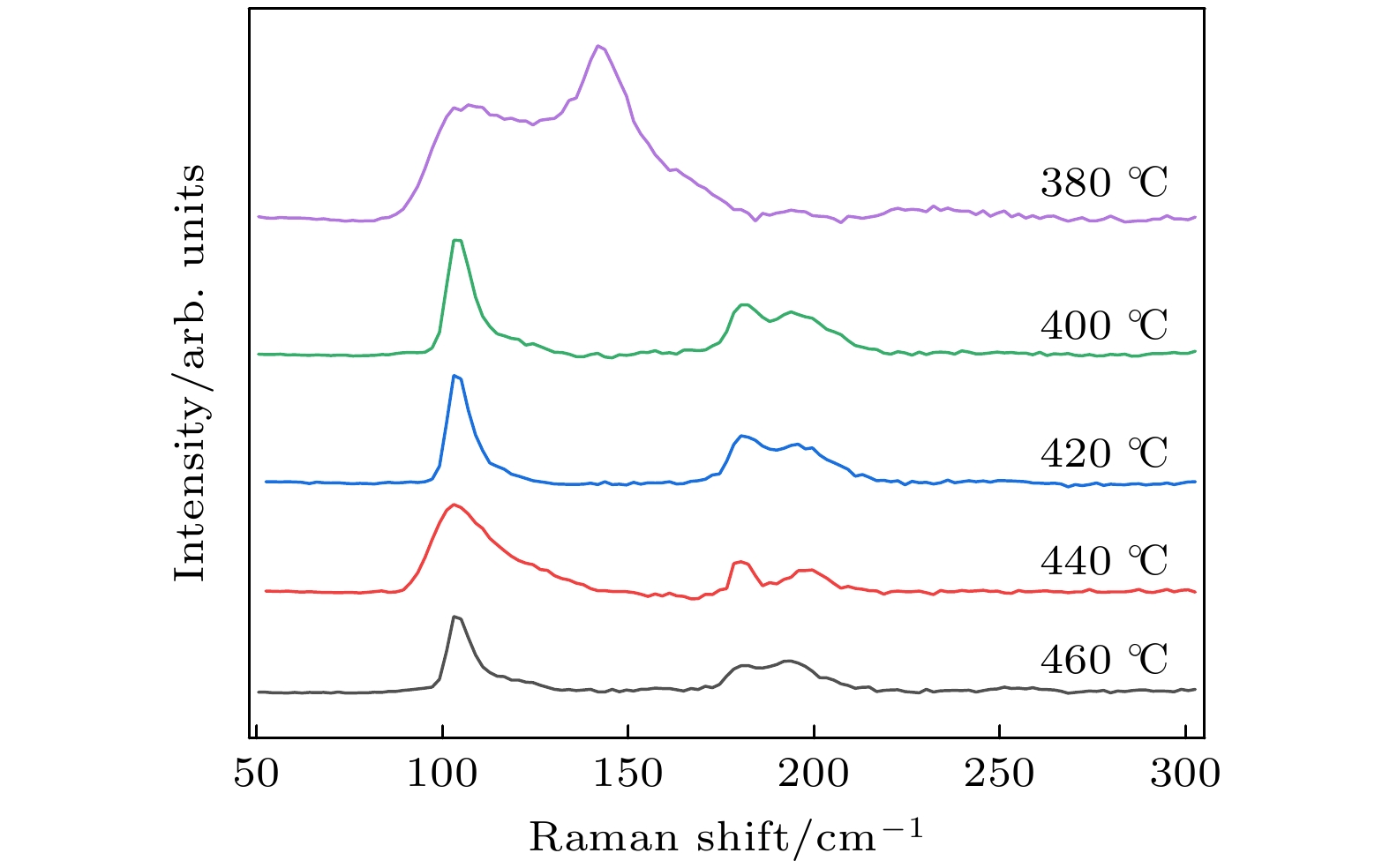
图 2 不同生长温度下制备得到的α-In2Se3的拉曼光谱图
Fig. 2. Raman spectra of α-In2Se3 synthesized at different growth temperatures.
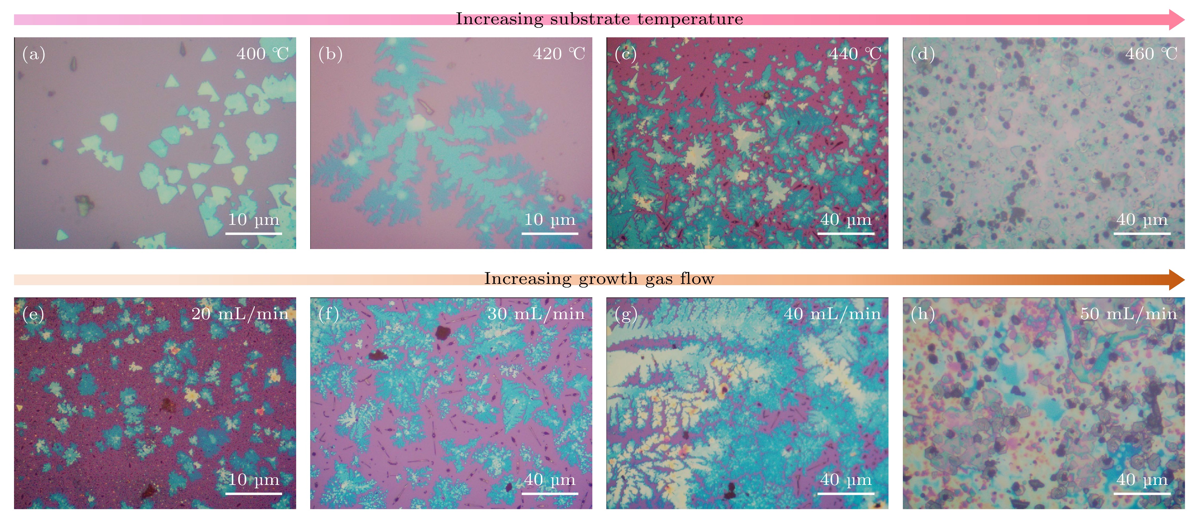
图 3 (a)—(d) 在20 mL/min (标准状况)气体流量、不同生长温度下, 生长的In2Se3薄片光学显微图; (e)—(h) 在440 ℃、不同气体流量(标准状况)下, 生长的In2Se3薄片光学显微图
Fig. 3. (a)–(d) Optical images of In2Se3 flakes grown at gas flow rate of 20 mL/min (standard condition) and different growth temperature; (e)–(h) optical images of In2Se3 flakes grown at 440 ℃ and different gas flow rate (standard condition).

图 4 (a)—(d) 各个温度生长的In2Se3的SEM图; (e) 各元素百分比含量
Fig. 4. (a)–(d) SEM images of In2Se3 grown at various temperatures; (e) percentage content of each element.

图 5 (a) In 3d3/2和In 3d5/2的XPS能谱; (b) Se 3d3/2和Se 3d5/2的XPS能谱; (c) 合成α-In2Se3的XPS能谱; (d) α-In2Se3 AFM图像及对应的高度剖面图
Fig. 5. (a) XPS spectra of In 3d3/2 and In 3d5/2; (b) XPS spectra of Se 3d3/2 and Se 3d5/2; (c) XPS spectrum of synthesized α-In2Se3; (d) AFM image of the α-In2Se3 and corresponding height profile.

图 6 Au/α-In2Se3/Au忆阻器的10个循环周期的I-V特性曲线(插图为器件结构示意图)
Fig. 6. I-V characteristic curves of the Au/α-In2Se3/Au memristor for 10 cycles (inset shows a schematic diagram of the device structure).

图 7 20组重复的相同大小的电脉冲诱导的LTP/LTD行为
Fig. 7. LTP/LTD behavior induced by 20 sets of repetitive identical-sized electrical pulses.
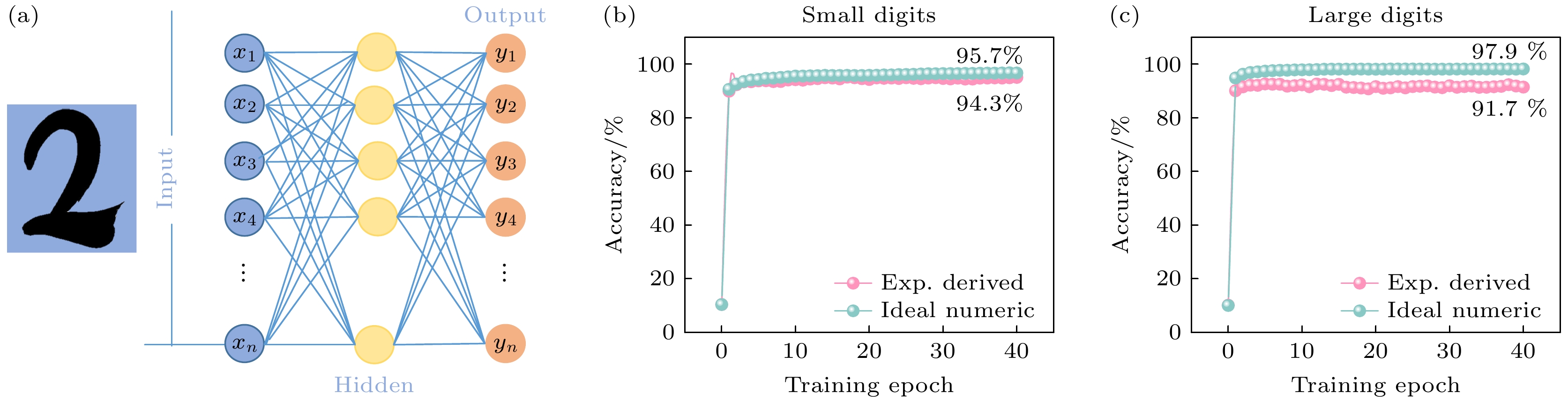
图 8 (a) 3层神经网络ANN示意图; (b) 8×8像素的识别精度; (c) 28×28像素的识别精度
Fig. 8. (a) Schematic structure of three-layer neural network ANN structure; (b) recognition accuracy of 8×8 pixels; (c) recognition accuracy of 28×28 pixels.
表 1 不同条件合成α-In2Se3
Table 1. Synthesis of α-In2Se3 under different conditions.
In源 Se源 催化剂 衬底 文献 In2O3
(650—750 ℃)Se粉(300 ℃) 无 mica [17] In2O3
(680—750 ℃)Se粉(250 ℃) 无 mica [18] In2O3
(700—900 ℃)Se粉 无 mica [19] In2O3
(630 ℃)Se粉(250 ℃) 无 mica [20] In2O3
(850 ℃)Se粉(270 ℃) 无 SiO2/Si [14] In2O3
(550/650 ℃)Se粉(270 ℃) 无 SiO2/Si [21] In2O3
(670 ℃)Se粉(250 ℃) 无 mica [22] In2Se3
(850 ℃)— 无 SiO2/Si [23] In2O3
(660 ℃)Se粉(350 ℃) 无 mica [24] In2O3
(660 ℃)Se粉(300 ℃) 无 mica [25] InCl3
(400—460 ℃)Se粉(300 ℃) KCl/NaCl/
NH4ClSiO2/Si 本工作  下载: 导出CSV
-
[1] Wu J B, Chen H Y, Yang N, Cao J, Yan X D, Liu F X, Sun Q B, Ling X, Guo J, Wang H 2020 Nat. Electron. 3 466
Google Scholar
[2] Wang S Y, Liu L, Gan L R, Chen H W, Hou X, Ding Y, Ma S L, Zhang D W, Zhou P 2021 Nat. Commun. 12 53
Google Scholar
[3] Wang X W, Zhu C, Deng Y, Duan R H, Chen J Q, Zeng Q S, Zhou J D, Fu Q D, You L, Liu S, Edgar J H, Yu P, Liu Z 2021 Nat. Commun. 12 1109
Google Scholar
[4] Dai M J, Wang Z G, Wang F K, Qiu Y F, Zhang J, Xu C Y, Zhai T Y, Cao W W, Fu Y Q, Jia D C, Zhou Y, Hu P A 2019 Nano Lett. 19 5410
Google Scholar
[5] Zhou Y, Wu D, Zhu Y H, Cho Y J, He Q, Yang X, Herrera K, Chu Z D, Han Y, Downer M C, Peng H L, Lai K J 2017 Nano Lett. 17 5508
Google Scholar
[6] Chang K, Liu J W, Lin H C, Wang N, Zhao K, Zhang A M, Jin F, Zhong Y, Hu X P, Duan W H, Zhang Q M, Fu L, Xue Q K, Chen X, Ji S H 2016 Science 353 274
Google Scholar
[7] Li M D, He Y Y, Wang C Y, Io W F, Guo F, Jie W J, Hao J H 2025 Small 2412314
Google Scholar
[8] Si M W, Saha A K, Gao S J, Qiu G, Qin J K, Duan Y Q, Jian J, Niu C, Wang H Y, Wu W Z, Gupta S K, Ye P D 2019 Nat. Electron. 2 580
Google Scholar
[9] Popović S, Čelustka B, Bidjin D 1971 Physica Status Solidi (a) 6 301
Google Scholar
[10] Osamura K, Murakami Y, Tomiie Y 1966 J. Phys. Soc. Jpn. 21 1848
Google Scholar
[11] Ding W J, Zhu J B, Wang Z, Gao Y F, Xiao D, Gu Y, Zhang Z Y, Zhu W G 2017 Nat. Commun. 8 14956
Google Scholar
[12] Cui C J, Hu W J, Yan X X, Addiego C, Gao W P, Wang Y, Wang Z, Li L Z, Cheng Y C, Li P, Zhang X X, Alshareef H N, Wu T, Zhu W G, Pan X Q, Li L J 2018 Nano Lett. 18 1253
Google Scholar
[13] Han W, Zheng X D, Yang K, Tsang C S, Zheng F Y, Wong L W, Lai K H, Yang T F, Wei Q, Li M J, Io W F, Guo F, Cai Y, Wang N, Hao J H, Lau S P, Lee C S, Ly T H, Yang M, Zhao J 2023 Nat. Nanotechnol. 18 55
Google Scholar
[14] Liu L X, Dong J Y, Huang J Q, Nie A M, Zhai K, Xiang J Y, Wang B C, Wen F S, Mu C P, Zhao Z S, Gong Y J, Tian Y J, Liu Z Y 2019 Chem. Mater. 31 10143
Google Scholar
[15] Li J, Wang X T, Ma Y, Han W, Li K X, Li J T, Wu Y, Zhao Y H, Yan T, Liu X, Shi H L, Chen X Q, Zhang Y Z 2025 ACS Nano 19 13220
Google Scholar
[16] Jiang Y X, Ning X K, Liu R H, Song K P, Ali S, Deng H Y, Li Y Z, Huang B H, Qiu J H, Zhu X F, Fan Z, Li Q K, Qin C B, Xue F, Yang T, Li B, Liu G, Hu W J, Li L J, Zhang Z D 2025 Nat. Commun. 16 7364
Google Scholar
[17] Xu L, Wu Z H, Han Y T, Wang M Z, Li J, Chen C, Wang L, Yuan Y K, Shi L, Redwing J M, Zhang X T 2025 Nano Lett. 25 8423
Google Scholar
[18] He Q M, Tang Z Y, Dai M Z, Shan H L, Yang H, Zhang Y, Luo X 2023 Nano Lett. 23 3098
Google Scholar
[19] Zhou S Y, Liao L C, Chen J H, Yu Y Y, Lü Z Q, Yang M, Yao B W, Zhang S, Peng G, Huang Z Y, Liu Y Y, Qi X, Wang G 2023 ACS Appl. Mater. Interfaces 15 23613
Google Scholar
[20] Mukherjee S, Dutta D, Mohapatra P K, Dezanashvili L, Ismach A, Koren E 2020 ACS Nano 14 17543
Google Scholar
[21] Zhang Z, Shi L, Wang B, Qu J Y, Wang X L, Wang T, Jiang Q T, Xue W H, Xu X H 2025 Chin. Chem. Lett. 36 109687
Google Scholar
[22] He Q M, Jiang B, Ma J Y, Chen W J, Luo X, Zheng Y 2025 Small Methods 9 2401549
Google Scholar
[23] Zhou J D, Zeng Q S, Lü D H, Sun L F, Niu L, Fu W, Liu F C, Shen Z X, Jin C H, Liu Z 2015 Nano Lett. 15 6400
Google Scholar
[24] Feng W, Zheng W, Gao F, Chen X S, Liu G B, Hasan T, Cao W W, Hu P A 2016 Chem. Mater. 28 4278
Google Scholar
[25] Io W F, Yuan S, Pang S Y, Wong L W, Zhao J, Hao J 2020 Nano Res. 13 1897
Google Scholar
[26] Sangster J, Pelton A D 1987 J. Phys. Chem. Ref. Data 16 509
Google Scholar
[27] Li Z L, Zhou J Y, Wang Z P, Gu J H, Zhang Y W, Wei Y X 2012 Adv. Mater. Res. 567 41
Google Scholar
[28] Won Y S, Kim Y S, Kryliouk O, Anderson T 2008 Physica Status Solidi c 5 1633
Google Scholar
[29] Yang K M, Wang J P, Wu L, Yan Y F, Tang X, Gan W, Li L, Li Y, Han H, Li H 2023 Results Phys. 51 106643
Google Scholar
[30] Kim J H, Kim S H, Yu H Y 2024 Small 20 2405459
Google Scholar
[31] Wang D, Yin J, Li Y, Li H, Wang M, Guo F, Jie W, Song F, Hao J 2025 Aggregate 6 e70099
Google Scholar
[32] Zhong Y N, Wang T, Gao X, Xu J L, Wang S D 2018 Adv. Funct. Mater. 28 1800854
Google Scholar
[33] Guo F, Song M L, Wong M C, Ding R, Io W F, Pang S Y, Jie W J, Hao J H 2022 Adv. Funct. Mater. 32 2108014
Google Scholar


 下载:
下载:


计量
- 文章访问数: 1481
- PDF下载量: 43
- 被引次数: 0
