


-
作为二维半导体过渡金属硫族化物中的典型代表性材料, MoS2具有带隙可调谐特性等优异物理特性. 因此, MoS2莫尔超晶格是研究凝聚态电子输运问题和设计光电器件的理想体系. 另一方面, 层间电导的测量是研究莫尔超晶格层间耦合作用的重要手段. 为了阐明带隙可调谐等特性对莫尔超晶格层间电导的影响, 有必要对MoS2莫尔超晶格的层间电导特性加以研究. 本文利用衍射物理中的光学方法, 构建了MoS2莫尔超晶格体系的隧穿理论. 在该理论中, 将MoS2莫尔超晶格中电子的隧穿视作电子波为周期性光栅所散射. 利用该理论研究了MoS2莫尔超晶格的层间电导特性. 研究结果表明: 由于衍射效应, 界面处隧穿电子波存在两个分波均与界面势产生共振, 所以层间电导随扭转角的变化呈现双峰结构. 进一步还研究了隧穿层和金属电极对层间电导的影响: 上层和下层MoS2晶格厚度分别影响层间电导的峰和背景; 界面势强度的增大可以增强隧穿电子的相干性; 金属电极化学势主要影响MoS2莫尔超晶格层间电导峰的特性, 且相比于石墨莫尔超晶格, 影响更为显著.MoS2, as a typical material of two-dimensional semiconductor transition metal chalcogenides, has excellent physical properties such as tunable band gap. Therefore, MoS2 moiré superlattice is an ideal system for investigating the electron transport in condensed matter and the design of optoelectronic devices. On the other hand, interlayer conductance serves as a significant indicator for analyzing coupling effects in moiré superlattice. Here, in order to clarify the influence of tunable band gap on the interlayer conductance, we develop a tunneling theory for calculating the interlayer conductance of MoS2 moiré superlattices by using optical methods in diffraction physics. In this theory, the electron tunneling can be considered as the diffraction of electron waves by the periodic gratings. Accordingly, the influences of the periodicity of MoS2 moiré superlattices and the coherence of the tunneling electrons can be well included in the theory. In addition, the effect of the tunable band gap of MoS2 is taken into account. According to the theory, we investigate the properties of the interlayer conductance of MoS2 moiré superlattice. The theoretical results show that due to the diffraction effect, there exist two partial waves of the tunneling electron at the interface, which can resonate with the interface potential. Accordingly, the interlayer conductance curves exhibit a double-peak structure. Furthermore, we analyze the influences of the tunneling layer and the metal electrodes on the interlayer conductance: the thickness of the upper MoS2 lattice affects the peak and the lower one primarily influences the background. The coherence of tunneling electrons will be enhanced when the parameter of interface potential strength increases. The chemical potential of the metal electrode mainly affects the properties of the peak, and the influence is more significant than that in graphite moiré superlattice.

-
Keywords:
- MoS2 moiré superlattice /
- tunneling conductance /
- diffraction physics /
- twistronics
[1] Cao Y, Fatemi V, Fang S, Watanabe K, Taniguchi T, Kaxiras E, Jarillo-Herrero P 2018 Nature 556 43
 Google Scholar
[2] Naik M H, Jain M 2018 Phys. Rev. Lett. 121 266401
Google Scholar
[3] 李听昕 2022 71 127309
Google Scholar
Li T X 2022 Acta Phys. Sin. 71 127309
Google Scholar
[4] Seyler K L, Rivera P, Yu H, Wilson N P, Ray E L, Mandrus D G, Yan J, Yao W, Xu X 2019 Nature 567 66
Google Scholar
[5] Wang Q H, Kalantar-Zadeh K, Kis A, Coleman J N, Strano M S 2012 Nat. Nanotechnol. 7 699
Google Scholar
[6] Tran K, Moody G, Wu F, Lu X, Choi J, Kim K, Rai A, Sanchez D A, Quan J, Singh A, Embley J, Zepeda A, Campbell M, Autry T, Taniguchi T, Watanabe K, Lu N, Banerjee S K, Silverman K L, Kim S, Tutuc E, Yang L, MacDonald A H, Li X 2019 Nature 567 71
Google Scholar
[7] Mak K F, Lee C, Hone J, Shan J, Heinz T F 2010 Phys. Rev. Lett. 105 136805
Google Scholar
[8] Radisavljevic B, Radenovic A, Brivio J, Giacometti V, Kis A 2011 Nat. Nanotechnol. 6 147
Google Scholar
[9] Splendiani A, Sun L, Zhang Y, Li T, Kim J, Chim C Y, Galli G, Wang F 2010 Nano Lett. 10 1271
Google Scholar
[10] Liu K, Zhang L, Cao T, Jin C, Qiu D, Zhou Q, Zettl A, Yang P, Louie S G, Wang F 2014 Nat. Commun. 5 4966
Google Scholar
[11] Liao M, Wei Z, Du L, Wang Q, Tang J, Yu H, Wu F, Zhao J, Xu X, Han B, Liu K, Gao P, Polcar T, Sun Z, Shi D, Yang R, Zhang G 2020 Nat. Commun. 11 2153
Google Scholar
[12] Xu M, Ji H, Zheng L, Li W, Wang J, Wang H, Luo L, Lu Q, Gan X, Liu Z, Wang X, Huang W 2024 Nat. Commun. 15 562
Google Scholar
[13] Zhou J, Huang H, Zhao Z, Dou Z, Zhou L, Zhang T, Huang Z, Feng Y, Shi D, Liu N, Yang J, Nie J C, Wang Q, Dong J, Liu Y, Dou R, Xue Q 2024 Adv. Mater. 36 2408227
Google Scholar
[14] Garcia-Ruiz A, Liu M H 2024 Nano Lett. 24 16317
Google Scholar
[15] Yang M M, Cong R D, Wu C L, Zhang Y, Gao Q, Hu X W, Zhang Y F, Tan L, Liang B L, Zhao X H, Li X L 2024 Surf. Interfaces 52 104790
Google Scholar
[16] Li H, Wei X, Wu G, Gao S, Chen Q, Peng L M 2018 Ultramicroscopy 193 90
Google Scholar
[17] Koren E, Leven I, Lörtscher E, Knoll A, Hod O, Duerig U 2016 Nat. Nanotechnol. 11 752
Google Scholar
[18] Chari T, Ribeiro-Palau R, Dean C R, Shepard K 2016 Nano Lett. 16 4477
Google Scholar
[19] Yu Z, Song A, Sun L, Li Y, Gao L, Peng H, Ma T, Liu Z, Luo J 2020 Small 16 1902844
Google Scholar
[20] Zhang S, Song A, Chen L, Jiang C, Chen C, Gao L, Hou Y, Liu L, Ma T, Wang H, Feng X Q, Li Q 2020 Sci. Adv. 6 eabc5555
Google Scholar
[21] Inbar A, Birkbeck J, Xiao J, Taniguchi T, Watanabe K, Yan B, Oreg Y, Stern A, Berg E, Ilani S 2023 Nature 614 682
Google Scholar
[22] Birkbeck J, Xiao J, Inbar A, Taniguchi T, Watanabe K, Berg E, Glazman L, Guinea F, Von Oppen F, Ilani S 2025 Nature 641 345
Google Scholar
[23] Fang H, Xiao M 2021 ACS Appl. Electron. Mater. 3 2543
Google Scholar
[24] Tao Y Z, Liu C, Xiao M W, Fang H N 2024 Chin. Phys. B 33 107301
Google Scholar
[25] Liao M, Wu Z W, Du L, Zhang T, Wei Z, Zhu J, Yu H, Tang J, Gu L, Xing Y 2018 Nat. Commun. 9 4068
Google Scholar
[26] Molinàs-Mata P 1996 Phys. Rev. A 54 2060
Google Scholar
[27] Kočinac S L S, Milanović V 2008 Phys. Lett. A 372 191
Google Scholar
[28] Kittle C 2005 Introduction of Solid State Physics (New York: John Wiley & Sons, Inc) p229
[29] Cowley J M 1995 Diffraction Physics (Amsterdam: Elsevier) p177
[30] Fang H, Xiao M, Rui W, Du J, Tao Z 2016 Sci. Rep. 6 24300
Google Scholar
[31] Ataca C, Ciraci S 2011 J. Phys. Chem. C 115 13303
Google Scholar
[32] Zhang G, Huang S, Chaves A, Song C, Özçelik V O, Low T, Yan H 2017 Nat. Commun. 8 14071
Google Scholar
-
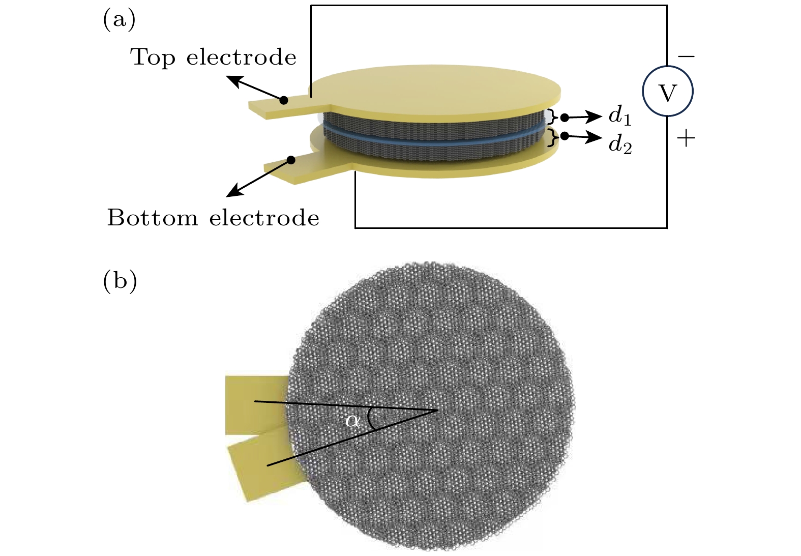
图 1 (a) MoS2莫尔超晶格体系示意图; (b) MoS2莫尔超晶格的俯视图
Fig. 1. (a) Schematic illustration of MoS2 moiré superlattices; (b) top view of MoS2 moiré superlattices.
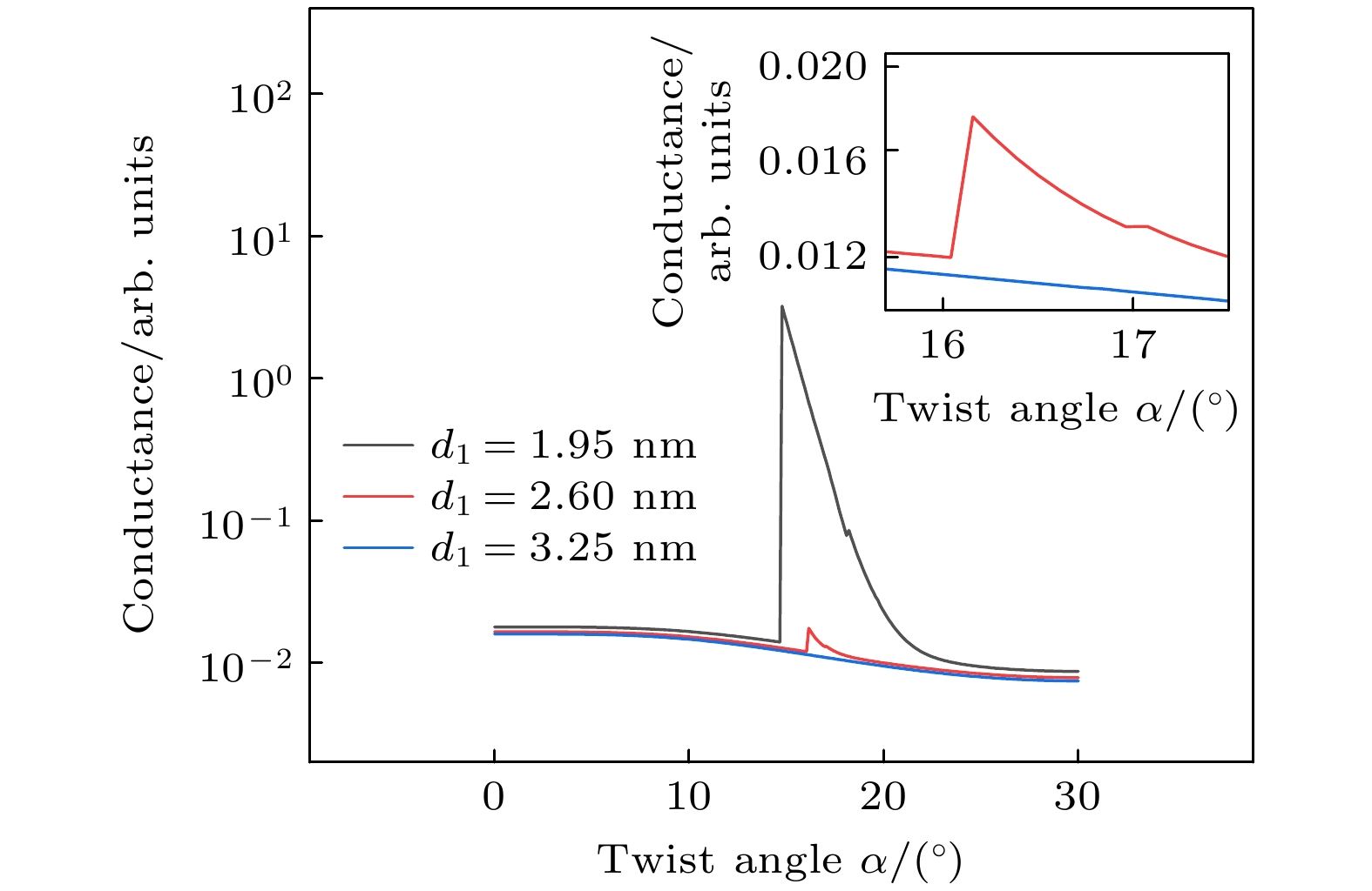
图 2 不同上层厚度下关于扭转角的层间电导曲线, 内插图为d1 = 2.60 nm时电导峰的放大图
Fig. 2. Interlayer conductance curves versus twist angle under different d1, and the inset is the enlarged figure of the peak of d1 = 2.60 nm.
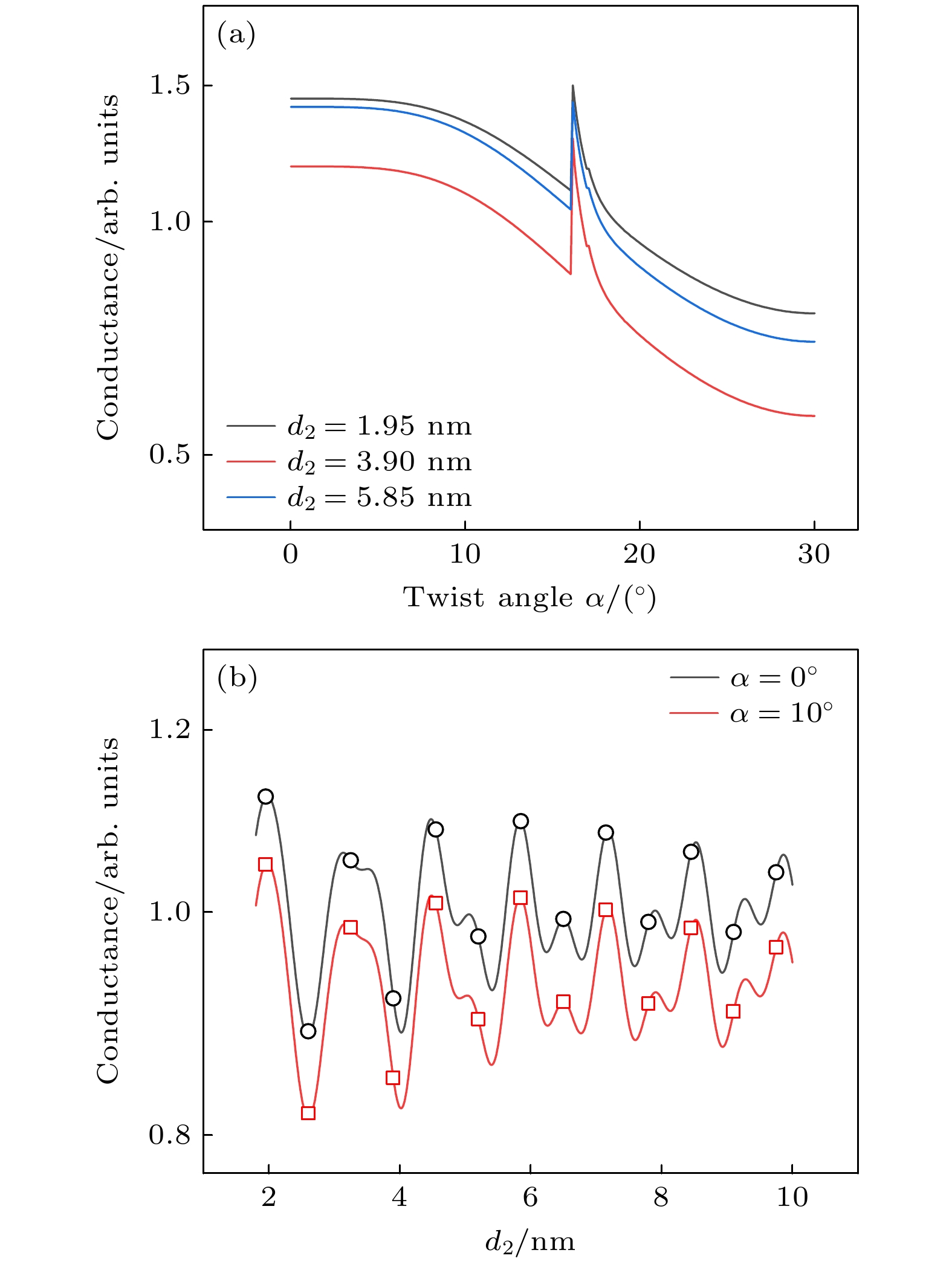
图 3 (a)不同下层厚度下关于扭转角的层间电导曲线; (b)当扭转角α分别为0°和10°时层间电导背景随下层厚度的变化曲线, 其中对应于整数层厚度的数据点为空心符号所标注
Fig. 3. (a) Interlayer conductance curves versus twist angle under different d2; (b) the background as a function of d2 under different twist angles, and the data corresponding to the discrete layers are marked with open symbols.
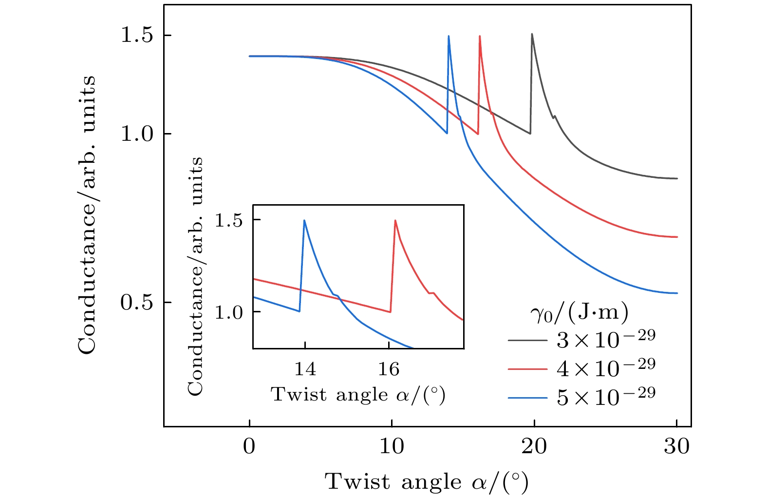
图 4 不同界面势强度参数下关于扭转角的层间电导曲线, 内插图为γ0 = 4×10–29 J·m和γ0 = 5×10–29 J·m时电导峰的放大图
Fig. 4. Interlayer conductance curves versus twist angle under different γ0, and the inset is the enlarged figure of the peaks of γ0 = 4×10–29 J·m and γ0 = 5×10–29 J·m.
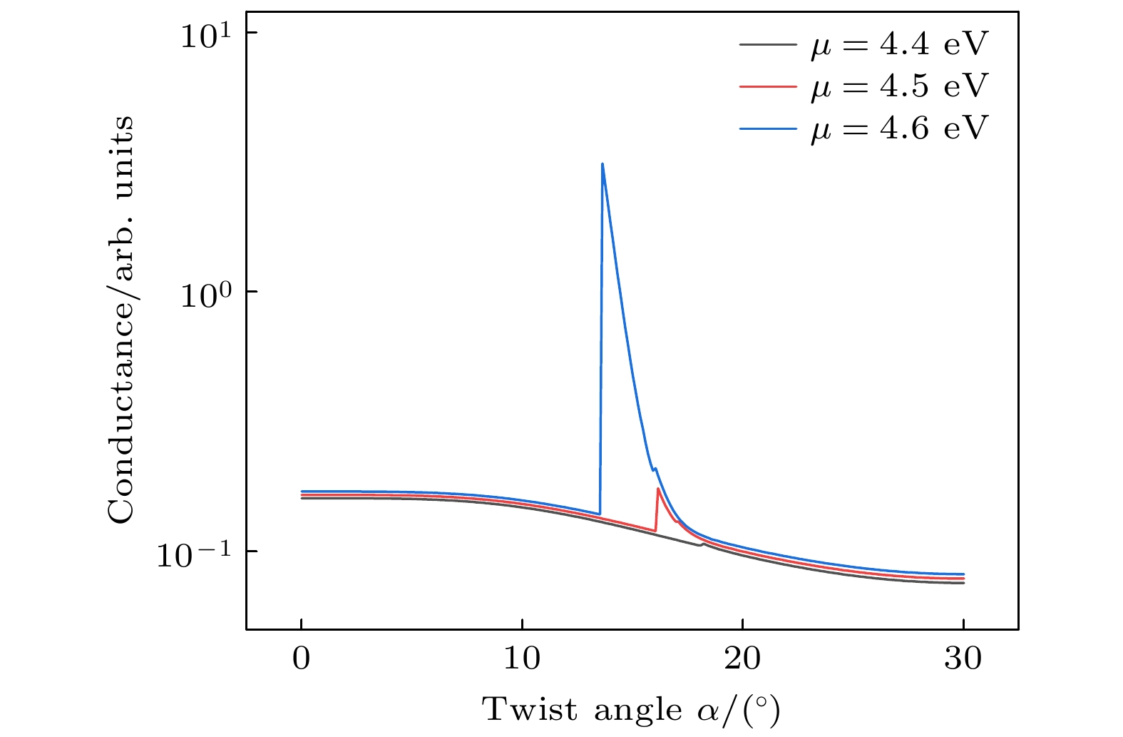
图 5 不同化学势μ下关于扭转角的层间电导曲线
Fig. 5. Interlayer conductance curves versus twist angle under different μ.
-
[1] Cao Y, Fatemi V, Fang S, Watanabe K, Taniguchi T, Kaxiras E, Jarillo-Herrero P 2018 Nature 556 43
Google Scholar
[2] Naik M H, Jain M 2018 Phys. Rev. Lett. 121 266401
Google Scholar
[3] 李听昕 2022 71 127309
Google Scholar
Li T X 2022 Acta Phys. Sin. 71 127309
Google Scholar
[4] Seyler K L, Rivera P, Yu H, Wilson N P, Ray E L, Mandrus D G, Yan J, Yao W, Xu X 2019 Nature 567 66
Google Scholar
[5] Wang Q H, Kalantar-Zadeh K, Kis A, Coleman J N, Strano M S 2012 Nat. Nanotechnol. 7 699
Google Scholar
[6] Tran K, Moody G, Wu F, Lu X, Choi J, Kim K, Rai A, Sanchez D A, Quan J, Singh A, Embley J, Zepeda A, Campbell M, Autry T, Taniguchi T, Watanabe K, Lu N, Banerjee S K, Silverman K L, Kim S, Tutuc E, Yang L, MacDonald A H, Li X 2019 Nature 567 71
Google Scholar
[7] Mak K F, Lee C, Hone J, Shan J, Heinz T F 2010 Phys. Rev. Lett. 105 136805
Google Scholar
[8] Radisavljevic B, Radenovic A, Brivio J, Giacometti V, Kis A 2011 Nat. Nanotechnol. 6 147
Google Scholar
[9] Splendiani A, Sun L, Zhang Y, Li T, Kim J, Chim C Y, Galli G, Wang F 2010 Nano Lett. 10 1271
Google Scholar
[10] Liu K, Zhang L, Cao T, Jin C, Qiu D, Zhou Q, Zettl A, Yang P, Louie S G, Wang F 2014 Nat. Commun. 5 4966
Google Scholar
[11] Liao M, Wei Z, Du L, Wang Q, Tang J, Yu H, Wu F, Zhao J, Xu X, Han B, Liu K, Gao P, Polcar T, Sun Z, Shi D, Yang R, Zhang G 2020 Nat. Commun. 11 2153
Google Scholar
[12] Xu M, Ji H, Zheng L, Li W, Wang J, Wang H, Luo L, Lu Q, Gan X, Liu Z, Wang X, Huang W 2024 Nat. Commun. 15 562
Google Scholar
[13] Zhou J, Huang H, Zhao Z, Dou Z, Zhou L, Zhang T, Huang Z, Feng Y, Shi D, Liu N, Yang J, Nie J C, Wang Q, Dong J, Liu Y, Dou R, Xue Q 2024 Adv. Mater. 36 2408227
Google Scholar
[14] Garcia-Ruiz A, Liu M H 2024 Nano Lett. 24 16317
Google Scholar
[15] Yang M M, Cong R D, Wu C L, Zhang Y, Gao Q, Hu X W, Zhang Y F, Tan L, Liang B L, Zhao X H, Li X L 2024 Surf. Interfaces 52 104790
Google Scholar
[16] Li H, Wei X, Wu G, Gao S, Chen Q, Peng L M 2018 Ultramicroscopy 193 90
Google Scholar
[17] Koren E, Leven I, Lörtscher E, Knoll A, Hod O, Duerig U 2016 Nat. Nanotechnol. 11 752
Google Scholar
[18] Chari T, Ribeiro-Palau R, Dean C R, Shepard K 2016 Nano Lett. 16 4477
Google Scholar
[19] Yu Z, Song A, Sun L, Li Y, Gao L, Peng H, Ma T, Liu Z, Luo J 2020 Small 16 1902844
Google Scholar
[20] Zhang S, Song A, Chen L, Jiang C, Chen C, Gao L, Hou Y, Liu L, Ma T, Wang H, Feng X Q, Li Q 2020 Sci. Adv. 6 eabc5555
Google Scholar
[21] Inbar A, Birkbeck J, Xiao J, Taniguchi T, Watanabe K, Yan B, Oreg Y, Stern A, Berg E, Ilani S 2023 Nature 614 682
Google Scholar
[22] Birkbeck J, Xiao J, Inbar A, Taniguchi T, Watanabe K, Berg E, Glazman L, Guinea F, Von Oppen F, Ilani S 2025 Nature 641 345
Google Scholar
[23] Fang H, Xiao M 2021 ACS Appl. Electron. Mater. 3 2543
Google Scholar
[24] Tao Y Z, Liu C, Xiao M W, Fang H N 2024 Chin. Phys. B 33 107301
Google Scholar
[25] Liao M, Wu Z W, Du L, Zhang T, Wei Z, Zhu J, Yu H, Tang J, Gu L, Xing Y 2018 Nat. Commun. 9 4068
Google Scholar
[26] Molinàs-Mata P 1996 Phys. Rev. A 54 2060
Google Scholar
[27] Kočinac S L S, Milanović V 2008 Phys. Lett. A 372 191
Google Scholar
[28] Kittle C 2005 Introduction of Solid State Physics (New York: John Wiley & Sons, Inc) p229
[29] Cowley J M 1995 Diffraction Physics (Amsterdam: Elsevier) p177
[30] Fang H, Xiao M, Rui W, Du J, Tao Z 2016 Sci. Rep. 6 24300
Google Scholar
[31] Ataca C, Ciraci S 2011 J. Phys. Chem. C 115 13303
Google Scholar
[32] Zhang G, Huang S, Chaves A, Song C, Özçelik V O, Low T, Yan H 2017 Nat. Commun. 8 14071
Google Scholar


 下载:
下载:


计量
- 文章访问数: 405
- PDF下载量: 6
- 被引次数: 0
