


-
一般认为拓扑绝缘体对非磁性缺陷是高度免疫的, 但是在器件应用的介观尺度上还缺乏验证. 本文以SiSnF2单层条带为例, 研究了不同缺陷浓度和尺寸对拓扑绝缘体电子输运的影响. 第一性原理计算发现, SiSnF2在大于2%的拉伸应变下转变为拓扑绝缘体. 用遗传算法拟合了有效紧束缚模型的参数, 计算了拓扑绝缘体SiSnF2条带输运性质, 发现边缘态也可能被随机空位缺陷破坏. 对于长18.8 nm、宽8.2 nm的条带, 在没有缺陷时, 电流集中在条带边缘, 电导为拓扑边缘态的理想值2e2/h. 当缺陷浓度为1%时, 边缘电流已被明显扰动, 但背散射仍受到有效抑制, 电流绕过缺陷向前传输. 当浓度为5%时, 边缘电子经散射深入条带内部, 与另一边缘发生散射, 破坏了拓扑边缘态, 使电导降为0.6e2/h. 因此, 缺陷导致的由拓扑绝缘体到普通绝缘体的转变是渐变而不是突变. 研究发现了明显的输运量子尺寸效应, 增大条带宽度可减小边缘间电子散射, 增强拓扑边缘态的稳定性; 而增大长度会增大电子的局域性和边缘间电子散射, 降低拓扑边缘态的稳定性.It is generally believed that topological insulators are highly immune to non-magnetic defects, but there is still a lack of verification on a mesoscopic scale of device applications. We take SiSnF2 monolayer ribbons as an illustration to study the effects of defects and sizes on the electron transport in topological insulators. First-principles calculations show that SiSnF2 is transformed into a topological insulator under a tensile strain greater than 2%. The data of an effective tight-binding model are obtained by using a genetic algorithm to calculate the transport properties of the topological insulator SiSnF2 ribbons, and it is found that edge states can also be disrupted by random vacancy defects. For a ribbon with a length of 18.8 nm and a width of 8.2 nm, when it has no defects, the current is concentrated at its edge, and its conductance is an ideal value of the topological edge state, 2e2/h. When the defect concentration is 1%, the edge current is appreciably disturbed, but the backscattering is still effectively suppressed, and the current bypasses the defect and still goes forward. When the concentration is 5%, the edge electrons are scattered deep into the ribbon and scattered with the opposite edge, destroying the topological edge state and reducing the conductance to 0.6e2/h. Therefore, the transformation from topological to normal insulator caused by defects happens gradually rather than suddenly. Found in this study is an obvious transport quantum size effect, i.e. increasing the ribbon width can reduce electron scattering between edges and enhance the stability of topological edge states; while increasing the length will increase electron localization and electron scattering between edges, reducing the stability of topological edge states.
-
Keywords:
- topological insulators /
- electron transport /
- defects /
- quantum size effects
[1] Kane C L, Mele E J 2005 Phys. Rev. Lett. 95 226801
 Google Scholar
[2] Kane C L, Mele E J 2005 Phys. Rev. Lett. 95 146802
Google Scholar
[3] Moore J E 2010 Nature 464 194
Google Scholar
[4] Hasan M Z, Kane C L 2010 Rev. Mod. Phys. 82 3045
Google Scholar
[5] Qi X L, Zhang S C 2011 Rev. Mod. Phys. 83 1057
Google Scholar
[6] Aslani Z, Sisakht E T, Fazileh F, Ghorbanfekr-Kalashami H, Peeters F M 2019 Phys. Rev. B 99 115421
Google Scholar
[7] Ezawa M 2015 J. Phys. Soc. Jpn. 84 121003
Google Scholar
[8] Cheng S G, Liu H, Jiang H, Sun Q F, Xie X C 2018 Phys. Rev. Lett. 121 156801
Google Scholar
[9] Zhang H, Liu C X, Qi X L, Dai X, Fang Z, Zhang S C 2009 Nat. Phys. 5 438
Google Scholar
[10] Konig M, Wiedmann S, Brune C, Roth A, Buhmann H, Molenkamp L W, Qi X L, Zhang S C 2007 Science 318 766
Google Scholar
[11] Knez I, Du R R, Sullivan G 2011 Phys. Rev. Lett. 107 136603
Google Scholar
[12] Chuang F C, Yao L Z, Huang Z Q, Liu Y T, Hsu C H, Das T, Lin H, Bansil A 2014 Nano Lett. 14 2505
Google Scholar
[13] Ma Y, Kou L, Du A, Heine T 2015 Nano Res. 8 3412
Google Scholar
[14] Teshome T, Datta A 2018 ACS Omega 3 1
Google Scholar
[15] Liu W, Luo C, Peng X 2024 J. Phys. Condens. Mat. 36 165401
Google Scholar
[16] Zhang S J, Ji W X, Zhang C W, Li S S, Li P, Ren M J, Wang P J 2016 RSC Adv. 6 79452
Google Scholar
[17] Li S S, Ji W X, Zhang C W, Li P, Wang P J 2016 J. Mater. Chem. C 4 2243
Google Scholar
[18] Şahin H, Cahangirov S, Topsakal M, Bekaroglu E, Akturk E, Senger R T, Ciraci S 2009 Phys. Rev. B 80 155453
Google Scholar
[19] Wang Y, Ding Y 2016 Appl. Surf. Sci. 382 1
Google Scholar
[20] Li T C, Lu S P 2008 Phys. Rev. B 77 085408
Google Scholar
[21] Li Y Q, Liu Y Y, Zhang Q, Zhao C Z, Sun J L, Li Y H, Liu Y, Ning P F, Liu Y, Xing H Y 2025 Physica B 698 416757
Google Scholar
[22] Pineda-Medina R, Vinck-Posada H, Herrera W J 2025 Solid State Commun. 395 115729
Google Scholar
[23] Lü X L, Xie H 2022 New J. Phys. 24 033010
Google Scholar
[24] Li S, Liu T, Liu C, Wang Y, Lu H Z, Xie X 2024 Nat. Sci. Rev. 11 296
Google Scholar
[25] Huang L, He L, Zhang W X, Zhang H Z, Liu D N, Feng X, Liu F, Cui K Y, Huang Y D, Zhang W, Zhang X D 2024 Nat. Commun. 15 1647
Google Scholar
[26] 刘畅, 王亚愚 2023 72 177301
Google Scholar
Liu C, Wang Y Y 2023 Acta Phys. Sin. 72 177301
Google Scholar
[27] Slater J C, Koster G F 1954 Phys. Rev. 94 1498
Google Scholar
[28] Kresse G, Furthmüller J 1996 Comp. Mater. Sci. 6 15
Google Scholar
[29] Kresse G, Furthmüller J 1996 Phys. Rev. B 54 11169
Google Scholar
[30] Perdew J P, Burke K, Ernzerhof M 1996 Phys. Rev. Lett. 77 3865
Google Scholar
[31] Monkhorst H J, Pack J D 1976 Phys. Rev. B 13 5188
Google Scholar
[32] Moldovan D 2016 Pybinding v0.8.0: A Python Package for Tight-binding Calculations (Zenodo
[33] Groth C W, Wimmer M, Akhmerov A R, Waintal X 2014 New J. Phys. 16 063065
Google Scholar
[34] Imry Y, Landauer R 1999 Rev. Mod. Phys. 71 S306
Google Scholar
[35] Landauer R 1957 IBM J. Res. Develop. 1 223
Google Scholar
[36] Büttiker M 1986 Phys. Rev. Lett. 57 1761
Google Scholar
[37] Hsu H C, Kleftogiannis I, Guo G Y, Gopar V A 2018 J. Phys. Soc. Jpn. 87 034701
Google Scholar
[38] Ezawa M 2012 New J. Phys. 14 033003
Google Scholar
[39] Rezaei M, Sisakht E T, Fazileh F, Aslani Z, Peeters F M 2017 Phys. Rev. B 96 085441
Google Scholar
[40] Deylgat E, Tiwari S, Vandenberghe W G, Sorée B 2022 J. Appl. Phys. 131 235101
Google Scholar
[41] Vannucci L, Olsen T, Thygesen K S 2020 Phys. Rev. B 101 155404
Google Scholar
-
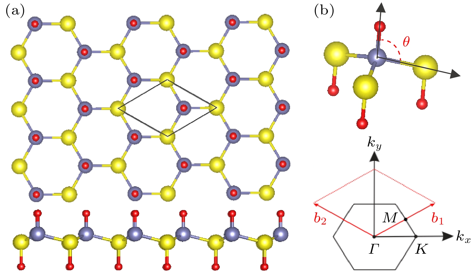
图 1 (a) SiSnF2单层的俯视图(上)和正视图(下), 灰色、黄色和红色的原子分别是Si, Sn和F原子; (b) Si—Sn键与法线的夹角θ (上)和六边形布里渊区(下), Γ, K和M是高对称点
Fig. 1. (a) Top view (top) and side view (bottom) of the monolayer SiSnF2. The gray, yellow, and red spheres represent the Si, Sn, and F atoms, respectively. (b) The angle between the Si—Sn bond and the normal θ (top) and the hexagonal Brillouin zone (bottom) where Γ, K, and M are high symmetry points.
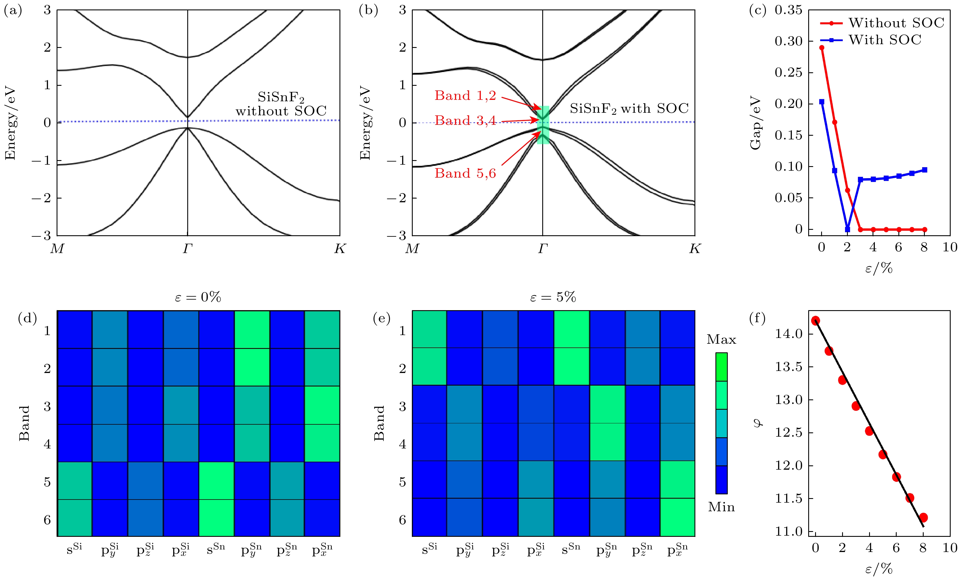
图 2 (a), (b) 分别是SiSnF2不考虑和考虑SOC时的能带; (c) 不同拉伸应变下的带隙; (d), (e) 是图(b)中所标注的费米能级附近6条能带, 在拉伸应变ε= 0%和5%时在Γ点处的轨道成分图; (f) 屈曲角度随拉伸应变的变化
Fig. 2. (a), (b) Band structures without and with SOC, respectively; (c) the band gap variation with respect to tensile strains; (d), (e) the orbital composition diagrams of the 6 bands, as indicated in panel (b), near the Fermi level at the Γ point under the tensile strains of ε = 0% and 5%, respectively; (f) the buckling angles under different strains.
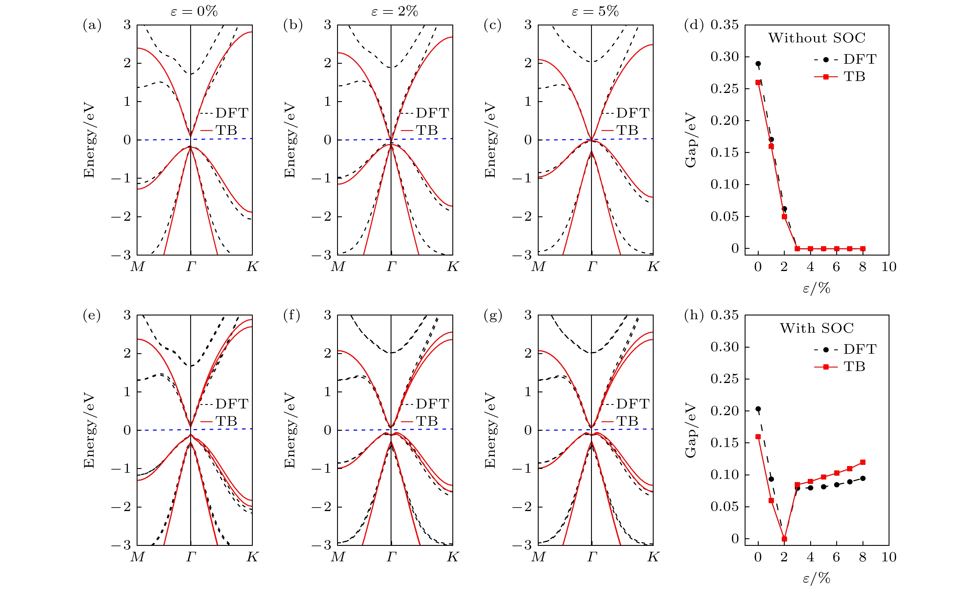
图 3 用表1中S-K参数计算 SiSnF2的紧束缚能带(红色实线)和第一性原理计算的能带(黑色虚线) (a), (b), (c)和(e), (f), (g)分别是不考虑和考虑SOC的情形下, 分别施加0%, 2%和5%应变的能带; (d), (h)是不考虑和考虑SOC时的TB带隙和DFT带隙随应变的变化
Fig. 3. (a), (b), (c) and (e), (f), (g) Energy bands calculated by the tight-binding model (red solid lines) using the S-K parameters in Table 1 and by first-principles calculations (black dashed lines) without and with SOC under 0%, 2%, and 5% strain, respectively; (d), (h) the variations of the TB and DFT band gaps with respect to the strains without and with SOC, respectively.
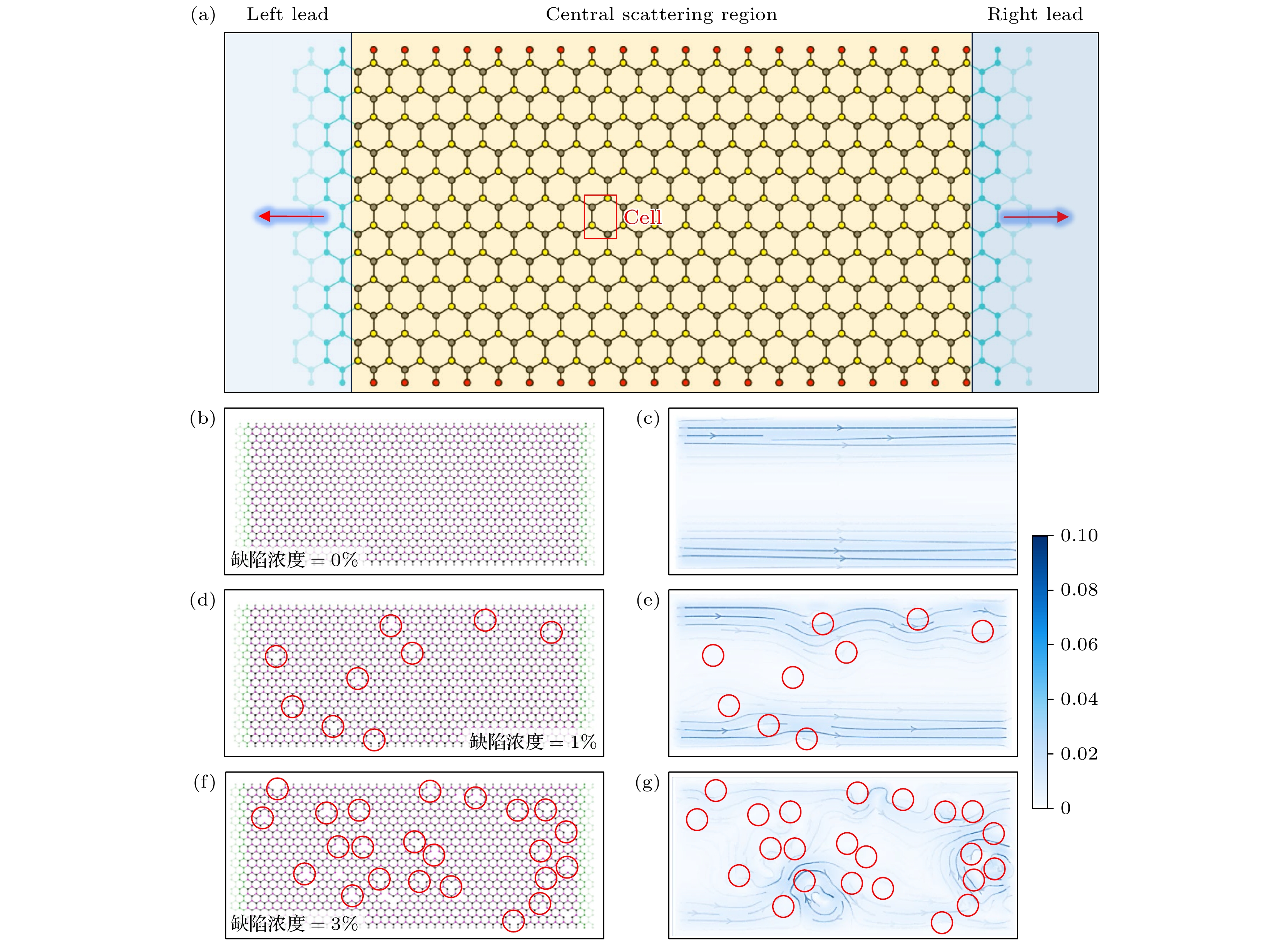
图 4 (a) 用来计算SiSnF2输运的构型, 其中, 中间散射区是SiSnF2锯齿条带, 两端连接由SiSnF2锯齿条带构成的左右电极, 所示红色矩形是条带内部的结构单元; (b), (d), (f)分别是随机缺陷浓度为0%, 1%, 3%时散射区SiSnF2条带的结构图; (c), (e), (g)分别对应图(b), (d), (f)在激发能取E = 0.002 eV时的局域电流分布, 箭头表示局部电流方向, 图中的红色圆圈指示缺陷的位置
Fig. 4. (a) Configuration employed to calculate the transport in SiSnF2: the central scattering region is a SiSnF2 zigzag ribbon, whose two ends are connected to the left and right electrodes made of SiSnF2 zigzag ribbon. The red rectangle indicates the structure unit inside the ribbon. (b), (d), (f) Scattering region with random defects of the concentrations of 0%, 1% and 3%, respectively; (c), (e), (g) the local current distributions corresponding to panel (b), (d), (f), respectively, when excitation energy E = 0.002 eV. The arrows indicate the direction of local current. The red circles in this figure designate the location of the defects.
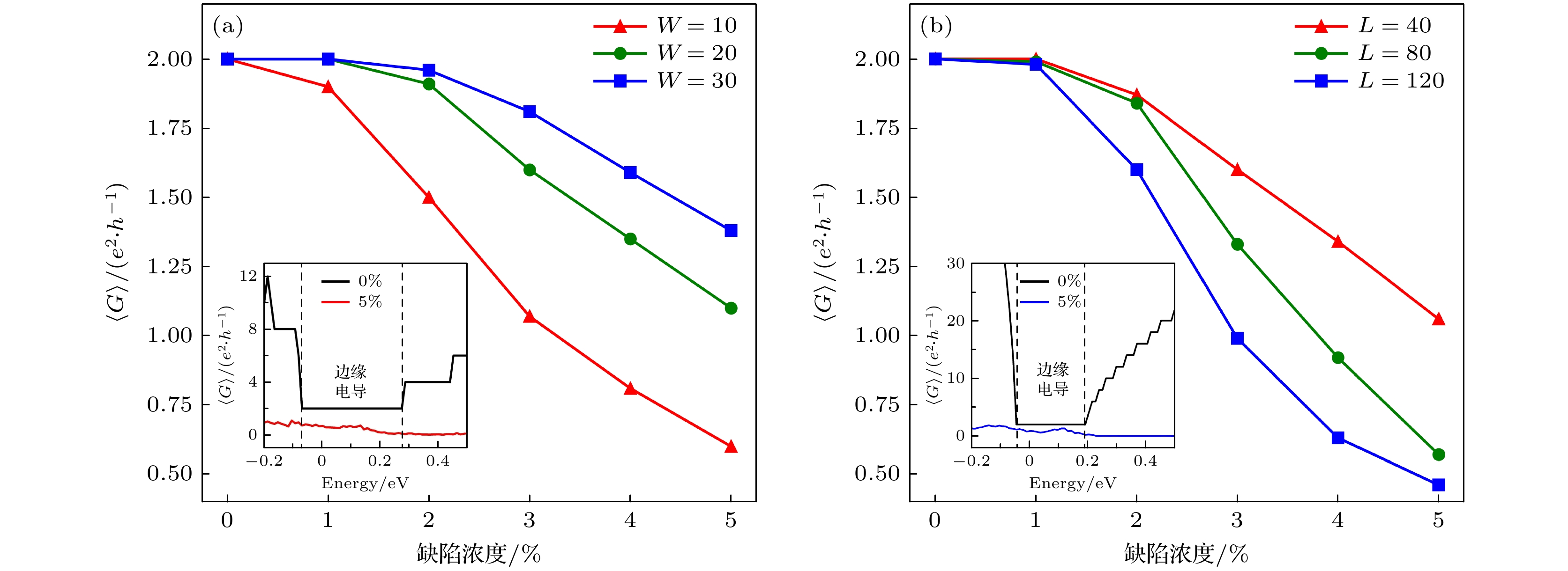
图 5 (a) 固定长度L = 40, 不同宽度的SiSnF2条带的平均电导随缺陷浓度的变化, 插图为长度L = 40, W = 10的条带在缺陷浓0%度和5%情形下, 电导平台的变化; (b) 固定条带宽度W = 40, 不同长度的SiSnF2条带条带的平均电导随缺陷浓度的变化, 插图为长度L = 120, W = 40的条带在缺陷浓度0%和5%情形下, 电导平台的变化; 激发能E 取值为 0.002 eV
Fig. 5. (a) Average conductance versus the defect concentration for SiSnF2 ribbons of different widths with fixed length L = 40. The inset: the conductance plateau for the strip change with length L = 40 and width W = 10 at defect concentrations of 0% and 5%. (b) The average conductance versus the defect concentration for SiSnF2 ribbons of different lengths with fixed width W = 40. The inset: the conductance plateau for the strip change with length L = 120 and width W = 40 at defect concentrations of 0% and 5%. The excitation energy is set to be 0.002 eV.
表 1 用遗传算法拟合DFT能带得到的SiSnF2 S-K参数, 单位是eV
Table 1. The S-K parameters obtained by genetic fitting of the DFT bands of SiSnF2. All parameters are in units of eV.
ssσ spσ ppσ ppπ $ \varepsilon _{\text{s}}^{{\text{Si}}} $ $ \varepsilon _{\text{p}}^{{\text{Si}}} $ $ \varepsilon _{\text{s}}^{{\text{Sn}}} $ $ \varepsilon _{\text{p}}^{{\text{Sn}}} $ –1.461 2.18 2.341 –0.69 –6.84 5.07 –2.686 0.741  下载: 导出CSV
表 2 从DFT计算的数据拟合得到的S-K参数, 所有参数的单位是eV
Table 2. The S-K parameters obtained from fitting the data of DFT calculations. The units for all parameters are eV.
ssσA spσA ssσB spσB $ \varepsilon _{\text{s}}^{\text{A}} $ $ \varepsilon _{\text{s}}^{\text{B}} $ –4.87 5.15 –4.21 5.43 –1.84 –2.40
下载: 导出CSV
-
[1] Kane C L, Mele E J 2005 Phys. Rev. Lett. 95 226801
Google Scholar
[2] Kane C L, Mele E J 2005 Phys. Rev. Lett. 95 146802
Google Scholar
[3] Moore J E 2010 Nature 464 194
Google Scholar
[4] Hasan M Z, Kane C L 2010 Rev. Mod. Phys. 82 3045
Google Scholar
[5] Qi X L, Zhang S C 2011 Rev. Mod. Phys. 83 1057
Google Scholar
[6] Aslani Z, Sisakht E T, Fazileh F, Ghorbanfekr-Kalashami H, Peeters F M 2019 Phys. Rev. B 99 115421
Google Scholar
[7] Ezawa M 2015 J. Phys. Soc. Jpn. 84 121003
Google Scholar
[8] Cheng S G, Liu H, Jiang H, Sun Q F, Xie X C 2018 Phys. Rev. Lett. 121 156801
Google Scholar
[9] Zhang H, Liu C X, Qi X L, Dai X, Fang Z, Zhang S C 2009 Nat. Phys. 5 438
Google Scholar
[10] Konig M, Wiedmann S, Brune C, Roth A, Buhmann H, Molenkamp L W, Qi X L, Zhang S C 2007 Science 318 766
Google Scholar
[11] Knez I, Du R R, Sullivan G 2011 Phys. Rev. Lett. 107 136603
Google Scholar
[12] Chuang F C, Yao L Z, Huang Z Q, Liu Y T, Hsu C H, Das T, Lin H, Bansil A 2014 Nano Lett. 14 2505
Google Scholar
[13] Ma Y, Kou L, Du A, Heine T 2015 Nano Res. 8 3412
Google Scholar
[14] Teshome T, Datta A 2018 ACS Omega 3 1
Google Scholar
[15] Liu W, Luo C, Peng X 2024 J. Phys. Condens. Mat. 36 165401
Google Scholar
[16] Zhang S J, Ji W X, Zhang C W, Li S S, Li P, Ren M J, Wang P J 2016 RSC Adv. 6 79452
Google Scholar
[17] Li S S, Ji W X, Zhang C W, Li P, Wang P J 2016 J. Mater. Chem. C 4 2243
Google Scholar
[18] Şahin H, Cahangirov S, Topsakal M, Bekaroglu E, Akturk E, Senger R T, Ciraci S 2009 Phys. Rev. B 80 155453
Google Scholar
[19] Wang Y, Ding Y 2016 Appl. Surf. Sci. 382 1
Google Scholar
[20] Li T C, Lu S P 2008 Phys. Rev. B 77 085408
Google Scholar
[21] Li Y Q, Liu Y Y, Zhang Q, Zhao C Z, Sun J L, Li Y H, Liu Y, Ning P F, Liu Y, Xing H Y 2025 Physica B 698 416757
Google Scholar
[22] Pineda-Medina R, Vinck-Posada H, Herrera W J 2025 Solid State Commun. 395 115729
Google Scholar
[23] Lü X L, Xie H 2022 New J. Phys. 24 033010
Google Scholar
[24] Li S, Liu T, Liu C, Wang Y, Lu H Z, Xie X 2024 Nat. Sci. Rev. 11 296
Google Scholar
[25] Huang L, He L, Zhang W X, Zhang H Z, Liu D N, Feng X, Liu F, Cui K Y, Huang Y D, Zhang W, Zhang X D 2024 Nat. Commun. 15 1647
Google Scholar
[26] 刘畅, 王亚愚 2023 72 177301
Google Scholar
Liu C, Wang Y Y 2023 Acta Phys. Sin. 72 177301
Google Scholar
[27] Slater J C, Koster G F 1954 Phys. Rev. 94 1498
Google Scholar
[28] Kresse G, Furthmüller J 1996 Comp. Mater. Sci. 6 15
Google Scholar
[29] Kresse G, Furthmüller J 1996 Phys. Rev. B 54 11169
Google Scholar
[30] Perdew J P, Burke K, Ernzerhof M 1996 Phys. Rev. Lett. 77 3865
Google Scholar
[31] Monkhorst H J, Pack J D 1976 Phys. Rev. B 13 5188
Google Scholar
[32] Moldovan D 2016 Pybinding v0.8.0: A Python Package for Tight-binding Calculations (Zenodo
[33] Groth C W, Wimmer M, Akhmerov A R, Waintal X 2014 New J. Phys. 16 063065
Google Scholar
[34] Imry Y, Landauer R 1999 Rev. Mod. Phys. 71 S306
Google Scholar
[35] Landauer R 1957 IBM J. Res. Develop. 1 223
Google Scholar
[36] Büttiker M 1986 Phys. Rev. Lett. 57 1761
Google Scholar
[37] Hsu H C, Kleftogiannis I, Guo G Y, Gopar V A 2018 J. Phys. Soc. Jpn. 87 034701
Google Scholar
[38] Ezawa M 2012 New J. Phys. 14 033003
Google Scholar
[39] Rezaei M, Sisakht E T, Fazileh F, Aslani Z, Peeters F M 2017 Phys. Rev. B 96 085441
Google Scholar
[40] Deylgat E, Tiwari S, Vandenberghe W G, Sorée B 2022 J. Appl. Phys. 131 235101
Google Scholar
[41] Vannucci L, Olsen T, Thygesen K S 2020 Phys. Rev. B 101 155404
Google Scholar


 下载:
下载:


计量
- 文章访问数: 2835
- PDF下载量: 69
- 被引次数: 0
