-
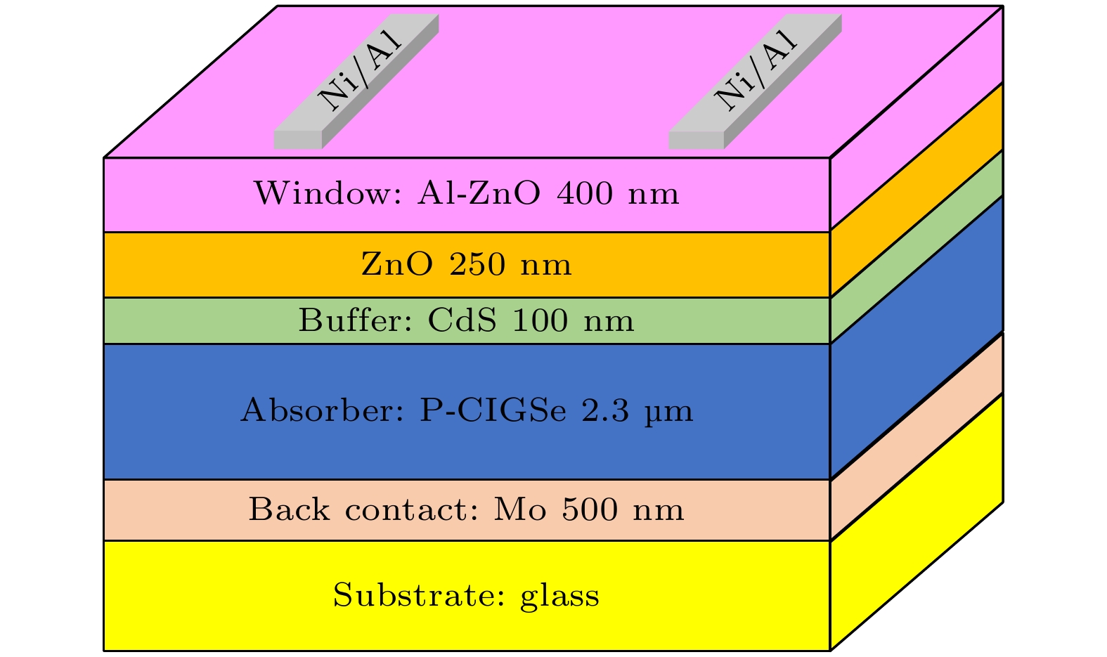
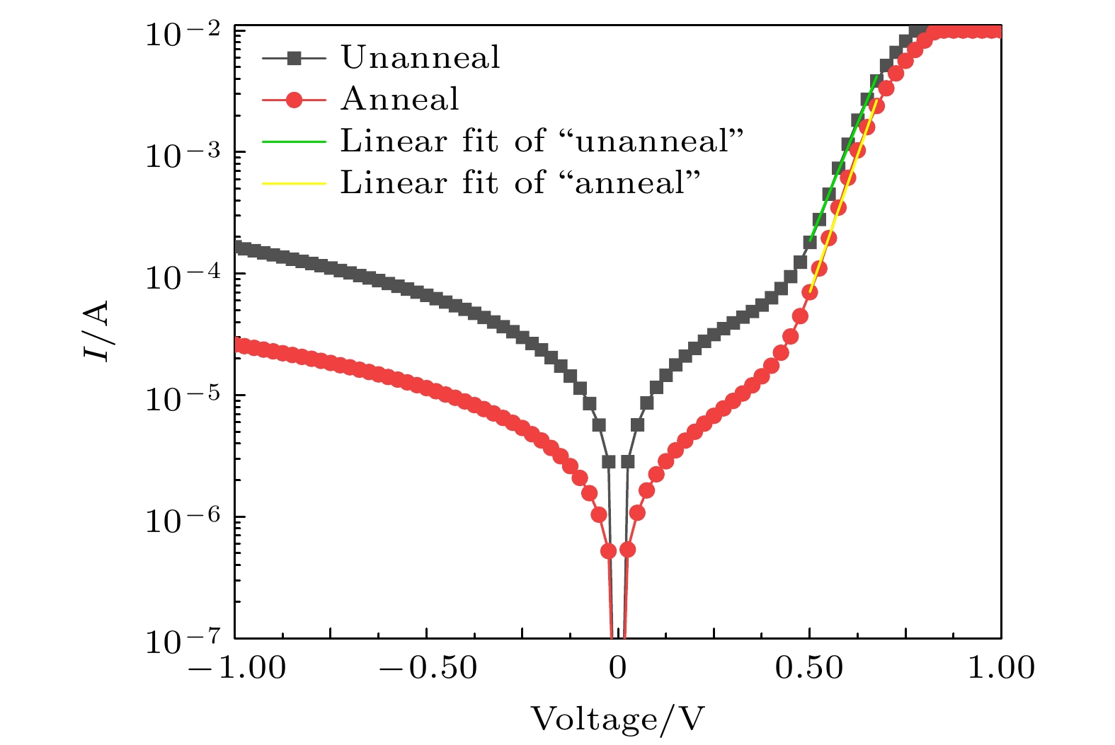
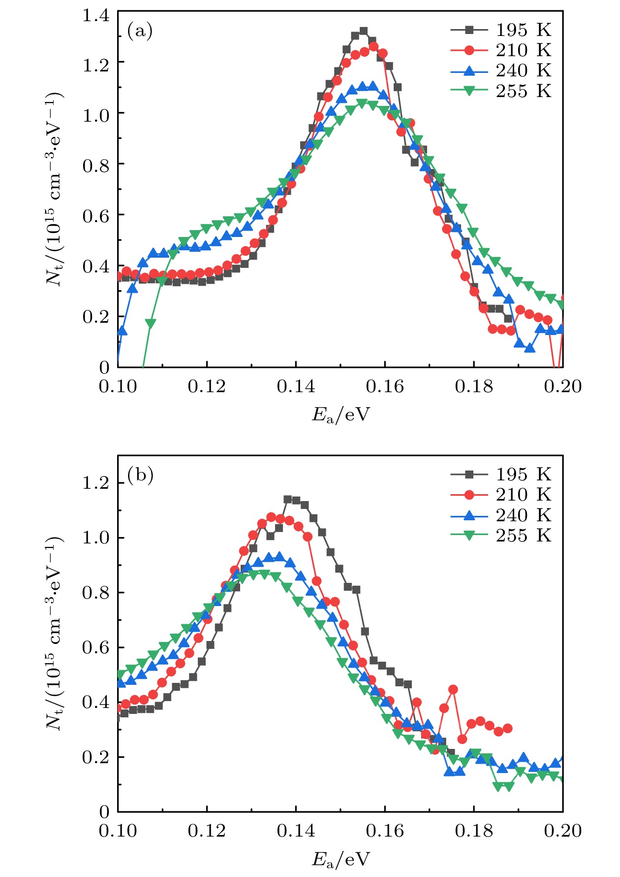
本文通过导纳谱技术表征铜铟镓硒(CIGSe)太阳电池吸收层中缺陷的能量分布, 研究了 CIGSe太阳电池退火后效率提高的机理. 研究发现退火后CIGSe电池的暗电流减小了大约1个数量级, 电池的理想因子也从退火前的2.16减小到退火后的1.85. 在反向偏压下, 退火前CIGSe太阳电池的电容高于退火后的. 通过对电池的C-V特性进行1/C 2-V线性拟合获得退火前CIGSe电池吸收层中的自由载流子浓度高于退火后, 此外还获得了CIGSe电池退火前后的内建电压分别为0.52 V和0.64 V. 通过导纳谱的测试发现退火后吸收层中缺陷的激活能降低, 但是缺陷浓度几乎不变. 缺陷激活能的降低意味着铜铟镓硒太阳能电池中缺陷的SRH (Shockley-read-hall)复合概率降低, 因此退火后太阳能电池的开路电压和并联电阻的增大提高了电池的性能.We use admittance spectroscopy to characterize the energy distribution of defects in CIGSe solar cells before and after annealing to investigate the mechanism of the annealing process improving the performances of solar cells. In this work, we anneal the prepared CIGSe solar cells in compressed air at 150 ℃ for 10 min. We measure dark I-V, C-V, admittance spectra, and illumination I-V tests on CIGSe solar cells before and after annealing to characterize the changes in the performances of solar cells before and after annealing, respectively. The test results of dark I-V characteristics show that the reverse dark current of CIGSe solar cell decreases by about an order of magnitude after annealing, and the ideal factor of the cell also decreases from 2.16 (before annealing) to 1.85 (after annealing). This means that the annealing process reduces the recombination of carriers in CIGSe solar cell. Under reverse bias, the capacitance of CIGSe solar cell is higher than that after annealing, and its C-V characteristics linearly fitted with 1/C 2 vs. V. The fitting results show that the slope of the curve increases after annealing, which means that the annealing process results in a decrease in the free carrier concentration in the absorption layer of CIGSe solar cell, specifically, the carrier concentration contributed by defects after annealing decreases. In addition, the built-in potential before and after annealing of CIGSe solar cell are also obtained through fitting, which are 0.52 V and 0.64 V in value, respectively. The admittance spectrum test results of CIGSe solar cell before and after annealing show that the defect activation energy in the absorption layer significantly decreases after annealing, but the defect concentration remains almost unchanged. The decrease in defect activation energy means that the Shockley Read Hall (SRH) recombination probability of defects in copper indium gallium selenium solar cell decreases. In addition, the test results of the optical I-V characteristics of the battery indicate that the open circuit voltage and parallel resistance of the solar cell significantly increase after annealing, which is consistent with the test results of the dark I-V characteristics, C-V characteristics, and admittance spectroscopy of the solar cell. Therefore, the annealing process of CIGSe solar cells leads to theweakening of the SRH recombination of carriers in the absorption layer of the cell, thereby improving the performance of the solar cell.
[1] Roulston D J, Arora N D, Chamberlain S G 1982 IEEE T. Electron Dev. 29 284
 Google Scholar
[2] Lang D V 1974 J. Appl. Phys. 45 3023
 Google Scholar
[3] Le Comber P G, Spear W E 1970 Phys. Rev. Lett. 25 509
 Google Scholar
[4] Bailey J, Zapalac G, Poplavskyy D 2016 IEEE 43rd Photovoltaic Specialists Conference (PVSC) Portland, OR, USA, June 5–10, 2016 p2135
[5] Hartmann F 2017 Springer Tracts in Modern Physics (Heidelberg: Springer Berlin) p275
[6] Bollmann J, Venter A 2018 Physica B 535 237
 Google Scholar
[7] Huang J S, Yuan Y B, Shao Y C 2017 Nat. Rev. Mater. 2 17042
[8] Gudovskikh A S, Kleider J P, Damon-Lacoste J, Roca I, Cabarrocas P, Veschetti Y, Muller J C, Ribeyron P J, Rolland E 2006 Thin Solid Films 511–512 385
 Google Scholar
[9] Walter T, Herberholz R, Müller C, Schock H W 1996 J. Appl. Phys. 80 4411
 Google Scholar
[10] Liguori R, Rubino A, 2021 Mater Today Proc 44 2033.
 Google Scholar
[11] Lee J, Cohen J D, Shafarman W N 2005 Thin Solid Films 480–481 336
 Google Scholar
[12] Dueñas S, Jaraiz M, Vicente J, Rubio E, Bailón L, Barbolla J 1987 J. Appl. Phys. 61 2541
 Google Scholar
[13] Burgelman M, Nollet P 2005 Solid State Ion. 176 2171
 Google Scholar
[14] Baranov A I, Kudryashov D A, Uvarov A V, et al. 2021 Tech. Phys. Lett. 47 785
 Google Scholar
[15] Karataş Ş, Türüt A 2004 Vacuum 74 45
 Google Scholar
[16] Marin A T, Musselman K P, MacManus-Driscoll J L 2013 J. Appl. Phys. 113 144502
 Google Scholar
[17] Kobayashi T, Kao Z J L, Nakada T 2015 Sol. Energy Mater Sol. Cells 143 159.
 Google Scholar
[18] Werner F, Siebentritt S 2018 Phys. Rev. Appl. 9 054047
 Google Scholar
[19] Heise S J, Hirwa H, Stölzel M, Dalibor T, Ohland J 2022 Thin Solid Films 759 1
[20] Paul S, Lopez R, Repins I L, Li J V 2018 J. Vac. Sci. Technol. B 36 022904
 Google Scholar
[21] Schroder D K 2015 Semiconductor Material and Device Characterization (John Wiley & Sons
[22] Sah C T 1991 Fundamentals of Solid-State Electronics (Singapore: World Scientific Publishing Company
-
-
[1] Roulston D J, Arora N D, Chamberlain S G 1982 IEEE T. Electron Dev. 29 284
 Google Scholar
[2] Lang D V 1974 J. Appl. Phys. 45 3023
 Google Scholar
[3] Le Comber P G, Spear W E 1970 Phys. Rev. Lett. 25 509
 Google Scholar
[4] Bailey J, Zapalac G, Poplavskyy D 2016 IEEE 43rd Photovoltaic Specialists Conference (PVSC) Portland, OR, USA, June 5–10, 2016 p2135
[5] Hartmann F 2017 Springer Tracts in Modern Physics (Heidelberg: Springer Berlin) p275
[6] Bollmann J, Venter A 2018 Physica B 535 237
 Google Scholar
[7] Huang J S, Yuan Y B, Shao Y C 2017 Nat. Rev. Mater. 2 17042
[8] Gudovskikh A S, Kleider J P, Damon-Lacoste J, Roca I, Cabarrocas P, Veschetti Y, Muller J C, Ribeyron P J, Rolland E 2006 Thin Solid Films 511–512 385
 Google Scholar
[9] Walter T, Herberholz R, Müller C, Schock H W 1996 J. Appl. Phys. 80 4411
 Google Scholar
[10] Liguori R, Rubino A, 2021 Mater Today Proc 44 2033.
 Google Scholar
[11] Lee J, Cohen J D, Shafarman W N 2005 Thin Solid Films 480–481 336
 Google Scholar
[12] Dueñas S, Jaraiz M, Vicente J, Rubio E, Bailón L, Barbolla J 1987 J. Appl. Phys. 61 2541
 Google Scholar
[13] Burgelman M, Nollet P 2005 Solid State Ion. 176 2171
 Google Scholar
[14] Baranov A I, Kudryashov D A, Uvarov A V, et al. 2021 Tech. Phys. Lett. 47 785
 Google Scholar
[15] Karataş Ş, Türüt A 2004 Vacuum 74 45
 Google Scholar
[16] Marin A T, Musselman K P, MacManus-Driscoll J L 2013 J. Appl. Phys. 113 144502
 Google Scholar
[17] Kobayashi T, Kao Z J L, Nakada T 2015 Sol. Energy Mater Sol. Cells 143 159.
 Google Scholar
[18] Werner F, Siebentritt S 2018 Phys. Rev. Appl. 9 054047
 Google Scholar
[19] Heise S J, Hirwa H, Stölzel M, Dalibor T, Ohland J 2022 Thin Solid Films 759 1
[20] Paul S, Lopez R, Repins I L, Li J V 2018 J. Vac. Sci. Technol. B 36 022904
 Google Scholar
[21] Schroder D K 2015 Semiconductor Material and Device Characterization (John Wiley & Sons
[22] Sah C T 1991 Fundamentals of Solid-State Electronics (Singapore: World Scientific Publishing Company
计量
- 文章访问数: 3822
- PDF下载量: 78
- 被引次数: 0


 下载:
下载:


