-
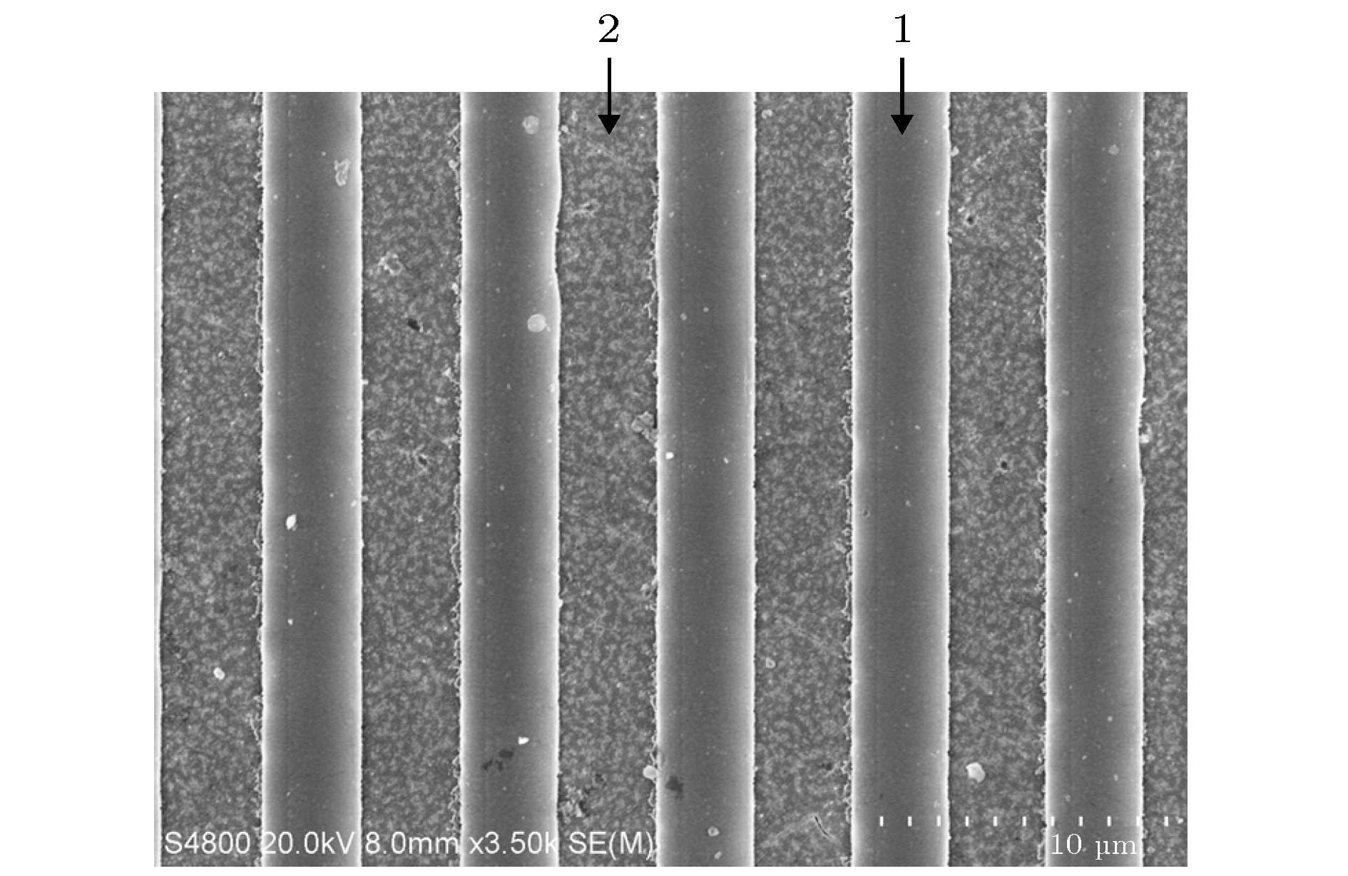
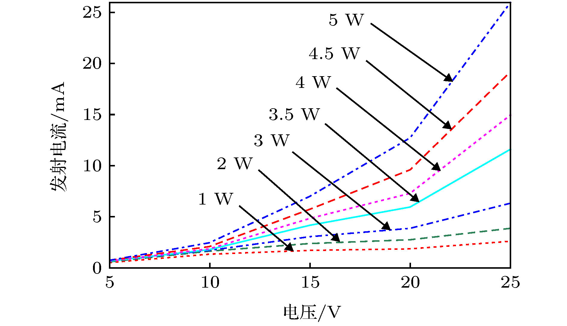
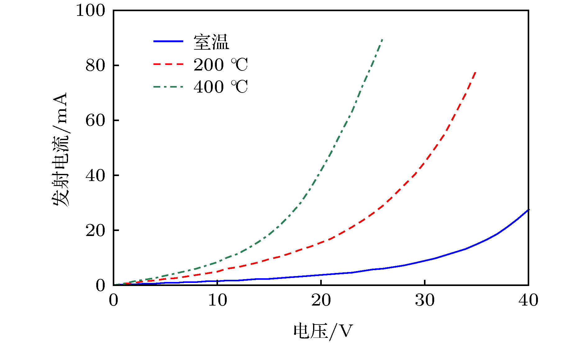
光电阴极的发射电流密度和寿命限制了其在功率器件和大科学装置中的应用. 本文结合光电阴极和场发射阴极电子发射理论, 设计了大电流密度的真空沟道结构光电阴极组件, 并使用覆膜和刻蚀技术制备了以GaAs衬底为阴极材料的光电阴极组件. 光电阴极组件电子发射特性测试结果显示, 常温状态下随入射光功率增加, 阴极发射电流增加幅度逐步增大. 光功率为5 W时, 发射电流达到26.12 mA, 电流密度达到5.33 A/cm2. 随光电阴极组件工作温度增加, 阴极材料内的载流子浓度也会相应地增加, 提高了负极对阴极材料内发射电子的补充效率, 增强了阴极组件的电子发射能力. 当光电阴极组件为400 ℃时, 其发射电流可达到89.69 mA. 由于阴极表面不存在激活原子, 在光电阴极组件连续144 h的寿命试验中, 阴极的发射电流为4.5 ± 0.3 mA, 阴极发射性能并未出现明显衰减. 真空沟道是光电阴极组件电子发射的主要区域, 通过改善真空沟道结构参数可以直接调整阴极组件发射电子束的形状, 增强大电流密度光电阴极在真空电子器件和设备中的适用性.The photocathode was an ideal electronic source with fast response, centralized distribution of electronic capabilities, and many other advantages. But for its low emission current density and short lifetime at ion bombardment environment, it will not be used in power devices and large scientific devices. Although the emission current of the photocathode can be increased with the aid of electric filed, it was not reach the milliamperelevel. In the field emission cathode, the strong electric field can effectively reduce the surface barrier of the emitter, so that the cathode produces electron emission. Based on the photoelectric conversion mechanism of photocathode and the electron emission theory of field emission cathode, a vacuum channel structure photocathode module is designed. The cathode modules with GaAs substrate were fabricated by the peritoneal and etching process. The parameters of vacuum channel were 3 μm × 700 μm, and its array structure was 1 × 100. The deep of the vacuum channels were 400 nm. It can be seen from the test result, the emission current of the photocathode was 26.12 mA with the laser beam power 5 W, and its emission current density was 5.33 A/cm2. During cathode operation, the laser beam and emission will cause the temperature of the photocathode material to rise, and this could icreasing the conductivity of the GaAs, the efficiency of electron supplement from negative electrode to electron emission area of the GaAs will also be improving. Its emission current could reach 89.69 mA at 400 ℃. Because there is no active atom on the photocathode surface, its lifetime was longer than the traditional photocathode that astivated by Cs/O. The life test of the photocathode modules was carried out, its emission current was 4.5 mA ± 0.3 mA within the 144 h, and its performance was not attenuate significantly. The vacuum channel was the main area of the photocatode electron emission, and the shape of electron beam can be easily obtained by adjusting the structure of the vacuum channel parameters. This advantage can improve the applicability of high current density photocathode in vacuum electronic devices and equipment.
-
Keywords:
- photocathode /
- current density /
- vacuum channel /
- lifetime
[1] Han J W, Oh J S, Meyyappan M 2012 Appl. Phys. Lett. 100 213505
 Google Scholar
[2] Tonouchi M 2007 Nat. Photonics 1 97
 Google Scholar
[3] Feng J J, Ren D P, Li H Y, Tang Y, Xing J Y 2011 Terahertz Sci. Technol. 4 164
[4] Stepanov A G, Hebling J, Kuhl J 2003 Appl. Phys. Lett. 83 3000
 Google Scholar
[5] Liu J F, Zhou Q L, Zhang C L 2013 Appl. Phys. Lett. 103 241911
 Google Scholar
[6] Kim J, Kim J, Oh H, Meyyappan M, Han J W, Lee J S 2016 J. Vac. Sci. Technol. B 34 042201
 Google Scholar
[7] Miao J S, Zhang S M, Cai L, Scherr M, Wang C 2015 Nano 9 9236
[8] Kim M, Kim H K 2015 J. Appl. Phys. 118 104504
 Google Scholar
[9] Gilad D, Er ez, Le eo 2008 Appl. Phys. Lett. 92 262903
 Google Scholar
[10] Zhao J, Chang B K, XiongY J, Zhang JJ, Zhang Y J 2012 Opt. Commun. 285 589
 Google Scholar
[11] 张益军, 牛军, 赵静, 邹继军, 常本康 2011 60 067301
 Google Scholar
Zhang Y J, Niu J, Zhao J, Zou J J, Chang B K 2011 Acta Phys. Sin. 60 067301
 Google Scholar
[12] Wang X H, Chang B K, Ren L, Gao P 2011 Appl. Phys. Lett. 98 082109
 Google Scholar
[13] Zhang Y J, Zou J J, Niu J, Zhao J, Chang B K 2011 J. Appl. Phys. 110 063113
 Google Scholar
[14] Hao G H, Yang M Z, Chang B K, Chen X L, Zhang J J, Fu X Q 2013 Appl. Opt. 52 5671
 Google Scholar
[15] 邹继军, 张益军, 杨智, 常本康 2011 60 017902
 Google Scholar
Zou J J, Zhang Y J, Yang Z, Chang B K 2011 Acta Phys. Sin. 60 017902
 Google Scholar
[16] Takuya H, Lothar M, Andreas L, Peter D, Peter H 2015 Appl. Phys. Lett. 106 051109
 Google Scholar
[17] Gys T 2015 Nucl. Instrum. Methods Phys. Res., Sect. A 787 254
 Google Scholar
[18] Chao Y C, Hu M C, Tsai W W, Zan H W, Meng H F, Tsai H K, Horng S F 2010 Appl. Phys. Lett. 97 223307
 Google Scholar
[19] 刘维浩, 张雅鑫, 胡旻, 周俊, 刘盛纲 2012 61 127901
 Google Scholar
Liu W H, Zhang Y X, Hu M, Zhou J, Liu S G 2012 Acta Phys. Sin. 61 127901
 Google Scholar
[20] Hsu S H, Kang W P, Wisitsora-at A, Davidson J L 2012 Diamond Relat. Mater. 22 142
 Google Scholar
[21] Hsu S H, Kang W P, Raina S, Howell M 2017 J. Vac. Sci. Technol. B 35 032201
 Google Scholar
-
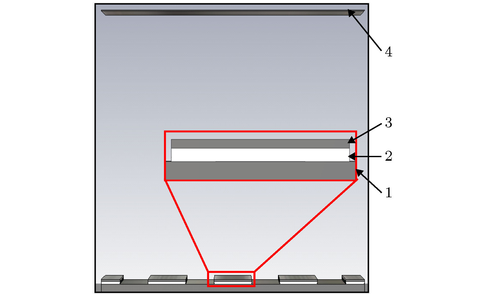
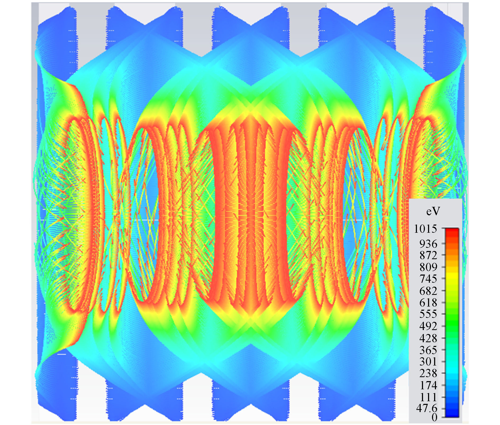
图 8 圆形真空沟道结构阴极组件电子发射特性仿真(a)结构模型; (b)横向截面中电子分布, 1为阴极材料, 2为绝缘层, 3为栅极
Fig. 8. Simulation of electronic emission characteristics of photocathode module with circular vacuum channel: (a) Structure model; (b) electronic distribution of lateral interface. Symbol 1, 2 and 3 are photocathode material, insulation, and grid electrode, respectively.
-
[1] Han J W, Oh J S, Meyyappan M 2012 Appl. Phys. Lett. 100 213505
 Google Scholar
[2] Tonouchi M 2007 Nat. Photonics 1 97
 Google Scholar
[3] Feng J J, Ren D P, Li H Y, Tang Y, Xing J Y 2011 Terahertz Sci. Technol. 4 164
[4] Stepanov A G, Hebling J, Kuhl J 2003 Appl. Phys. Lett. 83 3000
 Google Scholar
[5] Liu J F, Zhou Q L, Zhang C L 2013 Appl. Phys. Lett. 103 241911
 Google Scholar
[6] Kim J, Kim J, Oh H, Meyyappan M, Han J W, Lee J S 2016 J. Vac. Sci. Technol. B 34 042201
 Google Scholar
[7] Miao J S, Zhang S M, Cai L, Scherr M, Wang C 2015 Nano 9 9236
[8] Kim M, Kim H K 2015 J. Appl. Phys. 118 104504
 Google Scholar
[9] Gilad D, Er ez, Le eo 2008 Appl. Phys. Lett. 92 262903
 Google Scholar
[10] Zhao J, Chang B K, XiongY J, Zhang JJ, Zhang Y J 2012 Opt. Commun. 285 589
 Google Scholar
[11] 张益军, 牛军, 赵静, 邹继军, 常本康 2011 60 067301
 Google Scholar
Zhang Y J, Niu J, Zhao J, Zou J J, Chang B K 2011 Acta Phys. Sin. 60 067301
 Google Scholar
[12] Wang X H, Chang B K, Ren L, Gao P 2011 Appl. Phys. Lett. 98 082109
 Google Scholar
[13] Zhang Y J, Zou J J, Niu J, Zhao J, Chang B K 2011 J. Appl. Phys. 110 063113
 Google Scholar
[14] Hao G H, Yang M Z, Chang B K, Chen X L, Zhang J J, Fu X Q 2013 Appl. Opt. 52 5671
 Google Scholar
[15] 邹继军, 张益军, 杨智, 常本康 2011 60 017902
 Google Scholar
Zou J J, Zhang Y J, Yang Z, Chang B K 2011 Acta Phys. Sin. 60 017902
 Google Scholar
[16] Takuya H, Lothar M, Andreas L, Peter D, Peter H 2015 Appl. Phys. Lett. 106 051109
 Google Scholar
[17] Gys T 2015 Nucl. Instrum. Methods Phys. Res., Sect. A 787 254
 Google Scholar
[18] Chao Y C, Hu M C, Tsai W W, Zan H W, Meng H F, Tsai H K, Horng S F 2010 Appl. Phys. Lett. 97 223307
 Google Scholar
[19] 刘维浩, 张雅鑫, 胡旻, 周俊, 刘盛纲 2012 61 127901
 Google Scholar
Liu W H, Zhang Y X, Hu M, Zhou J, Liu S G 2012 Acta Phys. Sin. 61 127901
 Google Scholar
[20] Hsu S H, Kang W P, Wisitsora-at A, Davidson J L 2012 Diamond Relat. Mater. 22 142
 Google Scholar
[21] Hsu S H, Kang W P, Raina S, Howell M 2017 J. Vac. Sci. Technol. B 35 032201
 Google Scholar
计量
- 文章访问数: 9622
- PDF下载量: 171
- 被引次数: 0


 下载:
下载:
