-
U型槽的干法刻蚀工艺是GaN垂直沟槽型金属-氧化物-半导体场效应晶体管(MOSFET)器件关键的工艺步骤, 干法刻蚀后GaN的侧壁状况直接影响GaN MOS结构中的界面态特性和器件的沟道电子输运. 本文通过改变感应耦合等离子体干法刻蚀工艺中的射频功率和刻蚀掩模, 研究了GaN垂直沟槽型MOSFET电学特性的工艺依赖性. 研究结果表明, 适当降低射频功率, 在保证侧壁陡直的前提下可以改善沟道电子迁移率, 从35.7 cm2/(V·s)提高到48.1 cm2/(V·s), 并提高器件的工作电流. 沟道处的界面态密度可以通过亚阈值摆幅提取, 射频功率在50 W时界面态密度降低到1.90 × 1012 cm–2·eV–1, 比135 W条件下降低了一半. 采用SiO2硬刻蚀掩模代替光刻胶掩模可以提高沟槽底部的刻蚀均匀性. 较薄的SiO2掩模具有更小的侧壁面积, 高能离子的反射作用更弱, 过刻蚀现象明显改善, 制备出的GaN垂直沟槽型MOSFET沟道场效应迁移率更高, 界面态密度更低.
-
关键词:
- GaN垂直沟槽型金属-氧化物-半导体场效应晶体管 /
- U型槽 /
- 射频功率 /
- 刻蚀掩模
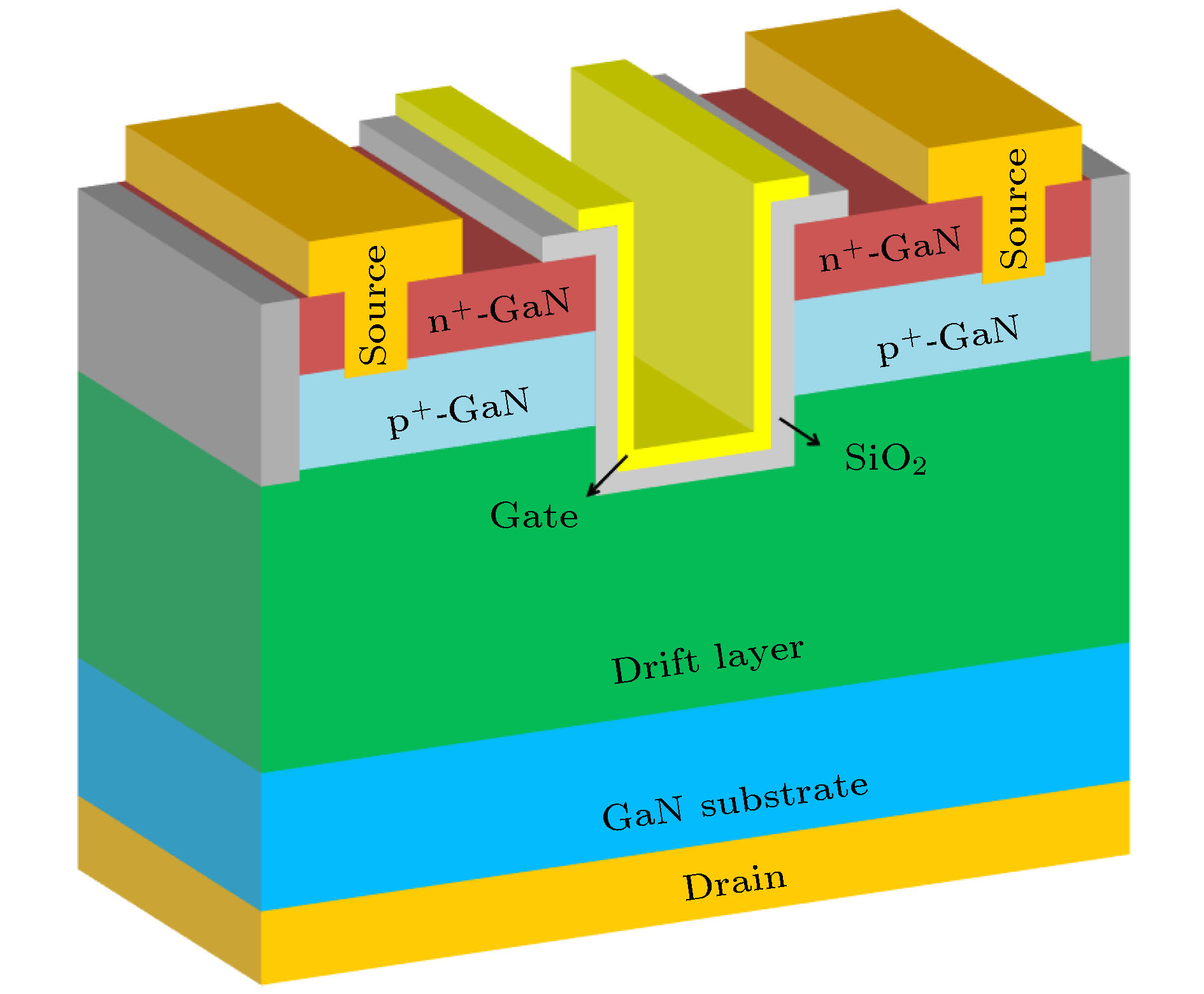
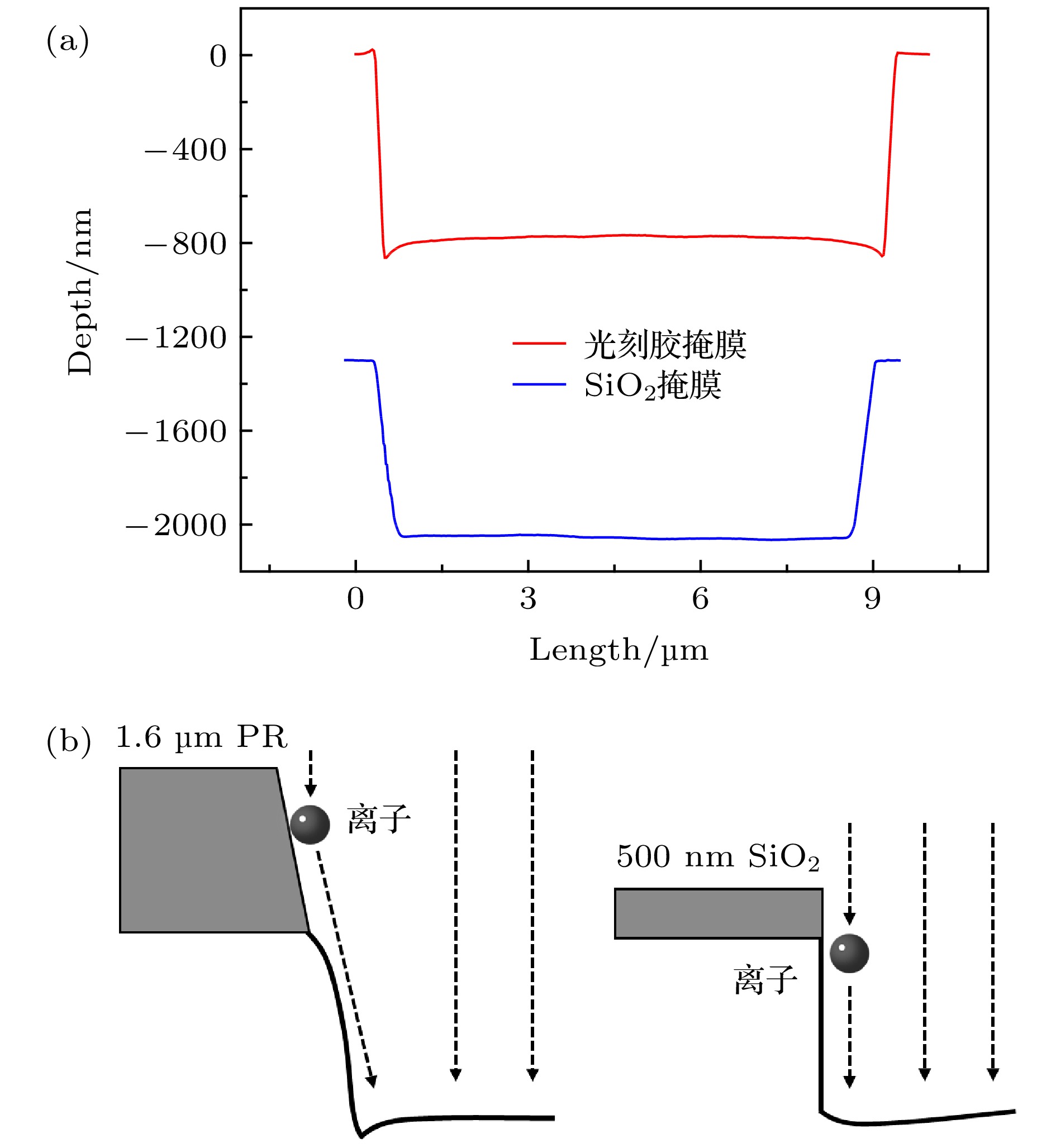
As reported by several market analysts, GaN-based power devices show great potential applications in the low and medium voltage range ( < 900 V). For high voltage ( > 1200 V), including ship transportation and power grid, the future applications of GaN highly depend on the development of vertical devices based on GaN substrates. Several vertical devices have been reported, such as current aperture vertical electron transistors (CAVETs), U-shape trench metal-oxide-semiconductor field-effect transistors (UMOSFETs), and fin power transistors. And the UMOSFETs show potential advantages due to greater simplicity in material epitaxy and fabrication process. In the fabrication of UMOSFETs, the U-shape trench dry etching is the most critical process. The GaN sidewalls after dry etching directly affect the interface state characteristics in the MOS structure and the channel electron transport. In this work, etching optimization including etching radio-frequency (RF) power and etching mask is investigated and process-dependent electrical characteristics of GaN UMOSFETs are also studied. The appropriate decrease of RF power ensuring the steep sidewalls can effectively improve the channel electron mobility from 35.7 cm2/(V·s) to 48.1 cm2/(V·s) and consequently increase the ON-state current and reduce the ON-state resistance. Larger etching damage to the p-GaN sidewall caused by higher RF power leads the scattering effects to increase and the mobility of the channel carriers to decrease. The interface state density at the channel can be extracted by the subthreshold swing. The interface state density decreases to 1.90 × 1012 cm–2·eV–1 when the RF power is regulated to 50 W, which is only half of the interface state density when RF power is 135 W. Similar breakdown voltages (350-380 V) are measured for these devices with varying RF power, which are governed by gate early breakdown. Positive valence band offset is formed in the SiO2/GaN MOS structure and the early breakdown occurs due to the holes accumulating at the SiO2/GaN interface. The etching uniformity at the bottom of U-shape trench can be improved by using the SiO2 hard masks instead of photoresist masks. Sub-trenches at both ends of the trench bottom are observed in the device with photoresist masks, leading the carrier scattering to increase and ON-state current to decrease. Besides, the interface state density decreases from 3.42 × 1012 cm–2·eV–1 to 2.46 × 1012 cm–2·eV–1 with a SiO2 hard mask layer used. Compared with 1.6 μm photoresist mask, the thinner SiO2 mask with a thickness of 500 nm has a small sidewall area, which weakens the high-energy ion reflection in the inductively coupled plasma system. Consequently, the over-etching at the bottom ends of the trench is improved significantly and therefore the fabricated GaN UMOSFET has higher channel mobility and a lower interface state density.-
Keywords:
- GaN vertical trench metal-oxide-semiconductor field-effect transistor /
- U-shape trench /
- radio-frequency power /
- etching mask
[1] Uemoto Y, Hikita M, Ueno H, Matsuo H, Ishida H, Yanagihara M, Ueda T, Tanaka T, Ueda D 2007 IEEE Trans. Electron Dev. 54 3393
 Google Scholar
[2] Anderson T J, Wheeler V D, Shahin D I, Tadjer M J, Koehler A D, Hobart K D, Christou A, Kub F J, Eddy C R 2016 Appl. Phys. Express 9 071003
 Google Scholar
[3] Sun S, Fu K, Yu G, Zhang Z, Song L, Deng X, Qi Z, Li S, Sun Q, Cai Y, Dai J, Chen C, Zhang B 2016 Appl. Phys. Lett. 108 013507
 Google Scholar
[4] Wang H, Wang J, Liu J, Li M, He Y, Wang M, Yu M, Wu W, Zhou Y, Dai G 2017 Appl. Phys. Express 10 106502
 Google Scholar
[5] Gao J, Jin Y, Xie B, Wen C P, Hao Y, Shen B, Wang M 2018 IEEE Electron Dev. Lett. 39 859
 Google Scholar
[6] Ambacher O, Smart J, Shealy J R, Weimann N G, Chu K, Murphy M, Schaff W J, Eastman L F, Dimitrov R, Wittmer L, Stutzmann M, Rieger W, Hilsenbeck J 1999 J. Appl. Phys. 85 3222
 Google Scholar
[7] Kambayashi H, Satoh Y, Kokawa T, Ikeda N, Nomura T, Kato S 2011 Solid-State Electron. 56 163
 Google Scholar
[8] 崔兴涛, 陈万军, 施宜军, 信亚杰, 李茂林, 王方洲, 周琦, 李肇基, 张波 2019 半导体技术 44 286
 Google Scholar
Cui X T, Chen W J, Shi Y J, Xin Y J, Li M L, Wang F Z, Zhou Q, Li Z J, Zhang B 2019 Semiconductor Technology 44 286
 Google Scholar
[9] 唐文昕, 郝荣晖, 陈扶, 于国浩, 张宝顺 2018 67 198501
 Google Scholar
Tang W X, Hao R H, Chen F, Yu G H, Zhang B S 2018 Acta Phys. Sin. 67 198501
 Google Scholar
[10] Lin R M, Chu F C, Das A, Liao S Y, Chou S T, Chang L B 2013 Thin Solid Films 544 526
 Google Scholar
[11] Russo S, Di Carlo A 2007 IEEE Trans. Electron Dev. 54 1071
 Google Scholar
[12] Horio K, Takayanagi H, Nakano H 2006 Phys. Status Solidi 3 2346
 Google Scholar
[13] Meneghesso G, Rampazzo F, Kordos P, Verzellesi G, Zanoni E 2007 IEEE Trans. Electron Dev. 53 2932
 Google Scholar
[14] Oka T, Ina T, Ueno Y, Nishii J 2015 Appl. Phys. Express 8 054101
 Google Scholar
[15] Chowdhury S, Swenson B L, Wong M H, Mishra U K 2013 Semicond. Sci. Technol. 28 074014
 Google Scholar
[16] Nie H, Diduck Q, Alvarez B, Edwards A P, Kayes B M, Zhang M, Ye G, Prunty T, Bour D, Kizilyalli I C 2014 IEEE Electron Dev. Lett. 35 939
 Google Scholar
[17] Ji D, Chowdhury S 2015 IEEE Trans. Electron Dev. 62 2571
 Google Scholar
[18] Otake H, Chikamatsu K, Yamaguchi A, Fujishima T, Ohta H 2008 Appl. Phys. Express 1 011105
 Google Scholar
[19] Oka T, Ueno Y, Ina T, Hasegawa K 2014 Appl. Phys. Express 7 021002
 Google Scholar
[20] Sun M, Zhang Y, Gao X, Palacios T 2017 IEEE Electron Dev. Lett. 38 509
 Google Scholar
[21] Zhang Y, Sun M, Perozek J, Liu Z, Zubair A, Piedra D, Chowdhury N, Gao X, Shepard K, Palacios T 2018 IEEE Electron Dev. Lett. 40 75
 Google Scholar
[22] Gupta C, Chan S H, Lund C, Agarwal A, Koksaldi O S, Liu J, Enatsu Y, Keller S, Mishra U K 2016 Appl. Phys. Express 9 121001
 Google Scholar
[23] Fujishima T, Otake H, Ohta H 2008 Appl. Phys. Lett. 92 243505
 Google Scholar
[24] Wang Q, Jiang Y, Zhang J, Kawaharada K, Li L, Wang D, Ao J P 2015 Semicond. Sci. Technol. 30 065004
 Google Scholar
[25] 施罗德 D K 著 (刘爱民等 译) 1998 半导体材料与器件表征技术 (大连: 大连理工大学出版社) 第284−286页
Schroder D K (translated by Liu A M) 1998 Semiconductor Material and Device Characterization (Dalian: Dalian University of Technology Press) pp284−286 (in Chinese)
[26] Gupta C, Chan S, Pasayat S, Keller S, Mishra U 2019 J. Appl. Phys. 125 124101
 Google Scholar
[27] Narita T, Kikuta D, Takahashi N, Kataoka K, Kimoto Y, Uesugi T, Kachi T, Sugimoto M 2011 Phys. Status Solidi A 208 1541
 Google Scholar
[28] Kodama M, Sugimoto M, Hayashi E, Soejima N, Ishiguro O, Kanechika M, Itoh K, Ueda H, Uesugi T, Kachi T 2008 Appl. Phys. Express 1 021104
 Google Scholar
[29] Flemish J R, Xie K 1994 Appl. Phys. Lett. 64 2315
 Google Scholar
-
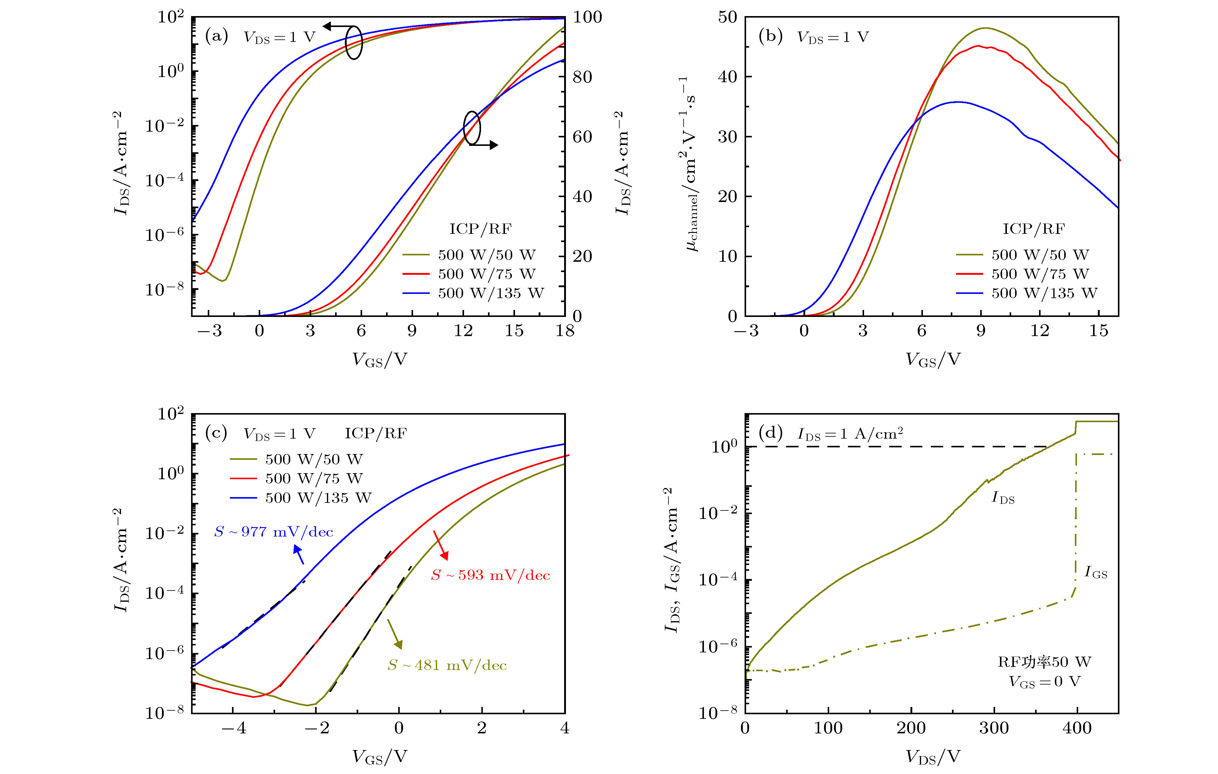
图 2 干法刻蚀RF功率为50, 75和135 W制备出GaN UMOSFET器件的电学特性曲线(IGS和IDS分别指栅电流和漏电流) (a)转移特性曲线; (b)沟道场效应迁移率随栅电压VGS的变化曲线; (c)亚阈值特性; (d) RF功率50 W的器件三端击穿特性
Fig. 2. Electrical characteristics of GaN UMOSFETs fabricated with RF power of 50, 75 and 135 W (IGS and IDS are gate and drain currents): (a) Transfer characteristics; (b) field-effect channel mobility as a function of gate voltage; (c) subthreshold characteristics; (d) breakdown characteristics.
图 3 采用光刻胶和SiO2作为刻蚀掩模制备出的GaN UMOSFET器件的电学特性曲线 (a)转移特性曲线; (b)沟道场效应迁移率随栅电压的变化曲线; (c)输出特性曲线; (d)亚阈值特性
Fig. 3. Electrical characteristics of GaN UMOSFETs with SiO2 and photoresist as etching masks: (a) Transfer characteristics; (b) field-effect channel mobility vs. gate voltage; (c) output
$ I\text-V $ characteristics; (d) subthreshold characteristics.表 1 干法刻蚀条件参数(1 Torr = 1.33322 × 10² Pa)
Table 1. Experiment parameters of the dry etching process.
条件 刻蚀气体及流量 RF功率/W ICP功率/W 腔室压强/mTorr 刻蚀掩模 A 24 sccm Cl2, 16 sccm BCl3, 5 sccm Ar 135 500 8 光刻胶(PR) B 75 C 50 D 50 SiO2 -
[1] Uemoto Y, Hikita M, Ueno H, Matsuo H, Ishida H, Yanagihara M, Ueda T, Tanaka T, Ueda D 2007 IEEE Trans. Electron Dev. 54 3393
 Google Scholar
[2] Anderson T J, Wheeler V D, Shahin D I, Tadjer M J, Koehler A D, Hobart K D, Christou A, Kub F J, Eddy C R 2016 Appl. Phys. Express 9 071003
 Google Scholar
[3] Sun S, Fu K, Yu G, Zhang Z, Song L, Deng X, Qi Z, Li S, Sun Q, Cai Y, Dai J, Chen C, Zhang B 2016 Appl. Phys. Lett. 108 013507
 Google Scholar
[4] Wang H, Wang J, Liu J, Li M, He Y, Wang M, Yu M, Wu W, Zhou Y, Dai G 2017 Appl. Phys. Express 10 106502
 Google Scholar
[5] Gao J, Jin Y, Xie B, Wen C P, Hao Y, Shen B, Wang M 2018 IEEE Electron Dev. Lett. 39 859
 Google Scholar
[6] Ambacher O, Smart J, Shealy J R, Weimann N G, Chu K, Murphy M, Schaff W J, Eastman L F, Dimitrov R, Wittmer L, Stutzmann M, Rieger W, Hilsenbeck J 1999 J. Appl. Phys. 85 3222
 Google Scholar
[7] Kambayashi H, Satoh Y, Kokawa T, Ikeda N, Nomura T, Kato S 2011 Solid-State Electron. 56 163
 Google Scholar
[8] 崔兴涛, 陈万军, 施宜军, 信亚杰, 李茂林, 王方洲, 周琦, 李肇基, 张波 2019 半导体技术 44 286
 Google Scholar
Cui X T, Chen W J, Shi Y J, Xin Y J, Li M L, Wang F Z, Zhou Q, Li Z J, Zhang B 2019 Semiconductor Technology 44 286
 Google Scholar
[9] 唐文昕, 郝荣晖, 陈扶, 于国浩, 张宝顺 2018 67 198501
 Google Scholar
Tang W X, Hao R H, Chen F, Yu G H, Zhang B S 2018 Acta Phys. Sin. 67 198501
 Google Scholar
[10] Lin R M, Chu F C, Das A, Liao S Y, Chou S T, Chang L B 2013 Thin Solid Films 544 526
 Google Scholar
[11] Russo S, Di Carlo A 2007 IEEE Trans. Electron Dev. 54 1071
 Google Scholar
[12] Horio K, Takayanagi H, Nakano H 2006 Phys. Status Solidi 3 2346
 Google Scholar
[13] Meneghesso G, Rampazzo F, Kordos P, Verzellesi G, Zanoni E 2007 IEEE Trans. Electron Dev. 53 2932
 Google Scholar
[14] Oka T, Ina T, Ueno Y, Nishii J 2015 Appl. Phys. Express 8 054101
 Google Scholar
[15] Chowdhury S, Swenson B L, Wong M H, Mishra U K 2013 Semicond. Sci. Technol. 28 074014
 Google Scholar
[16] Nie H, Diduck Q, Alvarez B, Edwards A P, Kayes B M, Zhang M, Ye G, Prunty T, Bour D, Kizilyalli I C 2014 IEEE Electron Dev. Lett. 35 939
 Google Scholar
[17] Ji D, Chowdhury S 2015 IEEE Trans. Electron Dev. 62 2571
 Google Scholar
[18] Otake H, Chikamatsu K, Yamaguchi A, Fujishima T, Ohta H 2008 Appl. Phys. Express 1 011105
 Google Scholar
[19] Oka T, Ueno Y, Ina T, Hasegawa K 2014 Appl. Phys. Express 7 021002
 Google Scholar
[20] Sun M, Zhang Y, Gao X, Palacios T 2017 IEEE Electron Dev. Lett. 38 509
 Google Scholar
[21] Zhang Y, Sun M, Perozek J, Liu Z, Zubair A, Piedra D, Chowdhury N, Gao X, Shepard K, Palacios T 2018 IEEE Electron Dev. Lett. 40 75
 Google Scholar
[22] Gupta C, Chan S H, Lund C, Agarwal A, Koksaldi O S, Liu J, Enatsu Y, Keller S, Mishra U K 2016 Appl. Phys. Express 9 121001
 Google Scholar
[23] Fujishima T, Otake H, Ohta H 2008 Appl. Phys. Lett. 92 243505
 Google Scholar
[24] Wang Q, Jiang Y, Zhang J, Kawaharada K, Li L, Wang D, Ao J P 2015 Semicond. Sci. Technol. 30 065004
 Google Scholar
[25] 施罗德 D K 著 (刘爱民等 译) 1998 半导体材料与器件表征技术 (大连: 大连理工大学出版社) 第284−286页
Schroder D K (translated by Liu A M) 1998 Semiconductor Material and Device Characterization (Dalian: Dalian University of Technology Press) pp284−286 (in Chinese)
[26] Gupta C, Chan S, Pasayat S, Keller S, Mishra U 2019 J. Appl. Phys. 125 124101
 Google Scholar
[27] Narita T, Kikuta D, Takahashi N, Kataoka K, Kimoto Y, Uesugi T, Kachi T, Sugimoto M 2011 Phys. Status Solidi A 208 1541
 Google Scholar
[28] Kodama M, Sugimoto M, Hayashi E, Soejima N, Ishiguro O, Kanechika M, Itoh K, Ueda H, Uesugi T, Kachi T 2008 Appl. Phys. Express 1 021104
 Google Scholar
[29] Flemish J R, Xie K 1994 Appl. Phys. Lett. 64 2315
 Google Scholar
计量
- 文章访问数: 17737
- PDF下载量: 308
- 被引次数: 0


 下载:
下载:


