-
以金纳米棒垂直阵列(gold-nanorods vertical array, GVA)为衬底, SiO2为隔离层, 构建GVA@SiO2@NaYF4:Yb3+/Er3+纳米复合结构. 在近红外980 nm激发下, 通过改变中间隔离层SiO2的厚度, 研究GVA对NaYF4:Yb3+/Er3+纳米晶体上转换发光的调控规律. 实验结果表明, 当SiO2层的厚度增大至8 nm时, Er3+离子整体的上转换发射强度增大近8.8倍, 且红光强度增强尤为明显, 约为16.2倍. 为了进一步证实GVA对Er3+离子红光发射的增强效果, 以红光发射为主的NaYF4:40%Yb3+/2%Er3+纳米晶体为对象展开研究, 发现Er3+离子红绿比由1.84增加到2.08, 证实该复合结构更有利于提高红光的发射强度. 通过对其光谱特性、发光动力学过程的研究并结合其理论模拟, 证实了上转换发光的增强是由激发与发射增强共同作用, 而激发增强占据主导地位. 采用该套复合体结构实现上转换荧光发射的增强, 不仅有效地利用了贵金属的等离激元共振特性, 而且对深入理解等离激元增强上转换发光的物理机理提供理论依据.
-
关键词:
- 上转换发光 /
- 金纳米棒垂直阵列 /
- NaYF4:Yb3+/Er3+纳米晶体 /
- 等离激元
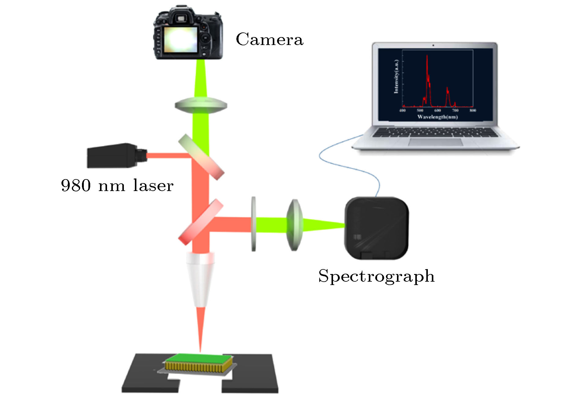
The plasmon resonance effect is one of the effective ways to enhance the upconversion (UC) luminescence, which is realized by enhancing the electromagnetic field from incident light interacting with free electrons of AuNRs surface. In this work, a series of GVA@SiO2@NaYF4:Yb3+/Er3+ composite structures with different thickness values of SiO2 isolation layer is successfully built from self-assembled gold nanorods, steamed SiO2, and spin-coating rare-earth nanocrystals. The results of the SEM indicate that the size of gold-nanorods is approximately 22 nm in diameter and 65 nm in length. The X-ray diffraction and transmission electron microscope results demonstrate that the NaYF4:Yb3+/Er3+ nanocrystals possess hexagonal-phase structure with a size of about 20 nm. Under 980 nm near-infrared (NIR) excitation, the UC emission characteristics of GVA@SiO2@NaYF4:Yb3+/Er3+ composite structure are studied by using a confocal microscope spectroscopic test system, and regulated by changing the thickness of SiO2 isolation layer. The results indicate that the UC emission intensity of NaYF4:20%Yb3+/2%Er3+ nanocrystals is enhanced by about 8.8 times, and the enhancement factor of red UC emission intensity is about 16.2. In order to further prove the enhancement effect of the red UC emission, the GVA@SiO2@NaYF4:40%Yb3+/20%Er3+ composite structure with red UC emission is constructed in the same way. It can be found that the UC emission intensity of NaYF4:40%Yb3+/20%Er3+ nanocrystals is enhanced by 8.7 times and the red UC emission intensity is raised by about 9.7 times under the 980 nm NIR excitation. The corresponding excitation enhancement mechanism is simulated according to the power excitation dependence. And it is found that the rate of UC emission decreases and the R/G ratio also decreases with the excitation pump power increasing. The analysis of the above results shows that the excitation enhancement plays a leading role and is accompanied by emission enhancement. Meanwhile, the study of Er3+ ion dynamic process indicates that the Er3+ ion transition rate is accelerated due to the coupling from UC emission peaks and gold nanorod absorption peaks in GVA@SiO2@NaYF4:40%Yb3+/20%Er3+ composite structure. The enhancement mechanism of UC emission is also simulated, which further proves that the excitation enhancement is dominant. This kind of composite structure can not only help us to further understand the physics mechanism of the plasmon-enhanced UC luminescence but also promote the applications of rare-earth materials in medical imaging and fingerprint recognition.-
Keywords:
- upconversion emission /
- gold-nanorods vertical array /
- NaYF4:Yb3+/Er3+ nanocrystals /
- plasmon
[1] Runowski M, Stopikowska N, Szeremeta D, Goderski S, Skwierczyńska M, Lis S 2019 ACS. Appl. Mat. Inter. 11 13389
 Google Scholar
[2] Hassan A M, Wu X, Jarrett J W, et al. 2019 Biomed. Opt. Express 10 584
 Google Scholar
[3] Zhou B, Shi B Y, Jin D Y, Liu X G 2015 Nat. Nanotechnol. 10 924
 Google Scholar
[4] Wang M, Li M, Yu A, Wu J, Mao C 2015 ACS. Appl. Mat. Inter. 7 28110
 Google Scholar
[5] Gong G, Song Y, Tan H H, Xie S W, Zhang C F, Xu L J, Xu J X, Zheng J 2019 Compos. Part B-Eng. 179 107504
 Google Scholar
[6] Chen G Y, Damasco J, Qiu H L, et al. 2015 Nano. Lett. 15 7400
 Google Scholar
[7] 何恩节, 郑海荣, 高伟, 等 2013 62 237803
 Google Scholar
He E J, Zheng H R, Gao W, et al. 2013 Acta Phys. Sin. 62 237803
 Google Scholar
[8] Dong J, Zhang J, Han Q, Zhao X, Yan X W, Liu J H, Ge H B, Gao W 2019 J. Lumin. 207 361
 Google Scholar
[9] Dong J, Gao W, Han Q, Wang Y K, Qia J X, Yan X W, Sun M T 2018 Rev. Math. Phys. 4 100026
 Google Scholar
[10] 韩庆艳, 高伟, 祁建霞, 张成云, 赵星, 张正龙, 董军, 郑海荣 2018 中国科学: 物理学 力学 天文学 48 82
 Google Scholar
Han Q Y, Gao W, Qi J X, Zhang C Y, Zhao X, Zhang Z L, Dong J, Zheng H R 2018 Sci. Sin-Phys. Mech. Astron. 48 82
 Google Scholar
[11] Dong J, Zhang Z L, Zheng H R, Sun M T 2015 Nanophotonics-Berlin 4 472
 Google Scholar
[12] Park W, Lu D W, Ahn S 2015 Chem. Soc. Rev. 44 2940
 Google Scholar
[13] Feng W, Sun L D, Yan C H 2009 Chem. Commun. 29 4393
 Google Scholar
[14] Dong J, Zhao X, Cao E, et al. 2020 Mater. Today 9 100067
 Google Scholar
[15] Clarke C, Liu D, Wang F, e al. 2018 Nanoscale 10 6270
 Google Scholar
[16] Wang Q R, Zhang J, Sang X, Zhang D, Shi Q, Li S H, Wang W J 2018 J. Lumin. 204 284
 Google Scholar
[17] Zong H, Mu X J, Sun M T 2019 Appl. Mater. Today 15 43
 Google Scholar
[18] Das A, Mao C C, Cho S, Kim K, Park W 2018 Nat. Commun. 9 4828
 Google Scholar
[19] He E J, Yu J J, Wang C, Jiang Y, Zuo X Z, Xu B, Wen J, Qin Y F, Wang Z J 2020 Mater. Res. Bull. 121 110613
 Google Scholar
[20] Xu W, Chen X, Song H W 2017 Nano. Today 17 54
 Google Scholar
[21] Ji Y N, Xu W, Li D Y, Zhou D L, Chen X, Ding N, Li J, Wang N, Bai X, Song H W 2019 Nano. Energy 61 211
 Google Scholar
[22] Yin Z, Zhou D L, Xu W, Cui S B, Chen X, Wang H, Xu S H, Song H W 2016 ACS. Appl. Mat. Inter. 8 11667
 Google Scholar
[23] Kang F W, He J J, Sun T Y, Bao Z Y, Wang F, Lei D Y 2017 Adv. Funct. Mater. 27 1701842
 Google Scholar
[24] Gao W, Wang B Y, Han Q Y, Gao L, Wang Z J, Sun Z Y, Zhang B, Dong J 2020 J. Alloy. Compd. 818 152934
 Google Scholar
[25] Nikoobakht B, El-Sayed M A 2003 Chem. Mater. 15 1957
 Google Scholar
[26] Dong J, Zhao X, Gao W, Han Q Y, Qi J X, Wang Y K, Guo S D, Sun M T 2019 Nanoscale. Res. Lett. 14 118
 Google Scholar
[27] Man X K, D oi, M 2016 Phys Rev Lett, 116 066101
 Google Scholar
[28] Gao W, Kong X Q, Han Q Y, et al. 2018 J. Lumin. 196 187
 Google Scholar
[29] 高伟, 董军 2017 66 204206
 Google Scholar
Gao W, Dong J 2017 Acta Phys. Sin. 66 204206
 Google Scholar
[30] Liu X, Lei D Y 2015 Sci. Rep-Uk. 5 15235
 Google Scholar
[31] Rohani S, Quintanilla M, Tuccio S, et al. 2015 Adv. Opt. Mater. 3 1606
 Google Scholar
[32] Wang T, Siu C K, Yu H, et al. 2018 Inorg. Chem. 57 8200
 Google Scholar
[33] Saboktakin M, Ye X C, Oh S J, et al. 2012 ACS Nano 6 8758
 Google Scholar
[34] Feng A L, You M L, Tian L M, Singamaneni S, Lin M, Duan Z F, Lu T J, Xu F, Lin M 2015 Sci. Rep-Uk. 5 7779
 Google Scholar
[35] Green K, Wirth J, Lim S F 2016 Nanotechnology 27 135201
 Google Scholar
[36] 严学文, 王朝晋, 王博扬, 等 2019 68 174204
 Google Scholar
Yan X W, Wang Z J, Wang B Y, et al. 2019 Acta Phys. Sin. 68 174204
 Google Scholar
[37] Elrafei S A, Kandas I, Shehata N, Samir E, Okaz A, Rizk M 2018 J. Lumin. 204 581
 Google Scholar
[38] Schietinger S, Aichele T, Wang H Q, Nann T, Benson O 2009 Nano Lett. 10 134
 Google Scholar
[39] Saboktakin M, Ye X C, Chettiar U K, Engheta N, Murray C B, Kagan C R 2013 ACS Nano 7 7186
 Google Scholar
[40] Zhao X, Dong J, Cao E, Han Q Y, Gao W, Wang Y K, Qi J X, Sun M T 2019 Appl. Mater. Today 14 166
 Google Scholar
[41] Jung K 2019 B Korean Chem. Soc. 40 91
 Google Scholar
-
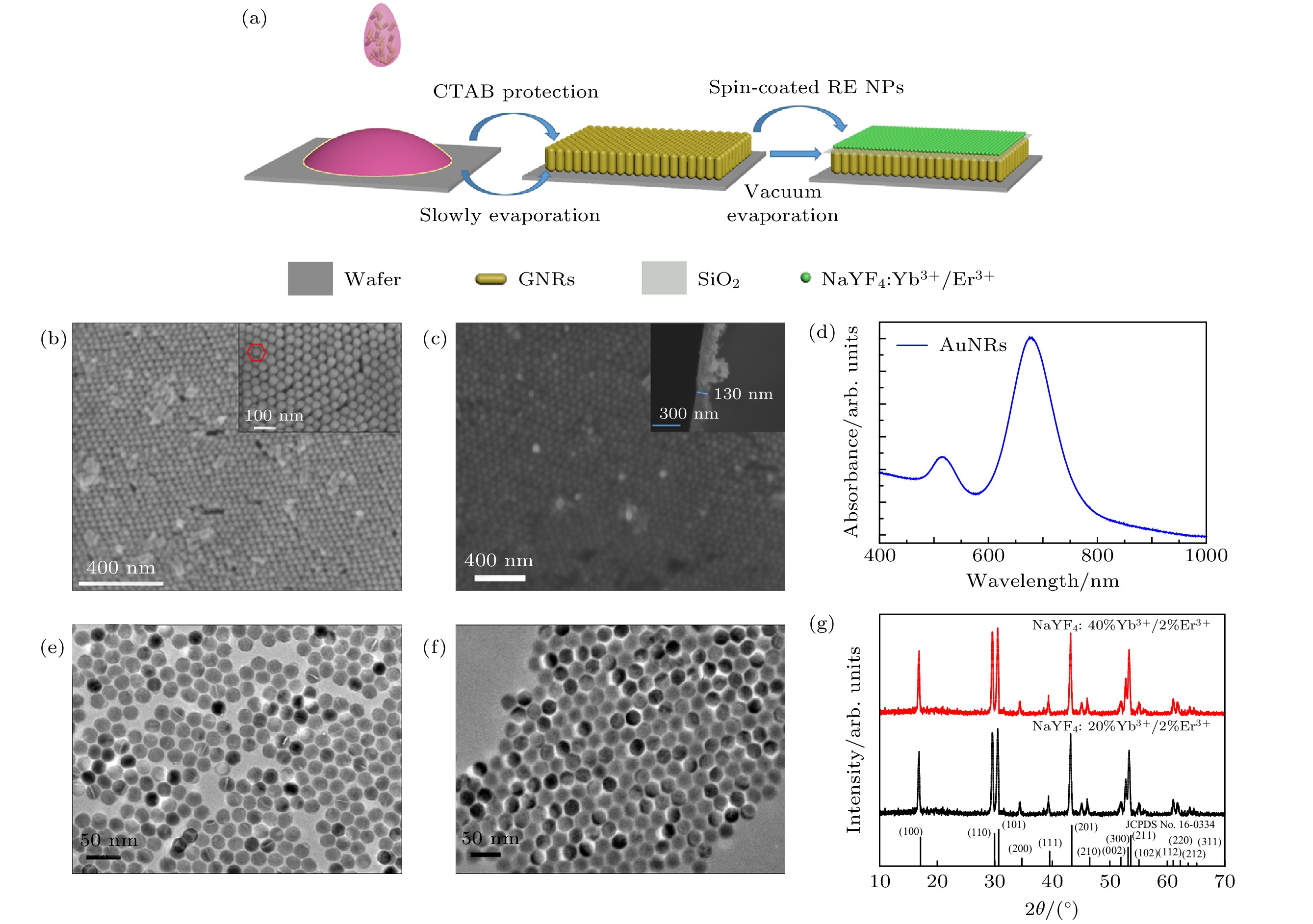
图 1 (a) GVA@SiO2@NaYF4:Yb3+/Er3+复合发光体系构建的示意图; (b) GVA大规模SEM图; (c) GVA@SiO2 (8 nm)的SEM图, 右上角的插图为旋涂NaYF4:Yb3+/Er3+纳米晶体后的SEM截面图; (d) GNRs的吸收谱, 插图为相应的SEM图; (e)和(f)分别为NaYF4:20%Yb3+/2%Er3+和NaYF4:40%Yb3+/2%Er3+纳米晶体的TEM图; (g)为NaYF4:20%Yb3+/2%Er3+和NaYF4:40%Yb3+/2%Er3+纳米晶体的的XRD图
Fig. 1. (a) Construction scheme of the preparation process of GVA@SiO2@NaYF4:Yb3+/Er3+; (b) the typical SEM images of the large-scale and corresponding small-scale GVA; (c) the SEM images of the GVA@SiO2 (8 nm), and the cross-sectional view of the spin-coated NaYF4:Yb3+/Er3+ nanocrystals; (d) the ultraviolet-visible absorption spectrum of GNRs; TEM images of (e) NaYF4:20%Yb3+/2%Er3+ and (f) NaYF4: 40%Yb3+/2%Er3+ nanocrystals; (g) XRD patterns of NaYF4:20%Yb3+/2%Er3+ and NaYF4: 40%Yb3+/2%Er3+ nanocrystals.
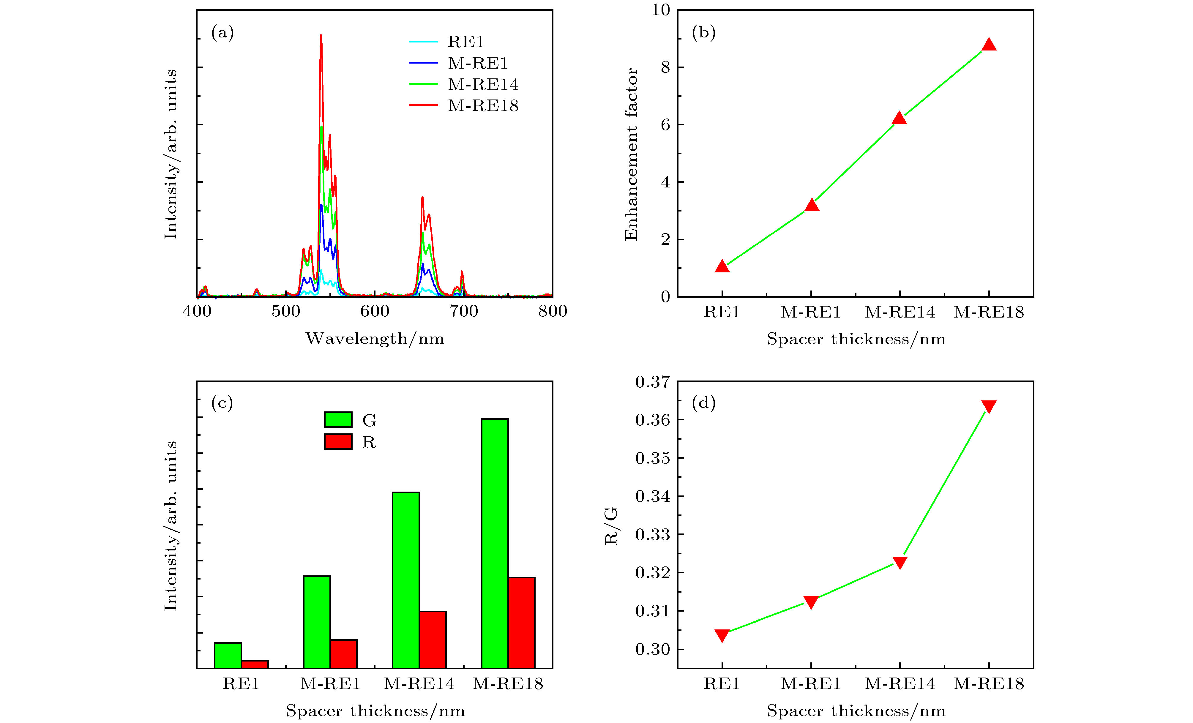
图 3 在980 nm激光激发下, (a)不同衬底的NaYF4:20%Yb3+/2%Er3+纳米晶体上转换发射光谱图; (b)对应的荧光增强因子; (c)和(d)随着衬底变化Er3+离子的发射峰面积及对应的R/G比值(RE1: NaYF4:20%Yb3+/2%Er3+; M-RE1, M-RE14和M-RE18: GVA@SiO2 (0, 4, 8 nm)@NaYF4: 20%Yb3+/2%Er3+)
Fig. 3. (a) and (b) Upconversion emission spectra and enhancement factor of different systems under 980 nm excitation; (c) and (d) the peak area of the green and red emission intensity and corresponding R/G ratio of the NaYF4:20%Yb3+/2%Er3+ with wafer and different thicknesses of isolation layer about from 0 to 8 nm (RE1: NaYF4: 20%Yb3+/2%Er3+; M-RE1, M-RE14 and M-RE18: GVA@SiO2 (0, 4, 8 nm)@NaYF4: 20%Yb3+/2%Er3+).
图 4 在980 nm激光激发下, (a)不同衬底的NaYF4:40%Yb3+/2%Er3+纳米晶体上转换发光光谱图; (b)对应的发光增强倍数; (c)和(d)随着衬底变化Er3+离子的发射峰面积及对应的R/G比值(RE2: NaYF4:40%Yb3+/2%Er3+; M-RE2, M-RE24和M-RE28: GVA@SiO2 (0, 4, 8 nm)@NaYF4:40%Yb3+/2%Er3+)
Fig. 4. (a) and (b) Upconversion emission spectra and enhancement factor of different systems under 980 nm excitation; (c) and (d) the peak area of the green and red emission intensity and corresponding R/G ratio of the NaYF4:40%Yb3+/2%Er3+ with wafer and different thicknesses of isolation layer about from 0 to 8 nm (RE2: NaYF4:40%Yb3+/2%Er3+; M-RE2, M-RE24, and M-RE28: GVA@SiO2 (0, 4, 8 nm)@NaYF4:40%Yb3+/2%Er3+).
图 6 在980 nm激发光下, (a) GVA@SiO2 (8 nm)@NaYF4:40%Yb3+/2%Er3+纳米体系上转换发光光谱图; (b), (c) GVA@SiO2 (8 nm)@NaYF4:40%Yb3+/2%Er3+上转换发射强度和光谱的红绿比与其激发功率之间的关系
Fig. 6. (a) Upconversion emission spectra of GVA@SiO2 (8 nm)@NaYF4:40%Yb3+/2%Er3+ nanocrystals; (b) and (c) are graphs corresponding to the emission intensity and the red-green ratio as a function of the 980 nm laser excitation power from 40 mW to 160 mW.
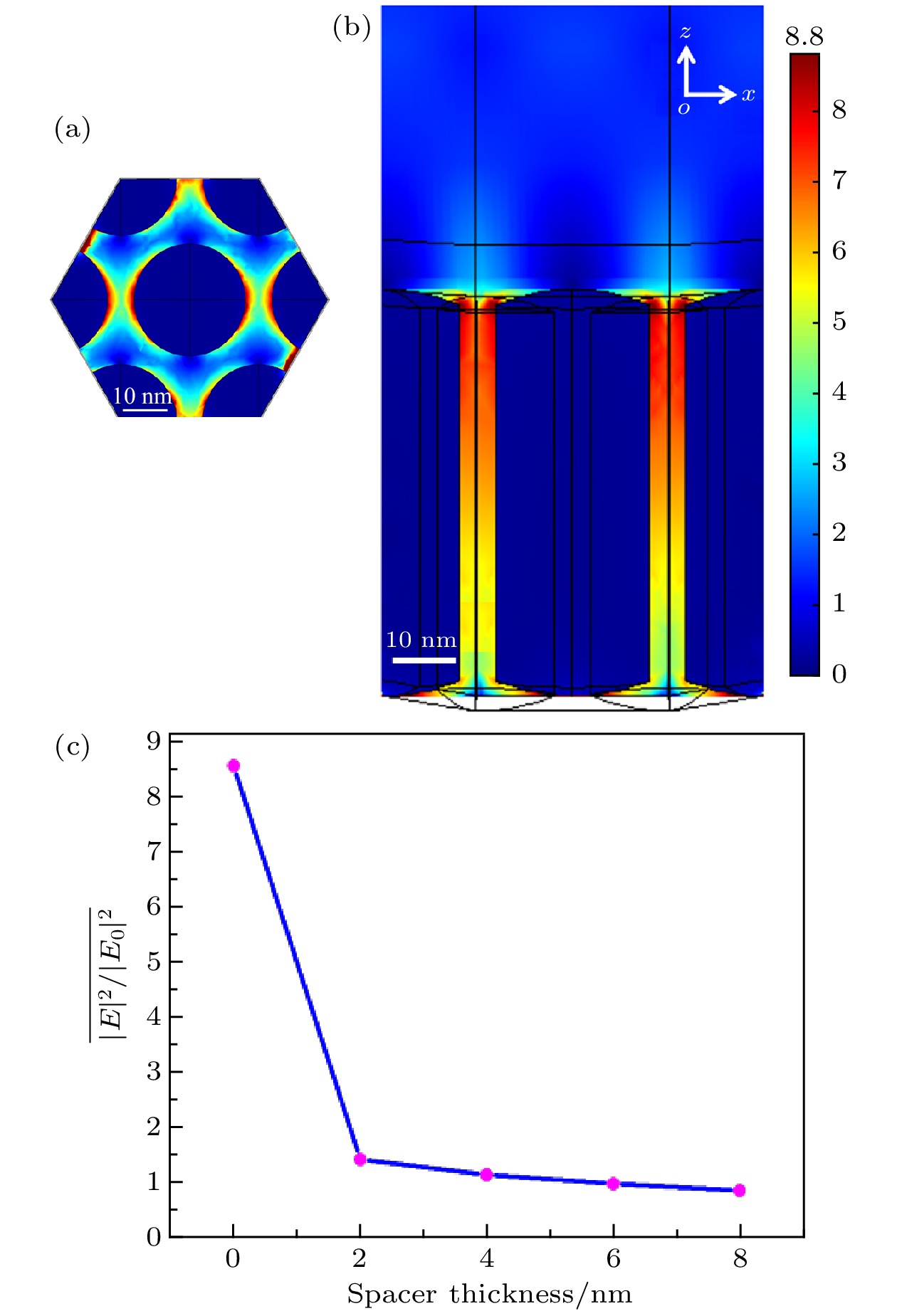
图 8 在980 nm激发光下, 模拟了GVA@SiO2结构最小单元的局部电磁场分布 (a) x-y平面的局域电磁场分布图; (b) GVA@SiO2 (2 nm)的x-z截面局域电磁场分布图; (c) SiO2厚度的变化与其上表面由局域等离激元效应产生的局域电磁场热点强度变化图
Fig. 8. Local electromagnetic field distribution of the smallest unit of the GVA@SiO2 system is simulated under 980 nm excitation: (a) The local electromagnetic field distribution map of the x-y plane; (b) the GVA@SiO2 (2 nm) of x-z cross-section local electromagnetic field distribution diagram was illustrated; (c) the intensity of the localized electromagnetic field hot spot produced by the LSPR with the SiO2 thickness changed.
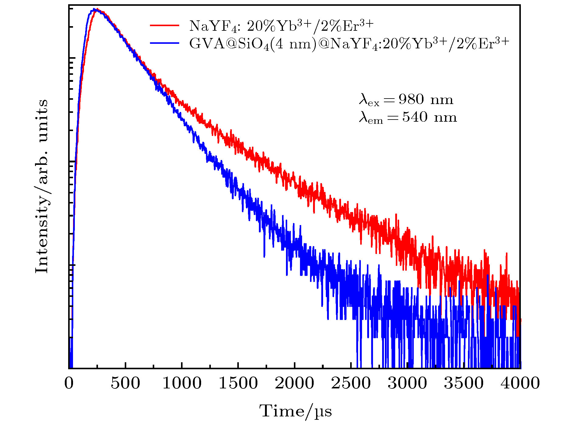
表 1 980 nm脉冲激发光激发下GVA@SiO2@NaYF4:20%Yb3+/2%Er3+复合体系中Er3+离子的4S3/2能级辐射寿命
Table 1. Luminescence lifetimes of 4S3/2 energy level (540 nm) in GVA@SiO2@NaYF4: 20%Yb3+/2%Er3+ composite system under 980 nm pulse laser excitation.
Sample Lifetime/μs (540 nm) a: NaYF4:20%Yb3+/2%Er3+ 361.945 ± 1.681 b: AuNRs Array/NaYF4:20%Yb3+/2%Er3+ 358.005 ± 1.679 c: AuNRs array/4 nm SiO2/NaYF4:20%Yb3+/2%Er3+ 342.060 ± 1.571 d: AuNRs array/8 nm SiO2/NaYF4:20%Yb3+/2%Er3+ 212.075 ± 0.892 -
[1] Runowski M, Stopikowska N, Szeremeta D, Goderski S, Skwierczyńska M, Lis S 2019 ACS. Appl. Mat. Inter. 11 13389
 Google Scholar
[2] Hassan A M, Wu X, Jarrett J W, et al. 2019 Biomed. Opt. Express 10 584
 Google Scholar
[3] Zhou B, Shi B Y, Jin D Y, Liu X G 2015 Nat. Nanotechnol. 10 924
 Google Scholar
[4] Wang M, Li M, Yu A, Wu J, Mao C 2015 ACS. Appl. Mat. Inter. 7 28110
 Google Scholar
[5] Gong G, Song Y, Tan H H, Xie S W, Zhang C F, Xu L J, Xu J X, Zheng J 2019 Compos. Part B-Eng. 179 107504
 Google Scholar
[6] Chen G Y, Damasco J, Qiu H L, et al. 2015 Nano. Lett. 15 7400
 Google Scholar
[7] 何恩节, 郑海荣, 高伟, 等 2013 62 237803
 Google Scholar
He E J, Zheng H R, Gao W, et al. 2013 Acta Phys. Sin. 62 237803
 Google Scholar
[8] Dong J, Zhang J, Han Q, Zhao X, Yan X W, Liu J H, Ge H B, Gao W 2019 J. Lumin. 207 361
 Google Scholar
[9] Dong J, Gao W, Han Q, Wang Y K, Qia J X, Yan X W, Sun M T 2018 Rev. Math. Phys. 4 100026
 Google Scholar
[10] 韩庆艳, 高伟, 祁建霞, 张成云, 赵星, 张正龙, 董军, 郑海荣 2018 中国科学: 物理学 力学 天文学 48 82
 Google Scholar
Han Q Y, Gao W, Qi J X, Zhang C Y, Zhao X, Zhang Z L, Dong J, Zheng H R 2018 Sci. Sin-Phys. Mech. Astron. 48 82
 Google Scholar
[11] Dong J, Zhang Z L, Zheng H R, Sun M T 2015 Nanophotonics-Berlin 4 472
 Google Scholar
[12] Park W, Lu D W, Ahn S 2015 Chem. Soc. Rev. 44 2940
 Google Scholar
[13] Feng W, Sun L D, Yan C H 2009 Chem. Commun. 29 4393
 Google Scholar
[14] Dong J, Zhao X, Cao E, et al. 2020 Mater. Today 9 100067
 Google Scholar
[15] Clarke C, Liu D, Wang F, e al. 2018 Nanoscale 10 6270
 Google Scholar
[16] Wang Q R, Zhang J, Sang X, Zhang D, Shi Q, Li S H, Wang W J 2018 J. Lumin. 204 284
 Google Scholar
[17] Zong H, Mu X J, Sun M T 2019 Appl. Mater. Today 15 43
 Google Scholar
[18] Das A, Mao C C, Cho S, Kim K, Park W 2018 Nat. Commun. 9 4828
 Google Scholar
[19] He E J, Yu J J, Wang C, Jiang Y, Zuo X Z, Xu B, Wen J, Qin Y F, Wang Z J 2020 Mater. Res. Bull. 121 110613
 Google Scholar
[20] Xu W, Chen X, Song H W 2017 Nano. Today 17 54
 Google Scholar
[21] Ji Y N, Xu W, Li D Y, Zhou D L, Chen X, Ding N, Li J, Wang N, Bai X, Song H W 2019 Nano. Energy 61 211
 Google Scholar
[22] Yin Z, Zhou D L, Xu W, Cui S B, Chen X, Wang H, Xu S H, Song H W 2016 ACS. Appl. Mat. Inter. 8 11667
 Google Scholar
[23] Kang F W, He J J, Sun T Y, Bao Z Y, Wang F, Lei D Y 2017 Adv. Funct. Mater. 27 1701842
 Google Scholar
[24] Gao W, Wang B Y, Han Q Y, Gao L, Wang Z J, Sun Z Y, Zhang B, Dong J 2020 J. Alloy. Compd. 818 152934
 Google Scholar
[25] Nikoobakht B, El-Sayed M A 2003 Chem. Mater. 15 1957
 Google Scholar
[26] Dong J, Zhao X, Gao W, Han Q Y, Qi J X, Wang Y K, Guo S D, Sun M T 2019 Nanoscale. Res. Lett. 14 118
 Google Scholar
[27] Man X K, D oi, M 2016 Phys Rev Lett, 116 066101
 Google Scholar
[28] Gao W, Kong X Q, Han Q Y, et al. 2018 J. Lumin. 196 187
 Google Scholar
[29] 高伟, 董军 2017 66 204206
 Google Scholar
Gao W, Dong J 2017 Acta Phys. Sin. 66 204206
 Google Scholar
[30] Liu X, Lei D Y 2015 Sci. Rep-Uk. 5 15235
 Google Scholar
[31] Rohani S, Quintanilla M, Tuccio S, et al. 2015 Adv. Opt. Mater. 3 1606
 Google Scholar
[32] Wang T, Siu C K, Yu H, et al. 2018 Inorg. Chem. 57 8200
 Google Scholar
[33] Saboktakin M, Ye X C, Oh S J, et al. 2012 ACS Nano 6 8758
 Google Scholar
[34] Feng A L, You M L, Tian L M, Singamaneni S, Lin M, Duan Z F, Lu T J, Xu F, Lin M 2015 Sci. Rep-Uk. 5 7779
 Google Scholar
[35] Green K, Wirth J, Lim S F 2016 Nanotechnology 27 135201
 Google Scholar
[36] 严学文, 王朝晋, 王博扬, 等 2019 68 174204
 Google Scholar
Yan X W, Wang Z J, Wang B Y, et al. 2019 Acta Phys. Sin. 68 174204
 Google Scholar
[37] Elrafei S A, Kandas I, Shehata N, Samir E, Okaz A, Rizk M 2018 J. Lumin. 204 581
 Google Scholar
[38] Schietinger S, Aichele T, Wang H Q, Nann T, Benson O 2009 Nano Lett. 10 134
 Google Scholar
[39] Saboktakin M, Ye X C, Chettiar U K, Engheta N, Murray C B, Kagan C R 2013 ACS Nano 7 7186
 Google Scholar
[40] Zhao X, Dong J, Cao E, Han Q Y, Gao W, Wang Y K, Qi J X, Sun M T 2019 Appl. Mater. Today 14 166
 Google Scholar
[41] Jung K 2019 B Korean Chem. Soc. 40 91
 Google Scholar
计量
- 文章访问数: 13106
- PDF下载量: 207
- 被引次数: 0


 下载:
下载:
