


-
实现对量子隧穿电阻的精确调控, 是铁电隧道结技术迈向应用的核心瓶颈. 本研究提出了一种基于界面功函数工程的策略, 其核心在于利用铁电极化翻转, 主动调控异质结界面的能带对齐, 从而在势垒层中诱导出可逆的金属-绝缘体相变, 实现对隧穿电阻的调控. 以Al2Te3/In2Se3范德瓦耳斯异质结为研究对象, 通过第一性原理计算证明, 对界面功函数的策略性调控可在势垒层中诱导出可逆的金属-绝缘体转变, 从而显著地改变其隧穿电阻. 非平衡输运模拟进一步显示, 该结构实现了高达2.69×10⁵%的隧穿电阻比值. 研究结果不仅凸显了Al2Te3/In2Se3作为高性能铁电隧道结的潜力, 也为在低维铁电存储器件中设计超高隧穿电阻效应确定了一种普适的设计策略. 这项工作为开发多状态非易失性存储器提供了新的思路.In recent years, two-dimensional (2D) ferroelectric materials have attracted widespread interest due to their ultrathin geometry, high stability, and switchable polarization states. Ferroelectric tunnel junctions (FTJs) made from 2D ferroelectric materials exhibit exceptionally high tunnel electroresistance (TER) ratios, making them leading candidates for next-generation non-volatile memory and logic devices. However, advancing FTJ technology depends on overcoming the critical challenge of precisely controlling quantum tunneling resistance. Therefore, this study proposes a strategy of interfacial work function engineering, which actively modulates the band alignment of a heterostructure through ferroelectric polarization switching, induces a reversible metal-insulator transition in the barrier layer, and modulates TER. Using a van der Waals heterostructure composed of Al2Te3/In2Se3 as a model system, we demonstrate through first-principles calculations that the strategic manipulation of interfacial work functions can induce a reversible metal-insulator transition in the barrier, thereby drastically changing the tunneling conductance. Further analysis indicates that a work function mismatch between the two ferroelectric materials causes varying degrees of interfacial charge transfer, thereby triggering a metal-insulator transition in the van der Waals ferroelectric heterostructure as the external electric field is reversed. Non-equilibrium transport simulations reveal an unprecedented TER ratio of 2.69×10⁵%. Our findings not only highlight Al2Te3/In2Se3 as a promising platform for high-performance FTJs but also establish a universal design strategy for engineering ultrahigh TER effects in low-dimensional ferroelectric memory devices. This work opens new avenues for developing energy-efficient, non-volatile memory with enhanced scalability and switching characteristics.
-
Keywords:
- two-dimensional ferroelectric heterostructure /
- band modulation /
- polarization /
- first-principles calculations
-
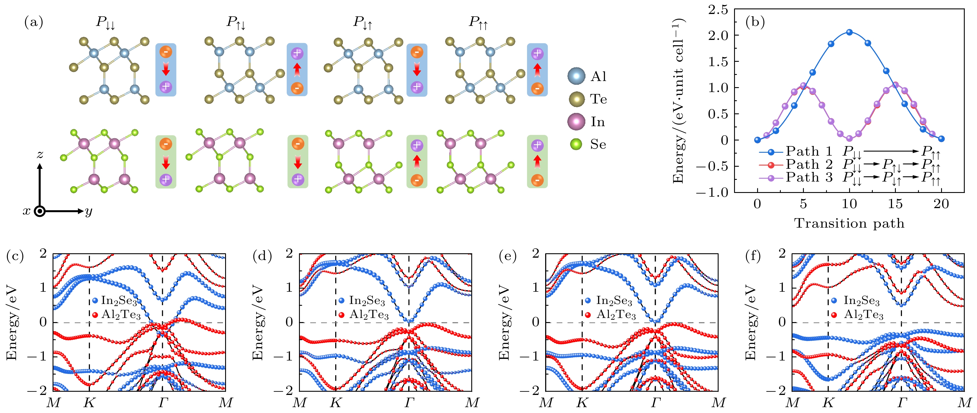
图 1 (a) Al2Te3/In2Se3异质结的四种堆叠方式的结构示意图; (b) 异质结从${P}_{\downarrow \downarrow } $到${P}_{\uparrow \uparrow } $的翻转路径. 异质结不同极化态的能带结构 (c) ${P}_{\downarrow \downarrow }$; (d) ${P}_{\uparrow \downarrow } $; (e) ${P}_{\downarrow \uparrow } $; (f) ${P}_{\uparrow \uparrow } $
Fig. 1. (a) Schematic representation of the four possible stacking states for Al2Te3/In2Se3 heterostructure. (b) The transition pathway between ${P}_{\downarrow \downarrow } $ and ${P}_{\uparrow \uparrow } $. The layer-projected band structures for the state: (c) ${P}_{\downarrow \downarrow } $, (d) ${P}_{\uparrow \downarrow } $, (e) ${P}_{\downarrow \uparrow } $, and (f) ${P}_{\uparrow \uparrow } $.
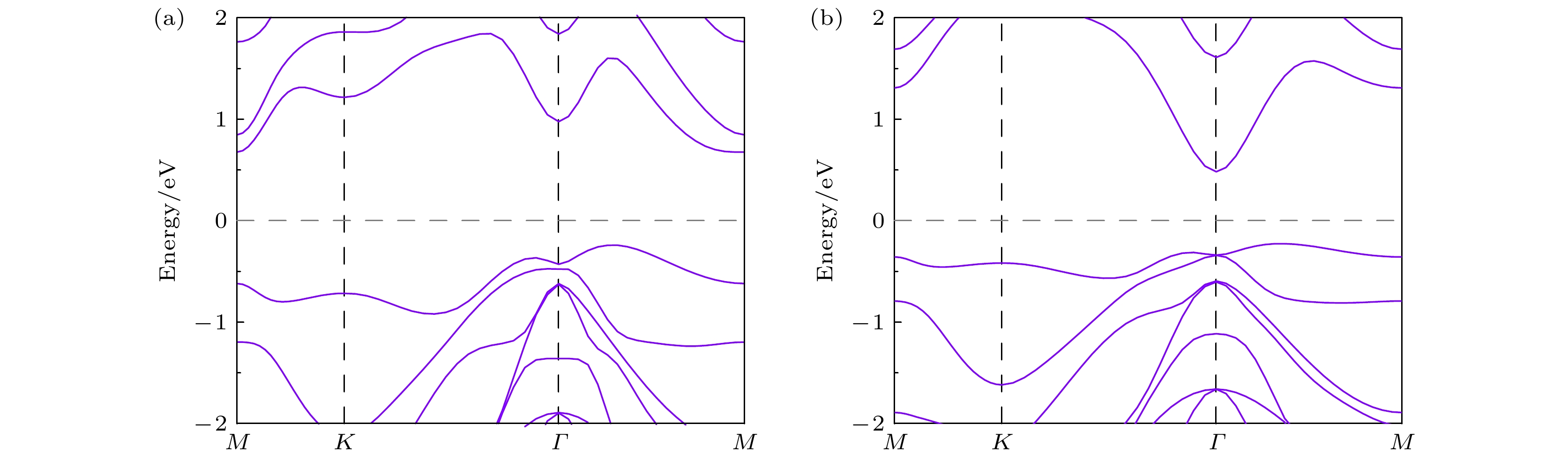
图 2 (a) Al2Te3和(b) In2Se3的能带结构
Fig. 2. The band structures of (a) Al2Te3 and (b) In2Se3.
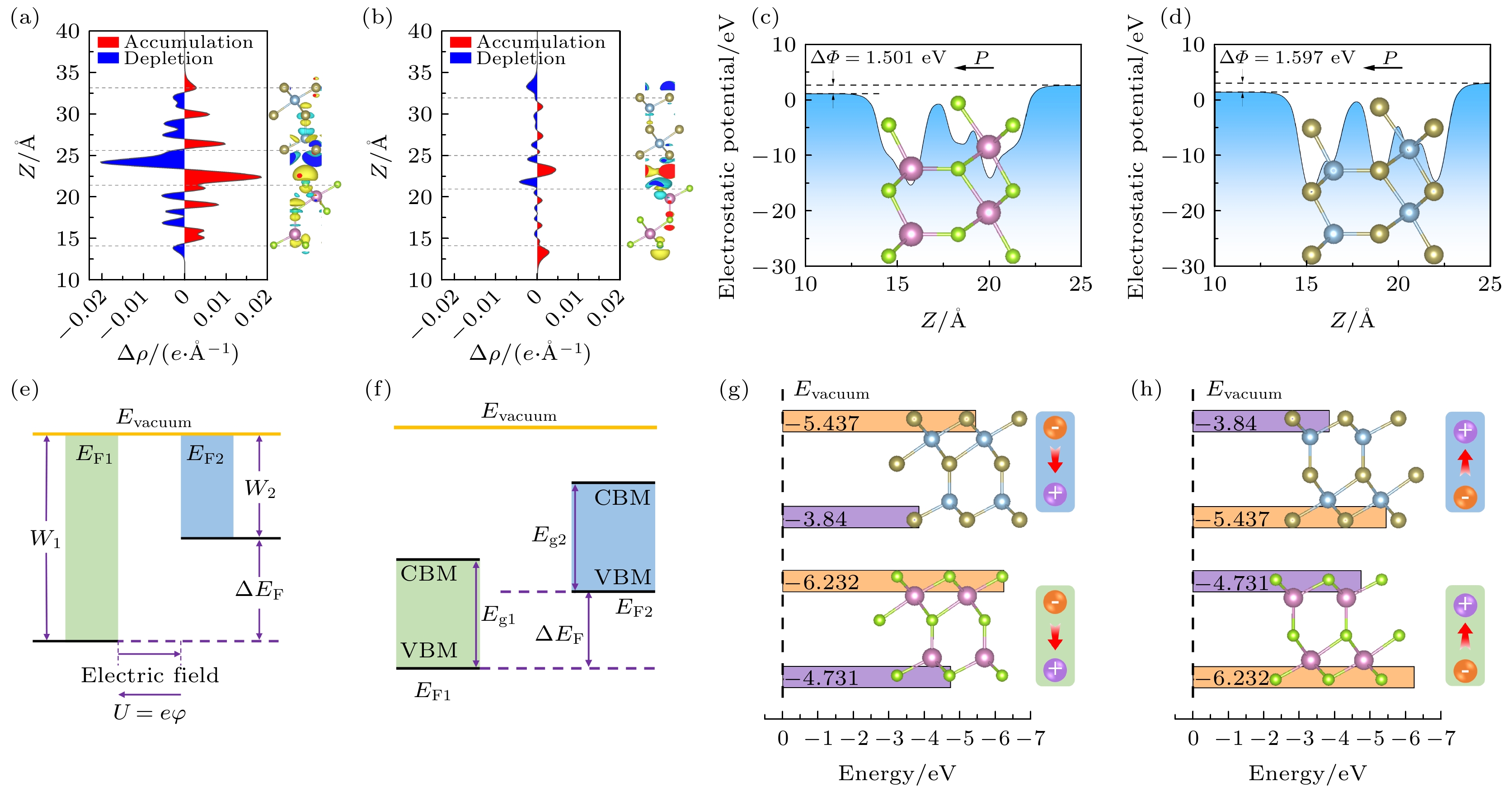
图 3 (a) ${P}_{\downarrow \downarrow } $极化态和(b) ${P}_{\uparrow \uparrow } $极化态下Al2Te3/In2Se3异质结沿z方向的平面平均电荷密度差; (c) In2Se3和(d) Al2Te3的静电势; (e) 异质结界面接触电势差形成机理示意图; (f) 两种半导体在接触前(达到平衡前)的能带对齐示意图; (g) ${P}_{\downarrow \downarrow } $极化态和(h) ${P}_{\uparrow \uparrow } $极化态下Al2Te3/In2Se3异质结中Al2Te3和In2Se3单层的功函数
Fig. 3. The differential charge density diagrams along the z direction of Al2Te3/In2Se3 heterostructures with (a) ${P}_{\downarrow \downarrow } $ and (b) ${P}_{\uparrow \uparrow } $ states; plane-averaged electrostatic potential of (c) In2Se3 and (d) Al2Te3; (e) schematic diagram of the formation of contact potential and (f) band alignment between two different materials for two-dimensional van der Waals heterostructure; the work functions of Al2Te3 and In2Se3 in the (g) ${P}_{\downarrow \downarrow } $ state and the (h) ${P}_{\uparrow \uparrow } $ state for Al2Te3/In2Se3 heterostructures.
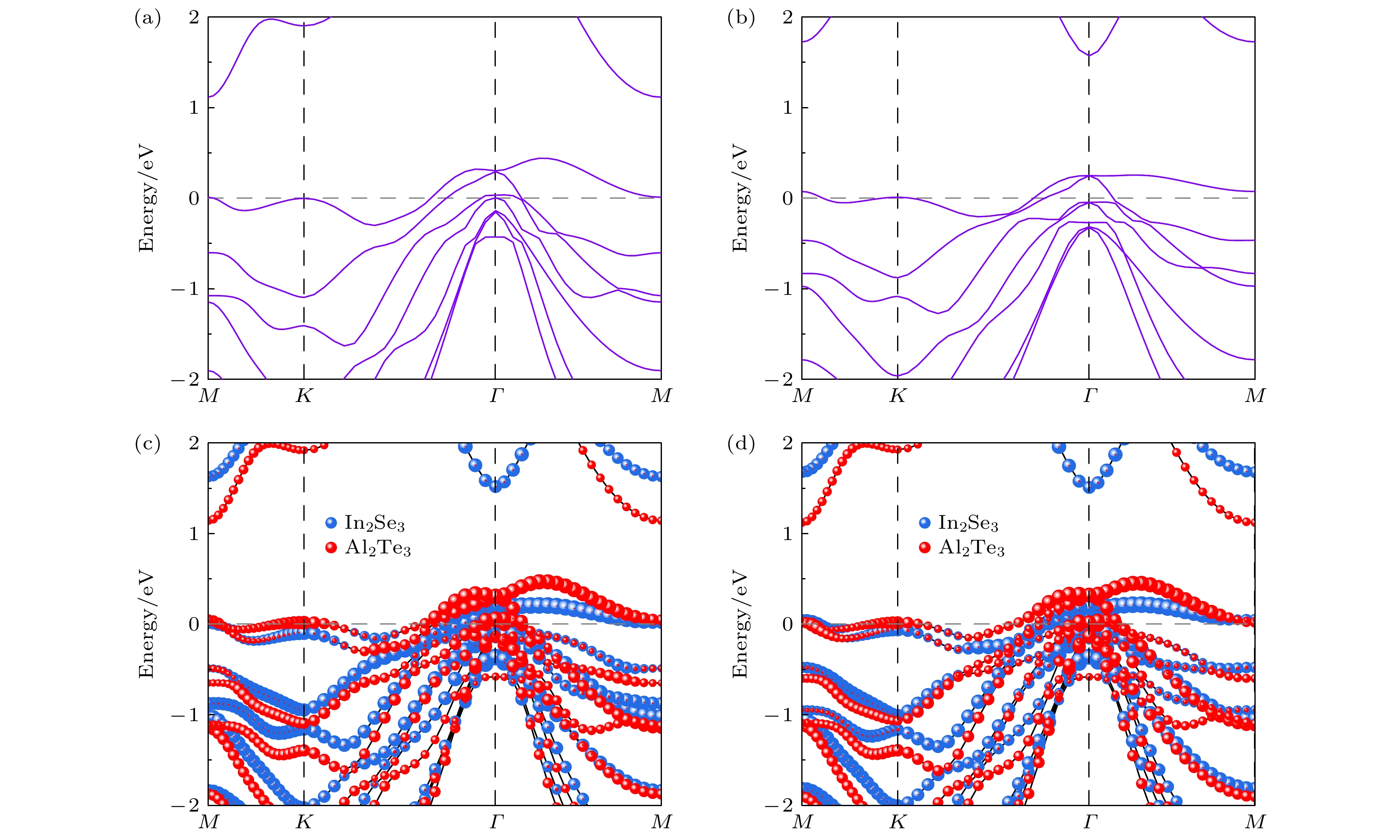
图 4 (a) Al2(Te0.5Sb0.5)3和(b) In2(Se0.5As0.5)3的能带结构; (c) ${P}_{\downarrow \downarrow } $极化态和(d) ${P}_{\uparrow \uparrow } $极化态下Al2(Te0.5Sb0.5)3/In2(Se0.5As0.5)3的能带结构
Fig. 4. The band structures of (a) Al2(Te0.5Sb0.5)3, (b) In2(Se0.5As0.5)3; the (c) ${P}_{\downarrow \downarrow } $ and (d) ${P}_{\uparrow \uparrow } $ state of Al2(Te0.5Sb0.5)3/In2(Se0.5As0.5)3 of.
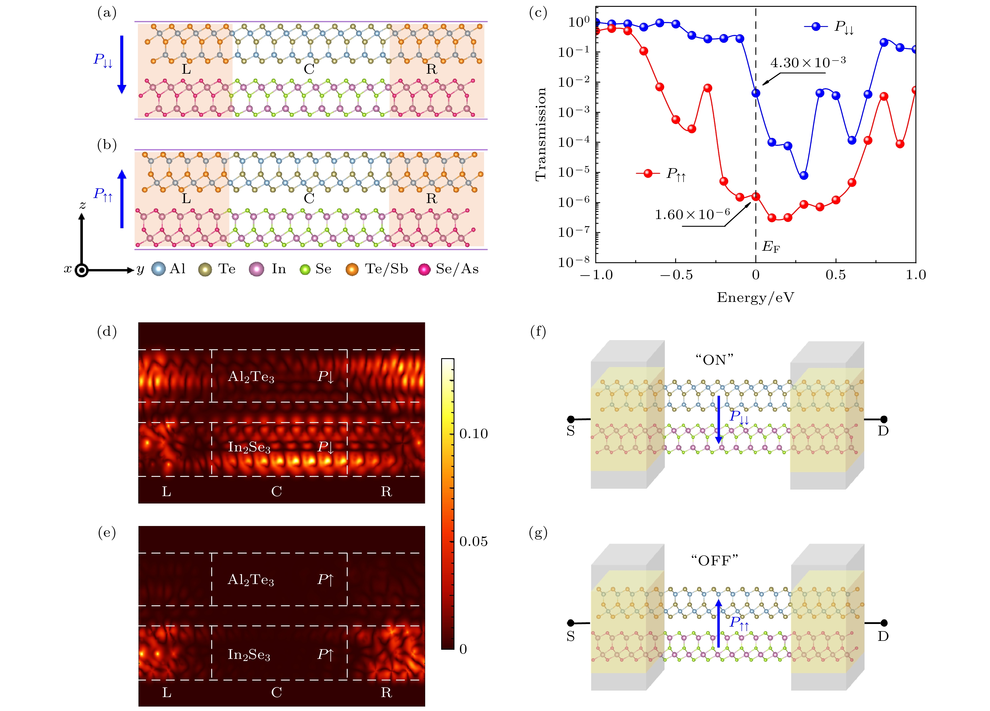
图 5 (a) ${P}_{\downarrow \downarrow } $极化态和(b) ${P}_{\uparrow \uparrow } $极化态下基于Al2Te3/In2Se3异质结的场效应晶体管的原子结构侧视图; (c) Al2Te3/In2Se3隧道结透射函数; 在费米能级处, (d) ${P}_{\downarrow \downarrow } $极化态和(e) ${P}_{\uparrow \uparrow } $极化态下基于Al2Te3/In2Se3异质结的场效应晶体管的散射态; 铁电隧道结原型器件结构 (f) “ON”态和(g) “OFF”态
Fig. 5. The side views of atomic structures of Al2Te3/In2Se3-based FTJs with N=7 for the (a) ${P}_{\downarrow \downarrow } $ and (b) ${P}_{\uparrow \uparrow } $ states. (c) The transmission function of the FTJs in ${P}_{\downarrow \downarrow } $ and ${P}_{\uparrow \uparrow } $ states as a function of energy. The scattering states at Fermi level for Al2Te3/In2Se3-based FTJs when N=7 for the (d) ${P}_{\downarrow \downarrow } $ and (e) ${P}_{\uparrow \uparrow } $ states. The (f) “ON” state and (g) “OFF” state of the device prototype for FTJs applications.
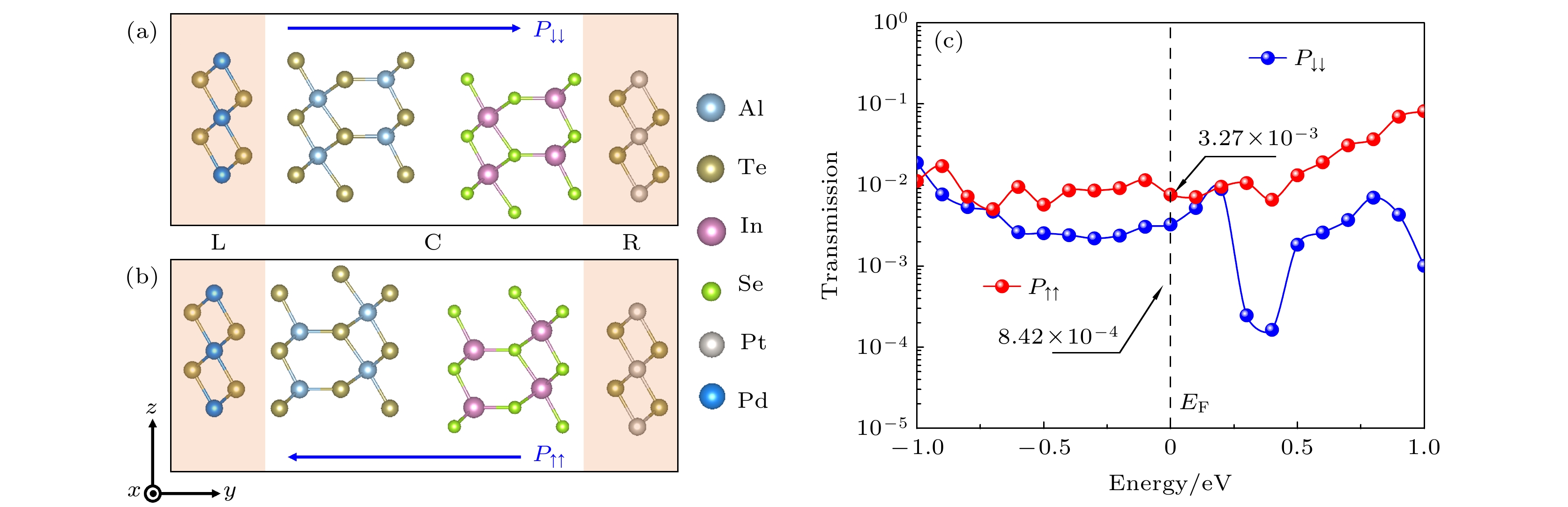
图 6 (a) $ {P}_{\downarrow \downarrow }$极化态和(b) ${P}_{\uparrow \uparrow } $极化态下基于PdTe2/Al2Te3/In2Se3/PtTe2的隧道结结构; (c) Al2Te3/In2Se3隧道结透射函数
Fig. 6. The atomic structures of PdTe2/Al2Te3/In2Se3/PtTe2-based FTJs for the (a) ${P}_{\downarrow \downarrow } $ and (b) ${P}_{\uparrow \uparrow } $ states; (c) the transmission function of the FTJs in ${P}_{\downarrow \downarrow } $ and ${P}_{\uparrow \uparrow } $ states as a function of energy.
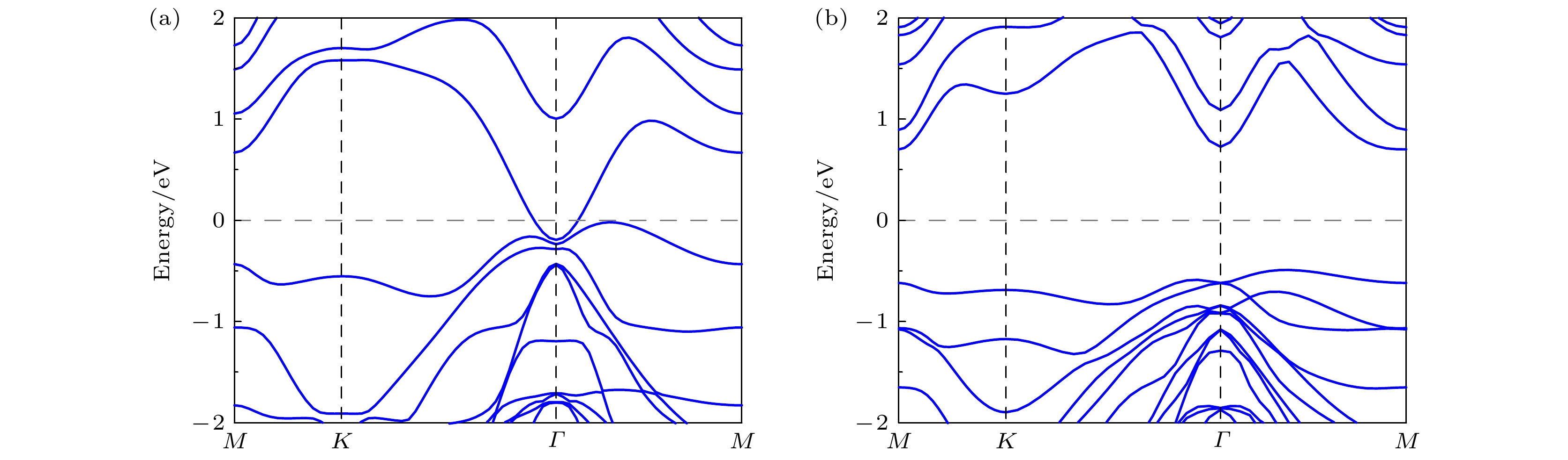
图 7 (a) ${P}_{\downarrow \downarrow } $极化态和(b) ${P}_{\uparrow \uparrow } $极化态下基于Heyd-Scuseria-Ernzerhof(HSE06)杂化泛函计算获得的Al2Te3/In2Se3异质结的能带结构
Fig. 7. The band structures of Al2Te3/In2Se3 heterostructure with HSE06 functional for the (a) ${P}_{\downarrow \downarrow } $ and (b) ${P}_{\uparrow \uparrow } $ state.
表 1 不同构型Al2Te3/In2Se3异质结的形成能
Table 1. Formation energy of Al2Te3/In2Se3 heterostructures with different configurations.
${P}_{\downarrow \downarrow } $ ${P}_{\uparrow \downarrow } $ ${P}_{\downarrow \uparrow } $ ${P}_{\uparrow \uparrow } $ 构型1(Te-In堆垛) –37.389 eV –37.352 eV –37.353 eV –37.358 eV 构型2(Te-Se堆垛) –37.378 eV –37.347 eV –37.352 eV –37.353 eV  下载: 导出CSV
-
[1] Luo K F, Ma Z, Sando D, Zhang Q, Valanoor N 2025 ACS Nano 19 6622
 Google Scholar
[2] Tsymbal E Y, Kohlstedt H 2006 Science 313 181
Google Scholar
[3] Zheng N, Li J, Sun H, Zang Y, Jiao P, Shen C, Jiang X, Xia Y, Deng Y, Wu D, Pan X, Nie Y 2025 Sci. Adv. 11 eads0724
Google Scholar
[4] Bai X, Zou D, Lei C, He Z, Liu Y 2025 Appl. Phys. Lett. 126 162902
Google Scholar
[5] Berdan R, Marukame T, Ota K, Yamaguchi M, Saitoh M, Fujii S, Deguchi J, Nishi Y 2020 Nat. Electron. 3 259
Google Scholar
[6] Zhuravlev M Y, Sabirianov R F, Jaswal S S, Tsymbal E Y 2005 Phys. Rev. Lett. 94 246802
Google Scholar
[7] Yu X, Zhang X, Ma L, Wang J 2024 Adv. Funct. Mater. 34 2409281
Google Scholar
[8] Kim D J, Lu H, Ryu S, Bark C W, Eom C B, Tsymbal E Y, Gruverman A 2012 Nano Lett. 12 5697
Google Scholar
[9] Li Y, Yang Y, Zhao H, Duan H, Yang C, Min T, Li T 2025 Nano Lett. 25 1680
Google Scholar
[10] Junquera J, Ghosez P 2003 Nature 422 506
Google Scholar
[11] Yang Q, Tao L, Zhang Y, Li M, Jiang Z, Tsymbal E Y, Alexandrov V 2019 Nano Lett. 19 7385
Google Scholar
[12] Jia Y, Yang Q, Fang Y W, Lu Y, Xie M, Wei J, Tian J, Zhang L, Yang R 2024 Nat. Commun. 15 693
Google Scholar
[13] Liu F, You L, Seyler K L, Li X, Yu P, Lin J, Wang X, Zhou J, Wang H, He H, Pantelides S T, Zhou W, Sharma P, Xu X, Ajayan P M, Wang J, Liu Z 2016 Nat. Commun. 7 12357
Google Scholar
[14] Qi J, Han H, Yang S, Kang L, Yin H, Zhao G 2024 Appl. Phys. Lett. 125 042903
Google Scholar
[15] Ding W, Zhu J, Wang Z, Gao Y, Xiao D, Gu Y, Zhang Z, Zhu W 2017 Nat. Commun. 8 14956
Google Scholar
[16] Zheng C, Yu L, Zhu L, Collins J L, Kim D, Lou Y, Xu C, Li M, Wei Z, Zhang Y, Edmonds M T, Li S, Seidel J, Zhu Y, Liu J Z, Tang W X, Fuhrer M S 2018 Sci. Adv. 4 eaar7720
Google Scholar
[17] Kim C, Moon I, Lee D, Choi M S, Ahmed F, Nam S, Cho Y, Shin H J, Park S, Yoo W J 2017 ACS Nano 11 1588
Google Scholar
[18] Popov I, Seifert G, Tománek D 2012 Phys. Rev. Lett. 108 156802
Google Scholar
[19] Liu Z, Hou P, Sun L, Tsymbal E Y, Jiang J, Yang Q 2023 npj Comput. Mater. 9 6
Google Scholar
[20] Xie A, Hao H, Liu C S, Zheng X, Zhang L, Zeng Z 2023 Phys. Rev. B 107 115427
Google Scholar
[21] 李景辉, 曹胜果, 韩佳凝, 李占海, 张振华 2024 73 137102
Google Scholar
Li J H, Cao S G, Han J N, Li Z H, Zhang Z H 2024 Acta Phys. Sin. 73 137102
Google Scholar
[22] 李永宁, 谢逸群, 王音 2021 70 227701
Google Scholar
Li Y N, Xie Y Q, Wang Y 2021 Acta Phys. Sin. 70 227701
Google Scholar
[23] Kresse G, Furthmüller J 1996 Phys. Rev. B 54 11169
Google Scholar
[24] Kresse G, Joubert D 1999 Phys. Rev. B 59 1758
[25] Kresse G, Furthmüller J 1996 Comput. Mater. Sci. 6 15
Google Scholar
[26] Blöchl P E 1994 Phys. Rev. B 50 17953
Google Scholar
[27] Grimme S 2006 J. Comput. Chem. 27 1787
Google Scholar
[28] Vydrov O A, Heyd J, Krukau A V, Scuseria G E 2006 J. Chem. Phys. 125 074106
Google Scholar
[29] Taylor J, Guo H, Wang J 2001 Phys. Rev. B 63 245407
Google Scholar
[30] Monkhorst H J, Pack J D 1976 Phys. Rev. B 13 5188
Google Scholar
[31] Soni R, Petraru A, Meuffels P, Vavra O, Ziegler M, Kim S K, Jeong D S, Pertsev N A, Kohlstedt H 2014 Nat. Commun. 5 5414
Google Scholar
[32] Chen Y, Guo J T, Li M X, Wang G Z, Yuan H K, Chen H 2024 Surf. Interfaces 51 104597
Google Scholar
[33] Fu C-F, Sun J, Luo Q, Li X, Hu W, Yang J 2018 Nano Lett. 18 6312
Google Scholar
[34] Fan A, Zhang Q, Yang Z, Li L, Li M, Zhang K, Gao J, Wu F, Wu M, Geng D, Hu W 2025 Sci. Adv. 11 eadx8192
Google Scholar
[35] Meng P, Wu Y, Bian R, Pan E, Dong B, Zhao X, Chen J, Wu L, Sun Y, Fu Q, Liu Q, Shi D, Zhang Q, Zhang Y W, Liu Z, Liu F 2022 Nat. Commun. 13 7696
Google Scholar
[36] Ding J, Shao D F, Li M, Wen L W, Tsymbal E Y 2021 Phys. Rev. Lett. 126 057601
Google Scholar
[37] Lu H L, Yang M, Xie Z Y, Geng Y, Zhang Y, Wang P F, Sun Q Q, Ding S J, Wei Zhang D 2014 Appl. Phys. Lett. 104 161602
Google Scholar
[38] Fang Z, Solovyev I V, Terakura K 2000 Phys. Rev. Lett. 84 3169
Google Scholar


 下载:
下载:


计量
- 文章访问数: 464
- PDF下载量: 7
- 被引次数: 0
