


-
GaN基肖特基势垒二极管(SBD)器件具有功率密度高、转换效率高以及开关特性好等优点. GaN材料在异质外延过程中不可避免地会引入大量的位错, 而位错会导致器件的可靠性问题. 本文报道了一种在自支撑GaN衬底上生长并制备的超低位错密度N+/N– GaN 准垂直SBD器件. 高分辨X射线衍射仪和原子力显微镜表征结果显示, 在自支撑GaN衬底上实现了总位错密度为1.01 × 108 cm–2, 表面均方根粗糙度为0.149 nm的高质量外延层的生长. 基于高质量外延层制备的器件在不使用任何终端、场板以及等离子体处理的情况下, 在反向电压为–5 V时表现出10–5 A/cm2的极低泄漏电流密度, 与在蓝宝石衬底上同步制备的对照组器件相比, 反向泄漏电流低4个数量级. 实验结果表明, 基于自支撑GaN衬底的准垂直GaN基SBD能够大幅度降低器件的反向漏电, 极大地提升准垂直SBD器件的电学性能. 使用微光显微镜对两组器件进行观察, 确定了准垂直SBD器件的泄漏电流主要集中在阳极边缘, 并解释了漏电机理. 最后对器件进行了变温测试, 在温度为100 ℃时, 仍表现出低于10–3 A/cm3的泄漏电流, 证明了自支撑GaN衬底上准垂直SBD器件具有优良的应用前景.
-
关键词:
- 自支撑GaN /
- 位错密度 /
- 准垂直型肖特基二极管 /
- 电学性能
GaN based Schottky barrier diode (SBD) possesses advantages including high power density, high conversion efficiency, and excellent switching characteristics. During heteroepitaxial growth of GaN, a high density of threading dislocations is inevitably introduced, which can degrade device reliability. This paper reports a low dislocation density N+/N– GaN quasi-vertical SBD fabricated on a freestanding GaN substrate. The characterization results of high-resolution X-ray diffraction and atomic force microscopy demonstrate that the high-quality epitaxial layer with a total dislocation density of 1.01 × 108 cm–2 and a root mean square surface roughness of 0.149 nm is achieved on a freestanding GaN substrate. The device prepared based on a high-quality epitaxial layer exhibits an ultra-low leakage current density of 10–5 A/cm2 at a reverse voltage of –5 V, without employing any edge termination structures or field plates or plasma treatment. Compared with the devices prepared on sapphire substrates using identical processes, the device prepared in this work reduces the reverse leakage current by four orders of magnitude. The experimental results show that the quasi-vertical GaN based SBD fabricated on a freestanding GaN substrate significantly reduces reverse leakage current and substantially enhances the overall electrical performance of the device. By employing emission-microscope (EMMI), leakage current in quasi-vertical SBD is identified to be primarily localized at the anode edge, and the underlying leakage mechanism is elucidated. Finally, temperature-dependent measurements demonstrate that the device maintains a leakage current below 10–3 A/cm2 at 100 ℃, confirming the potential of quasi-vertical SBD on freestanding GaN substrate for practical applications.-
Keywords:
- freestanding GaN /
- dislocation density /
- quasi-vertical schottky diode /
- electrical properties
[1] Liu X, Xu S R, Zhang T, Tao H C, Su H K, Gao Y, Xie L, Wang X H, Zhang J C, Hao Y 2025 Appl. Phys. Lett. 126 202103
 Google Scholar
[2] 徐爽, 许晟瑞, 王心颢, 卢灏, 刘旭, 贠博祥, 张雅超, 张涛, 张进成, 郝跃 2023 72 196101
Google Scholar
Xu S, Xu S R, Wang X H, Lu H, Liu X, Yun B X, Zhang Y C, Zhang T, Zhang J C, Hao Y 2023 Acta Phys. Sin. 72 196101
Google Scholar
[3] Su H K, Xu S R, Tao H C, Fan X M, Du J J, Peng R S 2021 IEEE Electron Device Lett. 10 1109
[4] 许钪, 许晟瑞, 陶鸿昌, 苏华科, 高源, 杨赫, 安暇, 黄俊, 张进成, 郝跃 2024 电子学报 52 3907
Xu K, Xu S R, Tao H C, Su H K, Gao Y, Yang H, An X, Huang J, Zhang J C, Hao Y 2024 Acta Electron. Sin. 52 3907
[5] Su H K, Zhang T, Xu S R, Tao H C, Gao Y, Liu X, Xie L, Xiang P, Cheng K, Hao Y, Zhang J C 2024 Appl. Phys. Lett. 124 162102
Google Scholar
[6] Tan G H, Yan F, Chen X L, Luo W K 2018 Appl. Opt. 10 1364
[7] Brendel M, Helbling M, Knigge A, Brunner F, Weyers M 2015 Electron. Lett. 51 1598
Google Scholar
[8] Zhang Y, Wong H Y, Sun M, Joglekar S, Yu L, Braga N A 2015 IEDM 10 1109
Google Scholar
[9] Jin W Y, Zhang Y M, Xia S Y, Zhu Q Z, Sun Y H, Yi J M, Wang J F, Xu K 2024 AIP Adv. 14 095118
Google Scholar
[10] Xu J Y, Liu X, Xie B, Hao Y L, Wen C P, Wei J 2023 IEEE Trans. Electron. Device 32 41260
[11] Liao Y Q, Chen T, Wang J, Cai W T, Ando Y, Yang X, Watanabe H, Tanaka A 2022 Appl. Phys. Lett. 120 122109
Google Scholar
[12] Yoshizumi Y, Hashimoto S, Tanabe T, Kiyama M 2007 J. Cryst. Growth 298 8758
Google Scholar
[13] Ban K, Yamamoto J, Takeda K, Ide K, Iwaya M, Takeuchi T, Kamiyama S, Akasaki I, Amano H 2011 Appl. Phys. Express 4 052101
Google Scholar
[14] Lu H, Xu S R, Huang Y, Chen X, Xu S, Liu X, Wang X H, Gao Y, Zhang Y C, Duan X L, Zhang J C, H Y 2024 J. Inorg. Mater. 202 30490
Google Scholar
[15] Lu X, Liu C, Jiang H X, Zou X B, Zhang A P, Lau K M 2016 Appl. Phys. Express 9 031001
Google Scholar
[16] Li Q B, Liu G X, Wang S Z, Liu L, Yu J X, Wang G D, Cui P, Zhang S Y, Xu X G, Zhang L 2025 Surf. Interfaces 56 105554
Google Scholar
[17] Liu W S, Wu S H, Balaji G, Huang L C, Chi C K, Hu K J, Kuo H C 2024 Appl. Phys. A 130 801
Google Scholar
[18] 武鹏, 张涛, 张进成, 郝跃 2022 71 158503
Google Scholar
Wu P, Zhang T, Zhang J C, Hao Y 2022 Acta Phys. Sin. 71 158503
Google Scholar
[19] Cao Y, Chu R, Li R, Chen M, Chang R, Hughes B 2016 Appl. Phys. Lett 108 062103
Google Scholar
[20] Chen J B, Bian Z K, Liu Z H, Ning J, Duan X L, Zhao S L, Wang H Y, Tang Q, Wu Y H, Song Y Q, Zhang J C, Hao Y 2019 Semicond. Sci. Technol. 34 115019
Google Scholar
[21] Lambert D J H, Zhu T G, Shelton B S, Wong M M, Chowdhury U, Dupuis R D 2000 Appl. Phys. Lett. 77 2918
Google Scholar
[22] Witte W, Fahle D, Koch H, Heuken M, Kalisch H, Vescan A 2012 Semicond. Sci. Technol 27 085015
Google Scholar
[23] Zhang Y H, Sun M, Piedra D, Azize M, Zhang X, Fujishima T 2014 IEEE Trans. Electron Devices 10 1109
[24] Bian Z K, Zhou H, Xu S R, Zhang T, Dang K, Chen J B, Zhang J C, Hao Y 2019 Superlattices Microstruct. 125 295
Google Scholar
[25] Tokuda H, Watanabe F, Syahiman A, Kuzuhara M, Fujiwara T 2011 IEEE MTT-S 10 1109
Google Scholar
[26] Li L, Kishi A, Liu Q, Itai Y, Fujihara R, Ohno Y 2014 IEEE J. Electron Devices Soc. 6 168
[27] Sang L W, Ren B, Sumiya M, Liao M, Koide Y 2017 Appl. Phys. Lett. 111 122102
Google Scholar
[28] Kim B, Moon D, Joo K, Oh S, Lee Y K, Park Y, Nanishi Y, Yoon E 2014 Appl. Phys. Lett. 104 102101
Google Scholar
[29] Wang J, You H F, Guo H, Xue J J, Yang G F, Chen D J, Liu B, Lu H, Zhang R, Zheng Y D 2020 Appl. Phys. Lett. 116 062104
Google Scholar
-
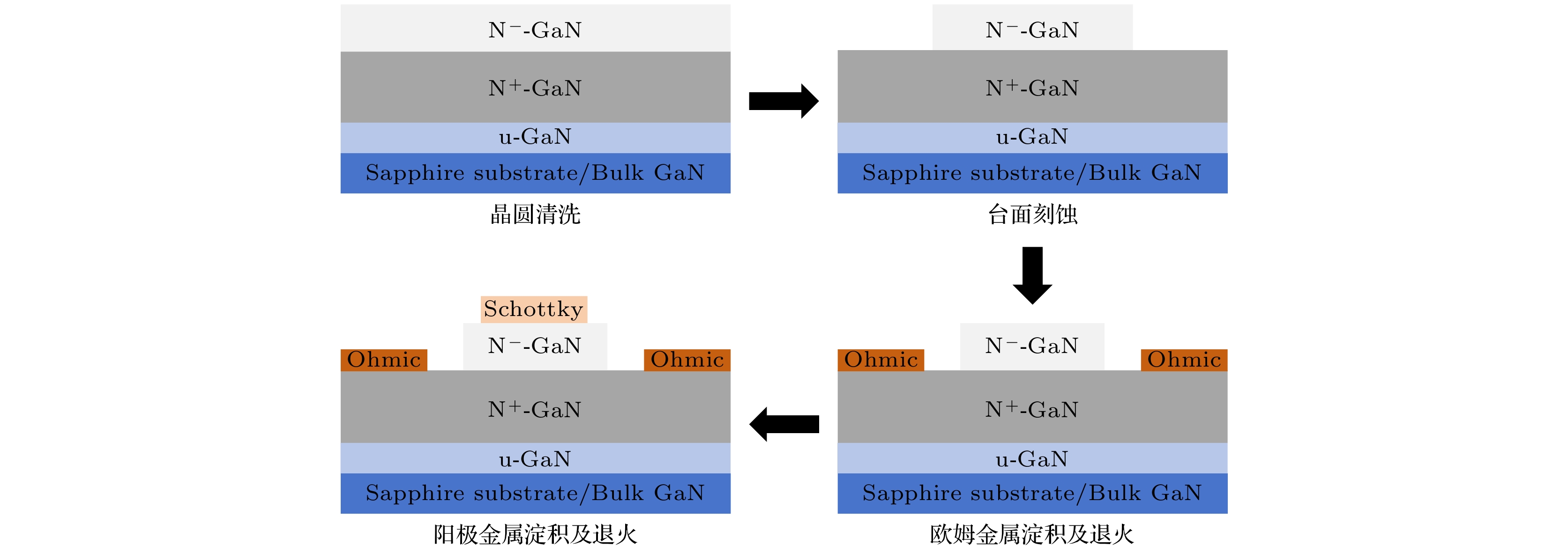
图 1 准垂直GaN SBD器件的制备工艺流程图
Fig. 1. Preparation process flow chart of quasi vertical GaN SBD device.
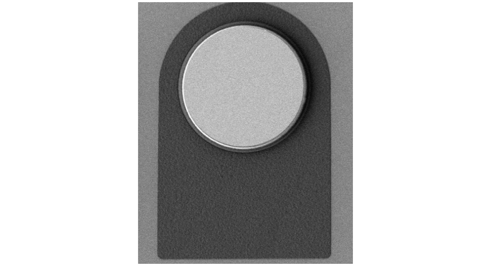
图 2 准垂直结构GaN SBD器件的SEM图
Fig. 2. SEM image of GaN SBD device with quasi vertical structure.
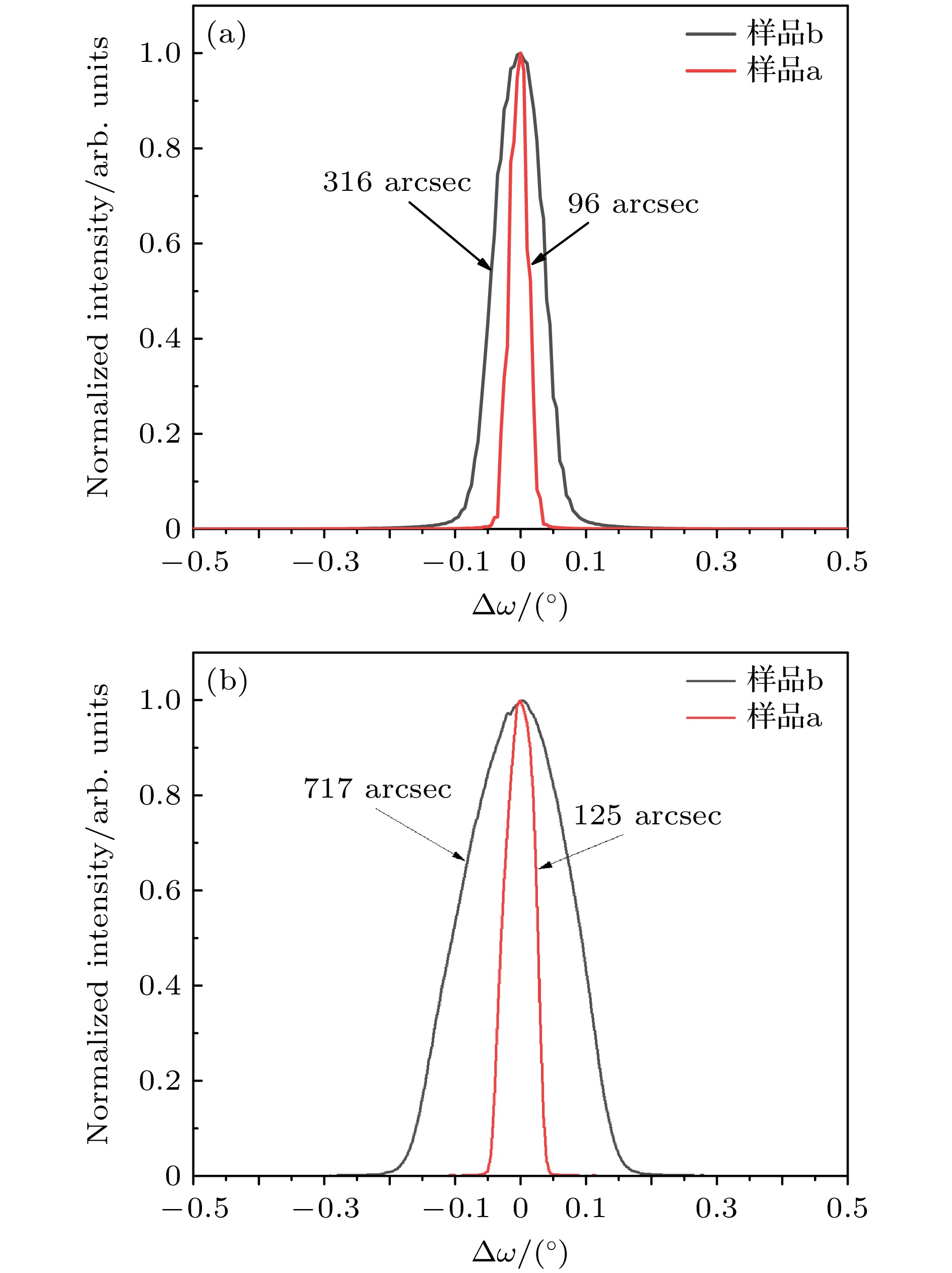
图 3 样品a和样品b的(002)面(a)和(102)面(b)的XRD摇摆曲线图
Fig. 3. XRD rocking curves of (002) plane (a) and (102) plane (b) of samples a and b.
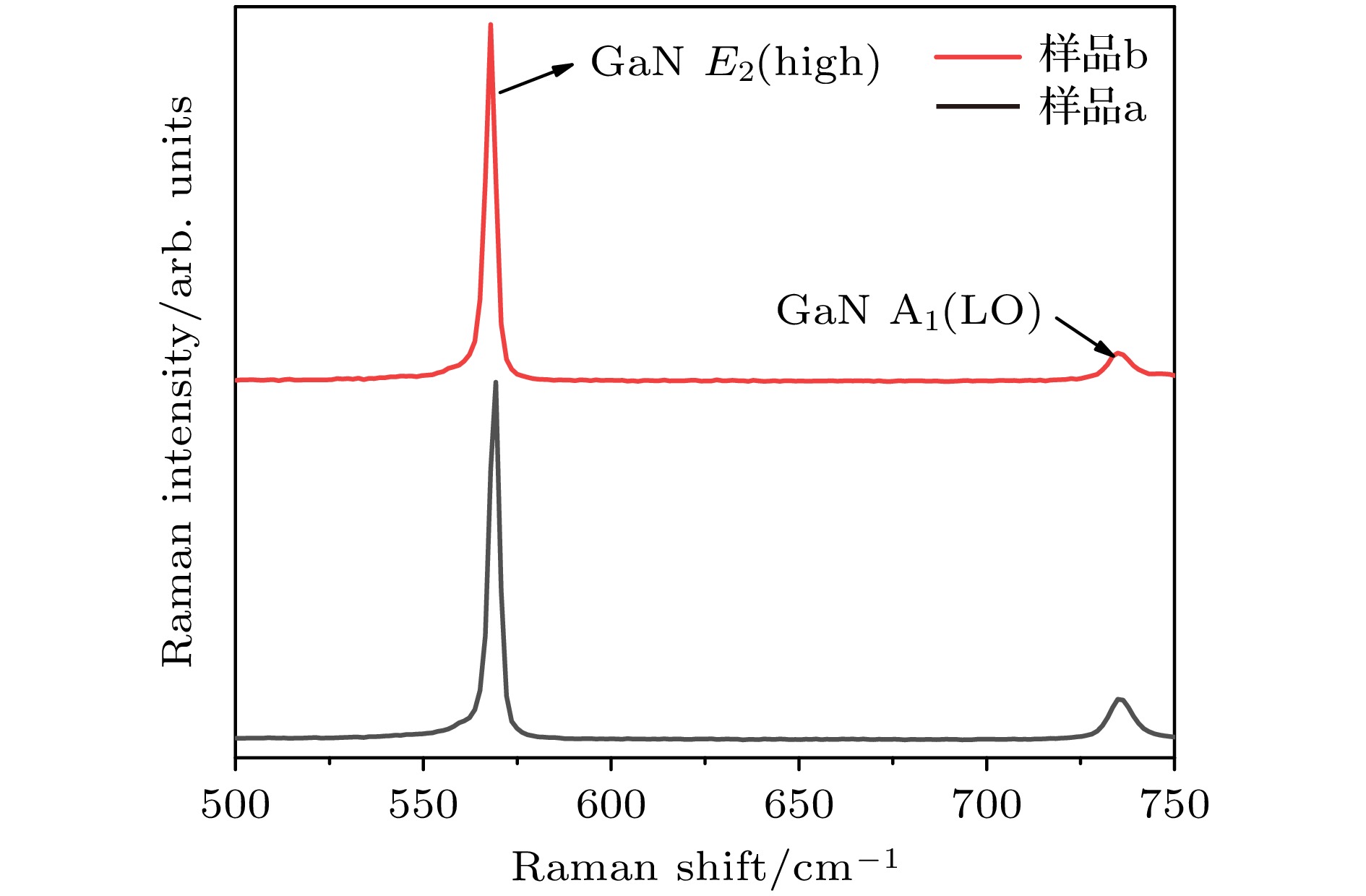
图 5 样品a和样品b室温下Raman图
Fig. 5. Raman spectra of sample a and sample b at room temperature.
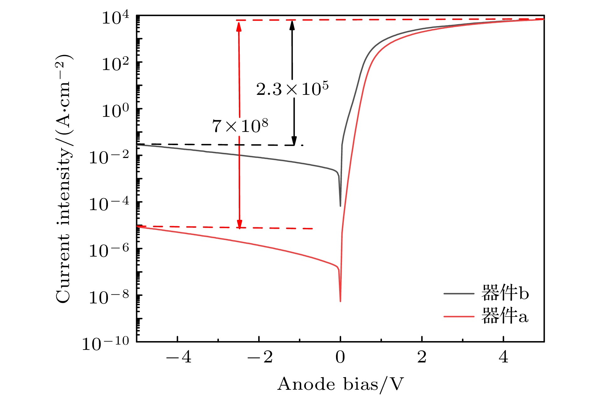
图 6 器件a和器件b在半对数坐标下的正反向I-V曲线
Fig. 6. Forward and reverse I-V curves of device a and device b in semi-logarithmic coordinates.
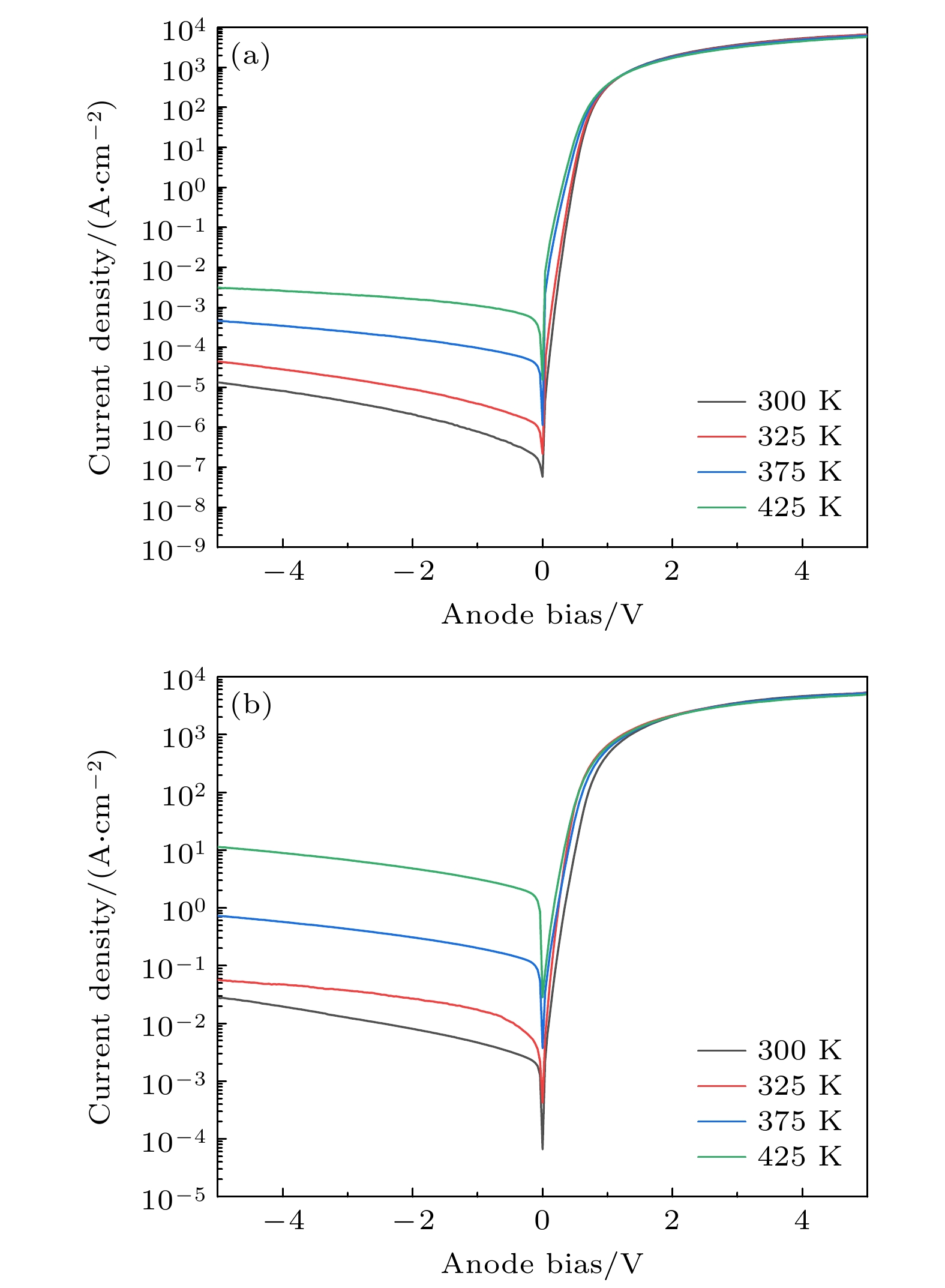
图 8 半对数坐标下器件a (a)和器件b (b)正反向I-V特性随温度的变化关系
Fig. 8. Forward and backward I-V characteristics of device a (a) and device b (b) with temperature in semi-logarithmic coordinates.
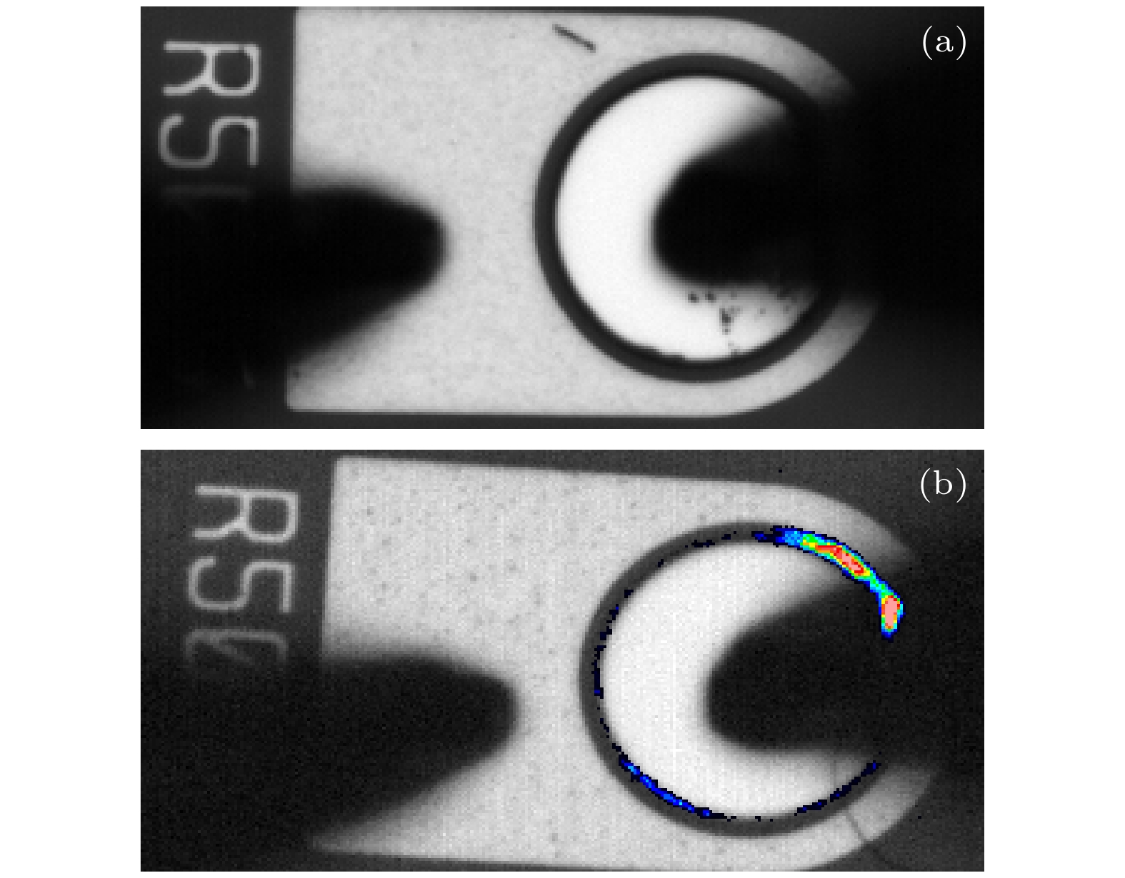
图 9 反向偏压10 V下器件a (a)和器件b (b)的EMMI图
Fig. 9. EMMI images of device a (a) and device b (b) under reverse bias of 10 V.
表 1 两组样品在(002)和(102)晶面的半高宽和位错密度
Table 1. FWHM and dislocation density of two groups of samples on the (002) and (102) crystal plane.
编号 (002)/
arcsec(102)/
arcsec螺位错密
度/cm–2刃位错密
度/cm–2总位错密
度/cm–2样品a 96 125 1.85×10⁷ 8.28×10⁷ 1.01×10⁸ 样品b 319 717 2.04×10⁸ 2.73×10⁹ 2.93×10⁹  下载: 导出CSV
-
[1] Liu X, Xu S R, Zhang T, Tao H C, Su H K, Gao Y, Xie L, Wang X H, Zhang J C, Hao Y 2025 Appl. Phys. Lett. 126 202103
Google Scholar
[2] 徐爽, 许晟瑞, 王心颢, 卢灏, 刘旭, 贠博祥, 张雅超, 张涛, 张进成, 郝跃 2023 72 196101
Google Scholar
Xu S, Xu S R, Wang X H, Lu H, Liu X, Yun B X, Zhang Y C, Zhang T, Zhang J C, Hao Y 2023 Acta Phys. Sin. 72 196101
Google Scholar
[3] Su H K, Xu S R, Tao H C, Fan X M, Du J J, Peng R S 2021 IEEE Electron Device Lett. 10 1109
[4] 许钪, 许晟瑞, 陶鸿昌, 苏华科, 高源, 杨赫, 安暇, 黄俊, 张进成, 郝跃 2024 电子学报 52 3907
Xu K, Xu S R, Tao H C, Su H K, Gao Y, Yang H, An X, Huang J, Zhang J C, Hao Y 2024 Acta Electron. Sin. 52 3907
[5] Su H K, Zhang T, Xu S R, Tao H C, Gao Y, Liu X, Xie L, Xiang P, Cheng K, Hao Y, Zhang J C 2024 Appl. Phys. Lett. 124 162102
Google Scholar
[6] Tan G H, Yan F, Chen X L, Luo W K 2018 Appl. Opt. 10 1364
[7] Brendel M, Helbling M, Knigge A, Brunner F, Weyers M 2015 Electron. Lett. 51 1598
Google Scholar
[8] Zhang Y, Wong H Y, Sun M, Joglekar S, Yu L, Braga N A 2015 IEDM 10 1109
Google Scholar
[9] Jin W Y, Zhang Y M, Xia S Y, Zhu Q Z, Sun Y H, Yi J M, Wang J F, Xu K 2024 AIP Adv. 14 095118
Google Scholar
[10] Xu J Y, Liu X, Xie B, Hao Y L, Wen C P, Wei J 2023 IEEE Trans. Electron. Device 32 41260
[11] Liao Y Q, Chen T, Wang J, Cai W T, Ando Y, Yang X, Watanabe H, Tanaka A 2022 Appl. Phys. Lett. 120 122109
Google Scholar
[12] Yoshizumi Y, Hashimoto S, Tanabe T, Kiyama M 2007 J. Cryst. Growth 298 8758
Google Scholar
[13] Ban K, Yamamoto J, Takeda K, Ide K, Iwaya M, Takeuchi T, Kamiyama S, Akasaki I, Amano H 2011 Appl. Phys. Express 4 052101
Google Scholar
[14] Lu H, Xu S R, Huang Y, Chen X, Xu S, Liu X, Wang X H, Gao Y, Zhang Y C, Duan X L, Zhang J C, H Y 2024 J. Inorg. Mater. 202 30490
Google Scholar
[15] Lu X, Liu C, Jiang H X, Zou X B, Zhang A P, Lau K M 2016 Appl. Phys. Express 9 031001
Google Scholar
[16] Li Q B, Liu G X, Wang S Z, Liu L, Yu J X, Wang G D, Cui P, Zhang S Y, Xu X G, Zhang L 2025 Surf. Interfaces 56 105554
Google Scholar
[17] Liu W S, Wu S H, Balaji G, Huang L C, Chi C K, Hu K J, Kuo H C 2024 Appl. Phys. A 130 801
Google Scholar
[18] 武鹏, 张涛, 张进成, 郝跃 2022 71 158503
Google Scholar
Wu P, Zhang T, Zhang J C, Hao Y 2022 Acta Phys. Sin. 71 158503
Google Scholar
[19] Cao Y, Chu R, Li R, Chen M, Chang R, Hughes B 2016 Appl. Phys. Lett 108 062103
Google Scholar
[20] Chen J B, Bian Z K, Liu Z H, Ning J, Duan X L, Zhao S L, Wang H Y, Tang Q, Wu Y H, Song Y Q, Zhang J C, Hao Y 2019 Semicond. Sci. Technol. 34 115019
Google Scholar
[21] Lambert D J H, Zhu T G, Shelton B S, Wong M M, Chowdhury U, Dupuis R D 2000 Appl. Phys. Lett. 77 2918
Google Scholar
[22] Witte W, Fahle D, Koch H, Heuken M, Kalisch H, Vescan A 2012 Semicond. Sci. Technol 27 085015
Google Scholar
[23] Zhang Y H, Sun M, Piedra D, Azize M, Zhang X, Fujishima T 2014 IEEE Trans. Electron Devices 10 1109
[24] Bian Z K, Zhou H, Xu S R, Zhang T, Dang K, Chen J B, Zhang J C, Hao Y 2019 Superlattices Microstruct. 125 295
Google Scholar
[25] Tokuda H, Watanabe F, Syahiman A, Kuzuhara M, Fujiwara T 2011 IEEE MTT-S 10 1109
Google Scholar
[26] Li L, Kishi A, Liu Q, Itai Y, Fujihara R, Ohno Y 2014 IEEE J. Electron Devices Soc. 6 168
[27] Sang L W, Ren B, Sumiya M, Liao M, Koide Y 2017 Appl. Phys. Lett. 111 122102
Google Scholar
[28] Kim B, Moon D, Joo K, Oh S, Lee Y K, Park Y, Nanishi Y, Yoon E 2014 Appl. Phys. Lett. 104 102101
Google Scholar
[29] Wang J, You H F, Guo H, Xue J J, Yang G F, Chen D J, Liu B, Lu H, Zhang R, Zheng Y D 2020 Appl. Phys. Lett. 116 062104
Google Scholar


 下载:
下载:


计量
- 文章访问数: 1444
- PDF下载量: 46
- 被引次数: 0
