


-
高输出功率密度下的热积累问题是氮化镓基功率器件面临的关键瓶颈之一. 纳米晶金刚石钝化层策略在GaN基高功率器件散热方面发挥着重要的作用. 在硅基AlGaN/GaN异质结材料上制备了厚420—440 nm、晶粒尺寸330—380 nm的纳米晶金刚石薄膜, 制备了纳米晶金刚石钝化的GaN基横向肖特基二极管器件, 并对比研究了其与SiNx钝化器件的电学、热学性质. 测试结果显示, 在直流偏置下, 有无纳米晶钝化层的二极管器件正向特性基本一致; 在–20 V偏置电压下, 对两种器件施加2.5 V脉冲电压后, 纳米晶钝化二极管电流密度仅退化2.6%, 而SiNx钝化器件电学特性几乎完全退化, 表明纳米晶金刚石钝化二极管具有对电流崩塌现象优异的抑制能力; 在变直流功率条件下对两种器件的热成像显微观测结果显示, 发生热损毁时, SiNx钝化器件输出功率密度约4 W/mm, 而纳米晶钝化器件则约为7.5 W/mm. 本文是纳米晶金刚石钝化工艺在GaN基功率二极管散热应用的首次报道, 充分证明了该策略在GaN基功率二极管方面的应用潜力.Thermal accumulation under high output power density is one of the key bottlenecks faced by GaN-based power devices. The nanocrystalline diamond (NCD) passivation layer strategy plays a crucial role in improving heat dissipation in high-power GaN devices, while the existing studies focus on GaN-based HEMT. In this study, nanocrystalline diamond films with a thickness of 380–450 nm are grown on Si-based AlGaN/GaN heterostructure materials using a microwave plasma chemical vapor deposition (MPCVD) system. Consequently, lateral Schottky barrier diode devices with NCD passivation are fabricated, and their electrical and thermal properties are investigated. The results show that the DC forward characteristics of the NCD passivated diodes are essentially the same as those of devices without NCD passivation. Moreover, dynamic voltage tests indicate that the NCD passivation layer significantly mitigates current collapse in GaN devices at high frequencies. Under a –20 V DC bias and a pulse voltage of 2.5 V, the current density degradation of NCD passivated devices is only 2.6%, whereas devices without diamond passivation almost completely degrade. Thermal imaging microscopy under varying DC power levels shows that thermal failure occurs at an output power density of approximately 4 W/mm for conventional devices, while NCD passivated devices can reach around 7.5 W/mm. The electrical degradation behaviour of NCD passivated device is also tested under long-time reverse bias. This work demonstrates for the first time the application of nanocrystalline diamond passivation to thermal management of GaN-based power diodes, and clearly demonstrates the potential of this strategy in non-HEMT power device applications.
-
Keywords:
- nanocrystalline diamond /
- GaN /
- diode /
- heat dissipation
[1] Bader S J, Lee H, Chaudhuri R, Huang S M, Hickman A, Molnar A, Xing H L G, Jena D, Then H W, Chowdhury N, Palacios T 2020 IEEE Trans. Electron Devices 67 4010
 Google Scholar
[2] Qin Y, Albano B, Spencer J, Lundh J S, Wang B, Buttay C, Tadjer M, DiMarino C, Zhang Y H 2023 J. Phys. D: Appl. Phys 56 093001
Google Scholar
[3] Minoura Y, Ohki T, Okamoto N, Sato M, Ozaki S, Yamada A, Kotani J 2022 Appl. Phys. Express 15 036501
Google Scholar
[4] Ding Y J, Li J Y, Hao Z L, Wang Q, Zhang H J, Peng Y, Chen M X 2024 IEEE Photonics Technol. Lett. 36 1005
Google Scholar
[5] Gerrer T, Pomeroy J, Yang F Y, Francis D, Carroll J, Loran B, Witkowski L, Yarborough M, Uren M J, Kuball M 2021 IEEE Trans. Electron Devices 68 1530
Google Scholar
[6] Malakoutian M, Kasperovich A, Rich D, Woo K, Perez C, Soman R, Saraswat D, Kim J K, Noshin M, Chen M, Vaziri S, Bao X Y, Shih C C, Woon W Y, Asheghi M, Goodson K E, Liao S S, Mitra S, Chowdhury S 2023 Cell Rep. Phys. Sci. 4 101686
Google Scholar
[7] Wang Y N, Hu X F, Ge L, Liu Z H, Xu M S, Peng Y, Li B, Yang Y Q, Li S Q, Xie X J, Wang X W, Xu X G, Hu X B 2023 Crystals 13 500
Google Scholar
[8] Rossi S, Alomari M, Zhang Y, Bychikhin S, Pogany D, Weaver J M R, Kohn E 2013 Diamond Relat. Mater. 40 69
Google Scholar
[9] Matsumae T, Kurashima Y, Takagi H, Shirayanagi Y, Hiza S, Nishimura K, Higurashi E 2022 Scr. Mater. 215 114725
Google Scholar
[10] Gao R H, Wang X H, Mu F W, Li X J, Wei C, Zhou W, Shi J A, Tian Y, Xing X J, Li H Y, Huang S, Jiang Q M, Wei K, Liu X Y 2024 J. Alloys Compd. 985 174075
Google Scholar
[11] Tadjer M J, Anderson T J, Ancona M G, Raad P E, Komarov P, Bai T, Gallagher J C, Koehler A D, Goorsky M S, Francis D A, Hobart K D, Kub F J 2019 IEEE Electron Device Lett. 40 881
Google Scholar
[12] 白玲, 宁静, 张进成, 王东, 王博宇, 武海迪, 赵江林, 陶然, 李忠辉 2023 人工晶体学报 52 901
Google Scholar
Bai L, Ning J, Zhang J C, Wang D, Wang B Y, Wu H D, Zhao J L, Tao R, Li Z H 2023 J. Synth. Cryst. 52 901
Google Scholar
[13] Gu Y, Zhang Y, Hua B, Ni X, Fan Q, Gu X 2021 J. Electron. Mater. 50 4239
Google Scholar
[14] 兰飞飞, 刘莎莎, 房诗舒, 王英民, 程红娟 2024 人工晶体学报 53 913
Google Scholar
Lan F F, Liu S S, Fang S S, Wang Y M, Cheng H J 2024 J. Synth. Cryst. 53 913
Google Scholar
[15] Zheng Y T, Li C M, Liu J L, Wei J J, Ye H T 2021 Funct. Diamond 1 63
Google Scholar
[16] Yang H, Ma Y, Dai Y 2021 Funct. Diamond 1 150
Google Scholar
[17] Anderson T J, Hobart K D, Tadjer M J, Koehler A D, Imhoff E A, Hite J K, Feygelson T I, Pate B B, Eddy C R, Kub F J 2016 ECS J. Solid State Sci. Technol. 6 Q3036
Google Scholar
[18] Guo H, Li Y, Yu X, Zhou J, Kong Y 2022 Micromachines (Basel) 13 1486
Google Scholar
[19] Zhou X Y, Malakoutian M, Soman R, Bian Z L, Martinez R P, Chowdhury S 2022 IEEE Trans. Electron Devices 69 6650
Google Scholar
[20] 刘庆彬, 蔚翠, 郭建超, 马孟宇, 何泽召, 周闯杰, 高学栋, 余浩, 冯志红 2023 72 098104
Google Scholar
Liu Q B, Yu C, Guo J C, Ma M Y, He Z Z, Zhou C J, Gao X D, Yu H, Feng Z H 2023 Acta Phys. Sin. 72 098104
Google Scholar
[21] Ryou J H, Choi S 2022 Nat. Electron. 5 834
Google Scholar
[22] Tadjer M J, Anderson T J, Hobart K D, Feygelson T I, Caldwell J D, Eddy C R, Kub F J, Butler J E, Pate B, Melngailis J 2012 IEEE Electron. Device Lett. 33 23
Google Scholar
[23] Meyer D J, Koehler A D, Hobart K D, Eddy C R, Feygelson T I, Anderson T J, Roussos J A, Tadjer M J, Downey B P, Katzer D S, Pate B B, Ancona M G 2014 IEEE Electron. Device Lett. 35 1013
Google Scholar
[24] Johnstone D, Doğan S, Leach J, Moon Y T, Fu Y, Hu Y, Morkoç H 2004 Appl. Phys. Lett. 85 4058
Google Scholar
-
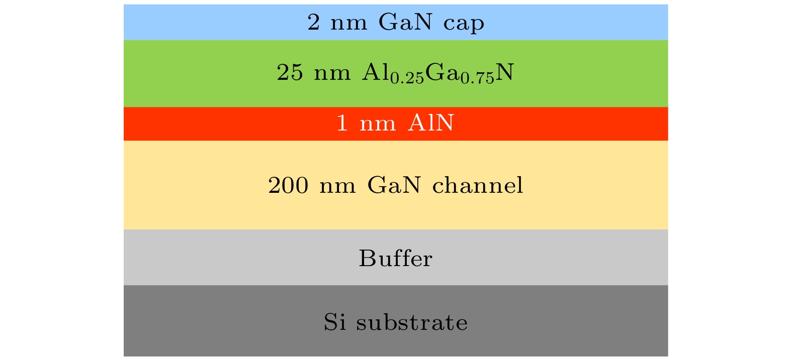
图 1 Si基AlGaN/GaN异质结外延片结构
Fig. 1. Si-based AlGaN/GaN heterojunction epitaxial structure.
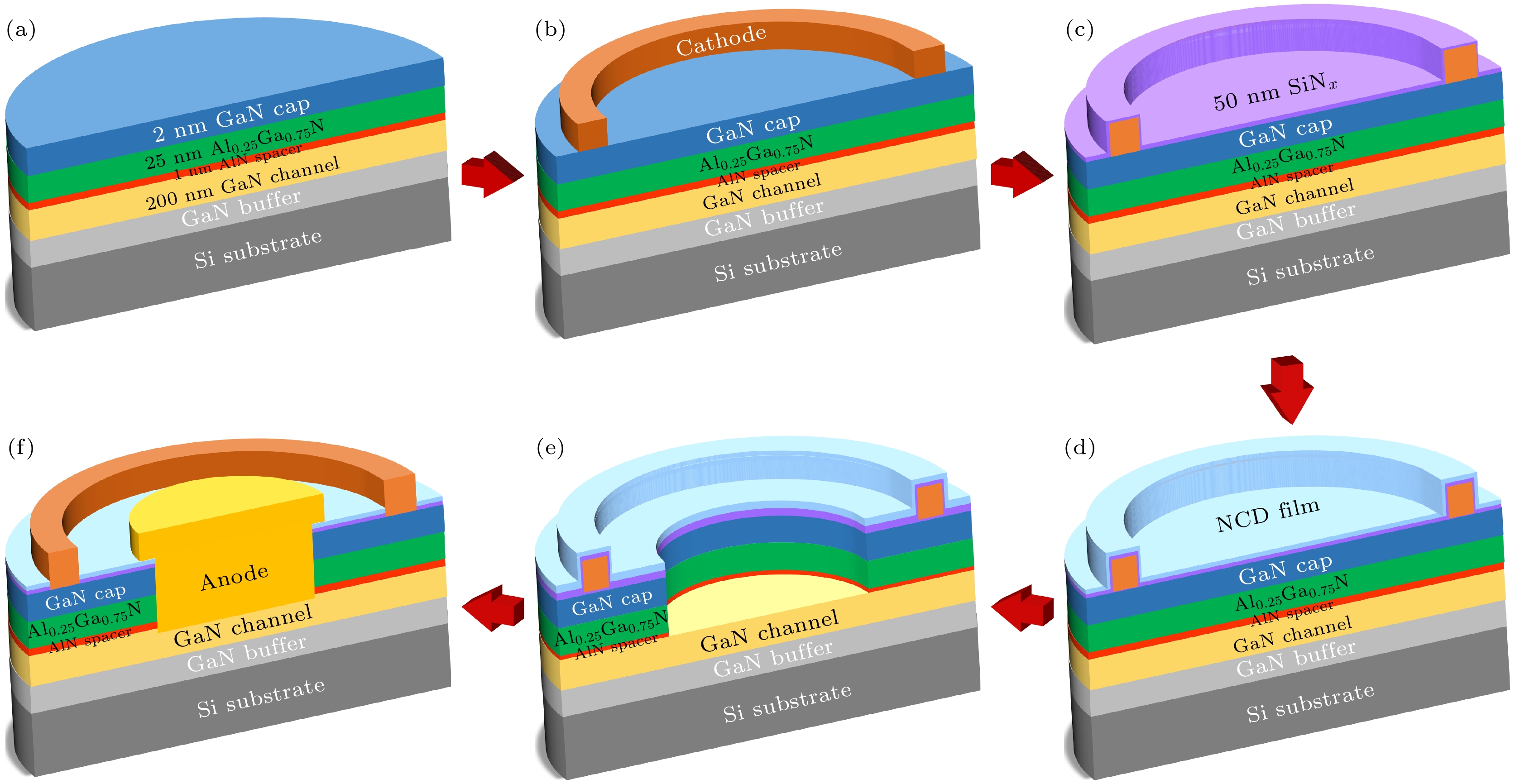
图 2 纳米晶金刚石钝化GaN基SBD主要工艺流程示意图 (a) 材料清洗与台面隔离; (b) 与欧姆阴极制作; (c) SiNx隔离层淀积; (d) 纳米晶金刚石薄膜生长; (e) 多步刻蚀暴露阳极区域; (f) 肖特基阳极制作与阴极开孔
Fig. 2. Main fabrication process flow diagram of nano crystalline diamond-passivated GaN-based SBD: (a) Sample cleaning and mesa isolation; (b) ohmic cathode formation; (c) deposition of SiNx isolation layer; (d) growth of nano crystalline diamond film; (e) multi-step etching to expose the anode region; (f) fabrication of Schottky anode and cathode opening.
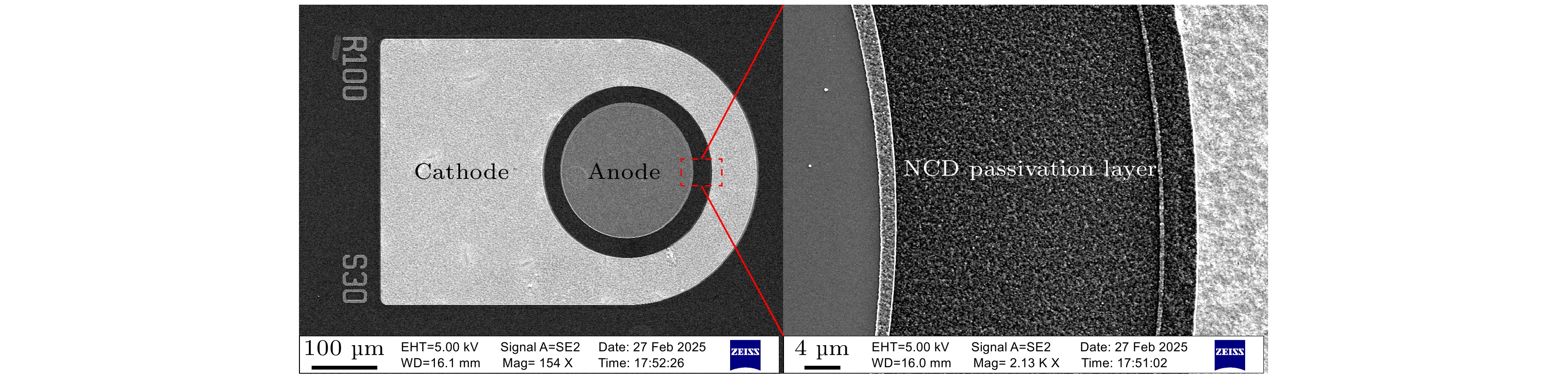
图 3 纳米晶金刚石钝化AlGaN/GaN肖特基二极管(器件A) SEM显微图像
Fig. 3. SEM micrograph of AlGaN/GaN SBD with nano crystalline diamond passivation layer (device A).
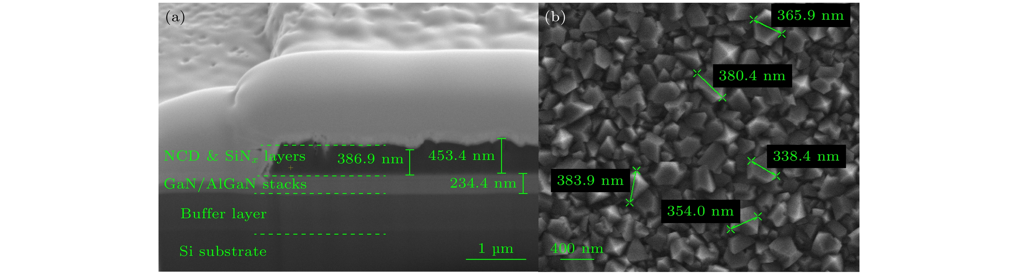
图 4 纳米晶金刚石薄膜SEM显微图像 (a) 截面; (b) 表面形貌
Fig. 4. SEM micrograph of nano crystalline diamond film: (a) Cross-section; (b) surface morphology.
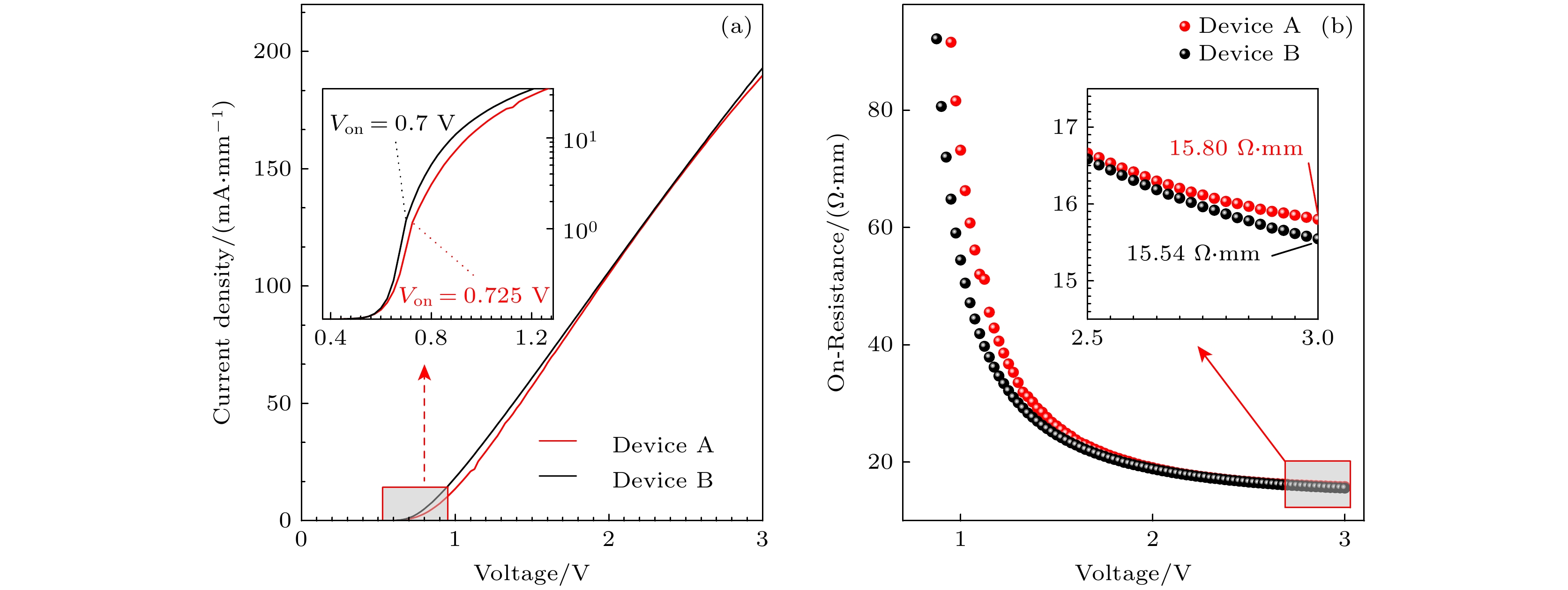
图 5 器件A和器件B静态正向特性对比 (a) 电流-电压特性; (b) 导通电阻特性
Fig. 5. Comparison of static forward characteristics between device A and device B: (a) I-V characteristics; (b) on-resistance characteristics.
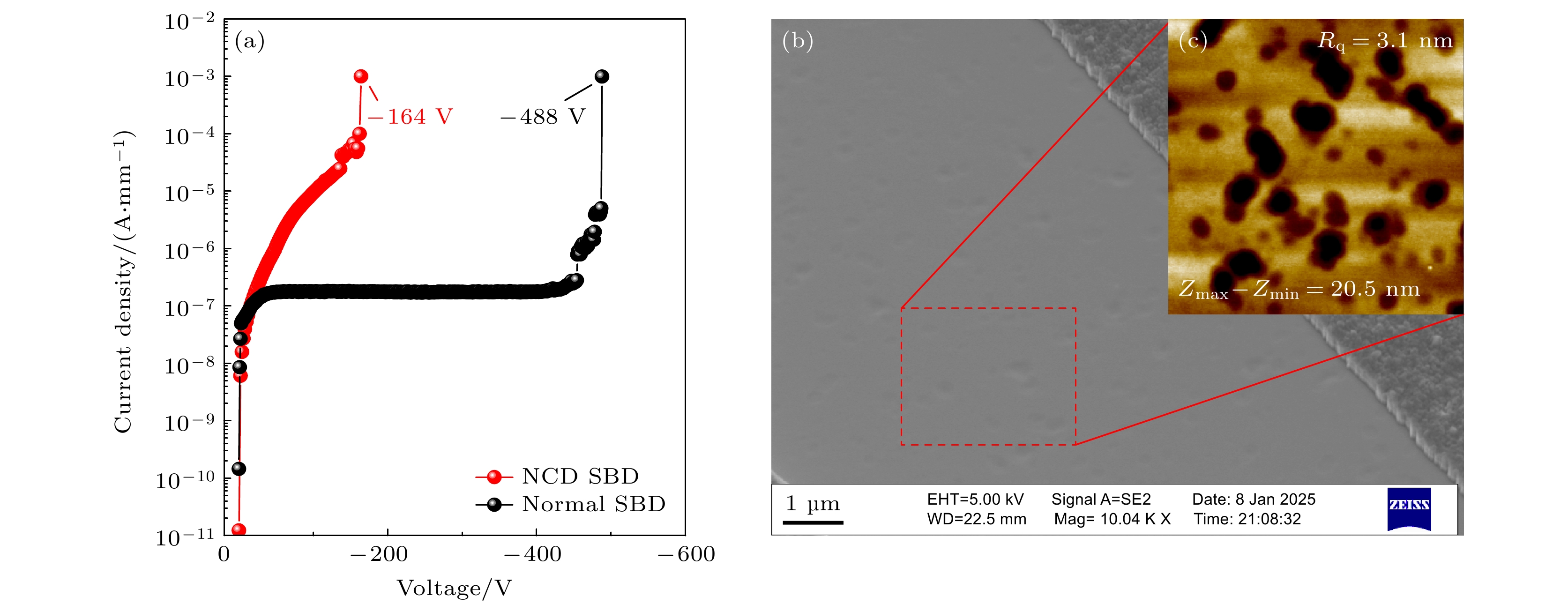
图 6 (a) NCD钝化SBD与常规器件反向特性对比; (b) 刻蚀完成后阳极区域SEM显微图像; (c) 刻蚀完成后阳极区域AFM显微图像
Fig. 6. (a) Comparison of reverse characteristics between NCD-passivated SBD and conventional device; (b) SEM micrograph of the anode region after etching; (c) AFM micrograph of the anode region after etching.
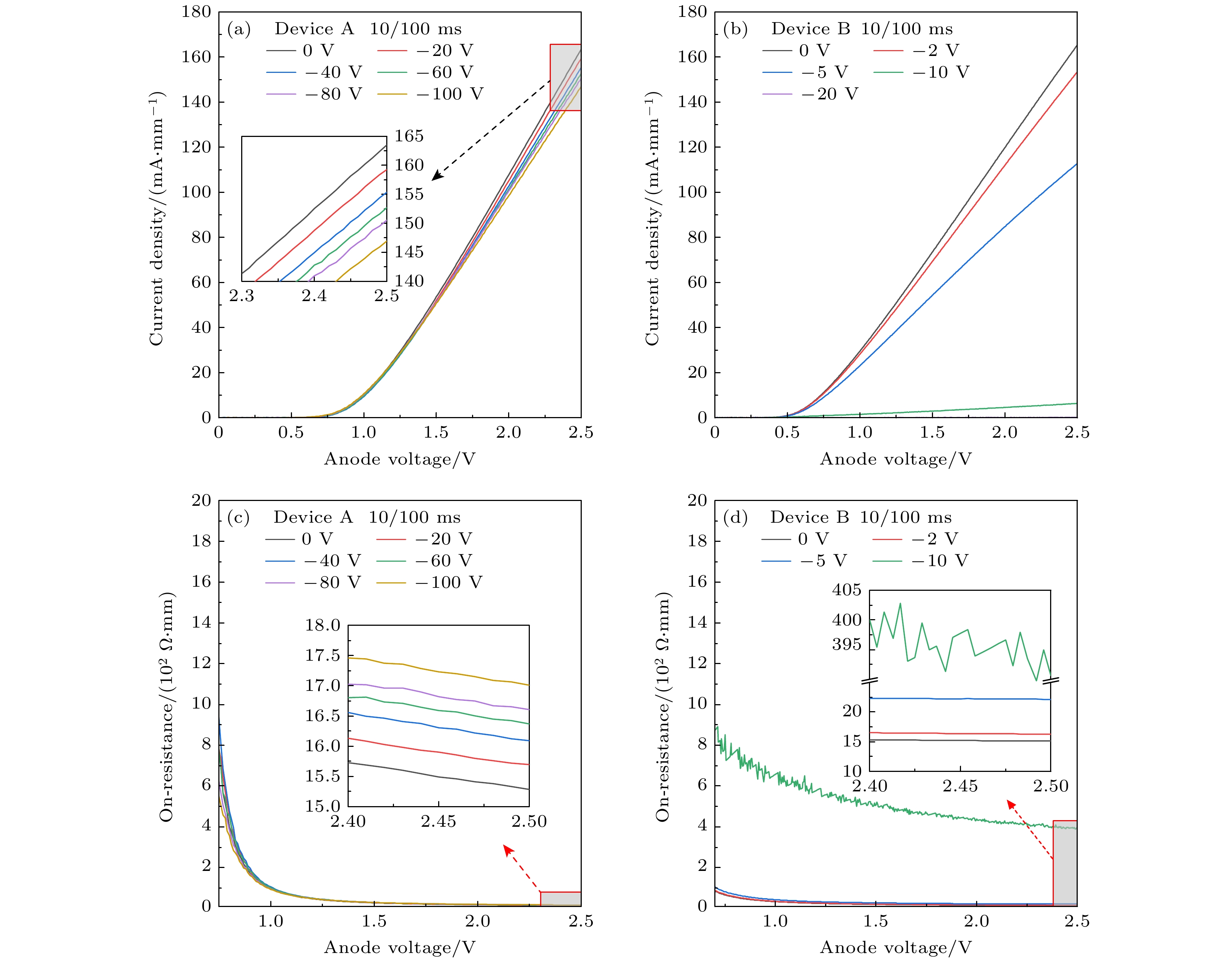
图 7 器件A和器件B的动态正向特性对比 (a) 器件A脉冲电流-电压特性; (b) 器件B脉冲电流-电压特性; (c) 器件A动态导通电阻特性; (d) 器件B动态导通电阻特性
Fig. 7. Comparison of dynamic forward characteristics between device A and B: (a) Pulsed I-V characteristics of device A; (b) pulsed I-V characteristics of device B; (c) dynamic on-resistance characteristics of device A; (d) dynamic on-resistance characteristics of device B.
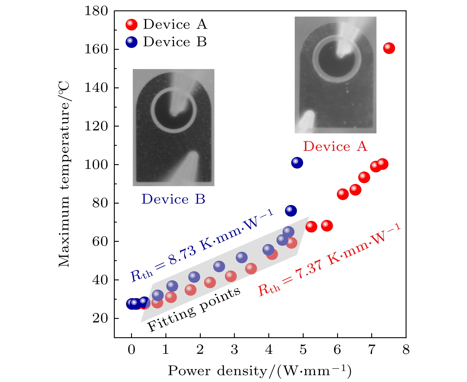
图 8 器件A, B的变功率最高结温对比
Fig. 8. Comparison of junction temperature under varying power conditions between devices A and B.
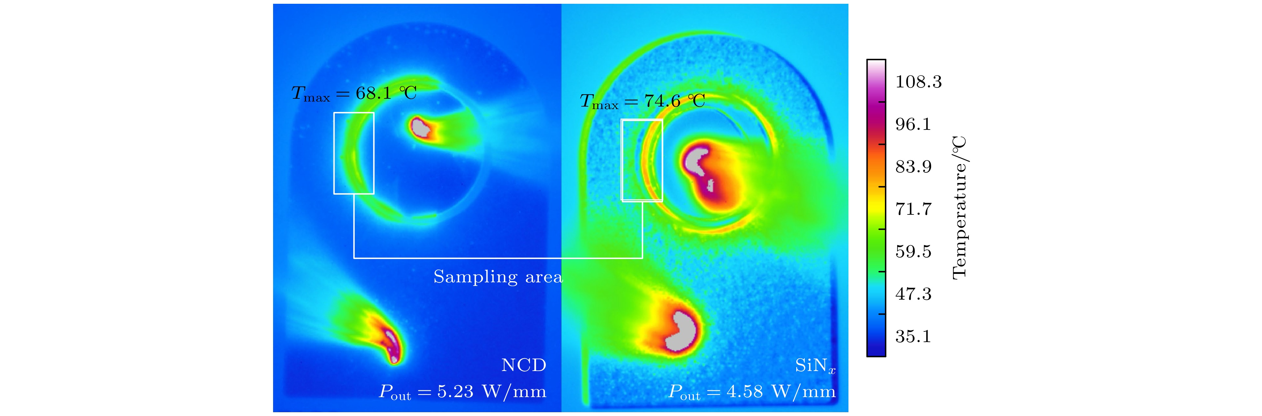
图 9 器件A, B的定功率热成像温度分布
Fig. 9. Thermal imaging temperature distribution of devices A and B under certain output power density.
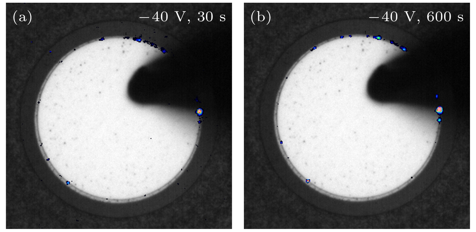
图 11 器件A反向应力微光显微镜测试结果
Fig. 11. EMMI microscopy test results of device A after reverse stress applied.
-
[1] Bader S J, Lee H, Chaudhuri R, Huang S M, Hickman A, Molnar A, Xing H L G, Jena D, Then H W, Chowdhury N, Palacios T 2020 IEEE Trans. Electron Devices 67 4010
Google Scholar
[2] Qin Y, Albano B, Spencer J, Lundh J S, Wang B, Buttay C, Tadjer M, DiMarino C, Zhang Y H 2023 J. Phys. D: Appl. Phys 56 093001
Google Scholar
[3] Minoura Y, Ohki T, Okamoto N, Sato M, Ozaki S, Yamada A, Kotani J 2022 Appl. Phys. Express 15 036501
Google Scholar
[4] Ding Y J, Li J Y, Hao Z L, Wang Q, Zhang H J, Peng Y, Chen M X 2024 IEEE Photonics Technol. Lett. 36 1005
Google Scholar
[5] Gerrer T, Pomeroy J, Yang F Y, Francis D, Carroll J, Loran B, Witkowski L, Yarborough M, Uren M J, Kuball M 2021 IEEE Trans. Electron Devices 68 1530
Google Scholar
[6] Malakoutian M, Kasperovich A, Rich D, Woo K, Perez C, Soman R, Saraswat D, Kim J K, Noshin M, Chen M, Vaziri S, Bao X Y, Shih C C, Woon W Y, Asheghi M, Goodson K E, Liao S S, Mitra S, Chowdhury S 2023 Cell Rep. Phys. Sci. 4 101686
Google Scholar
[7] Wang Y N, Hu X F, Ge L, Liu Z H, Xu M S, Peng Y, Li B, Yang Y Q, Li S Q, Xie X J, Wang X W, Xu X G, Hu X B 2023 Crystals 13 500
Google Scholar
[8] Rossi S, Alomari M, Zhang Y, Bychikhin S, Pogany D, Weaver J M R, Kohn E 2013 Diamond Relat. Mater. 40 69
Google Scholar
[9] Matsumae T, Kurashima Y, Takagi H, Shirayanagi Y, Hiza S, Nishimura K, Higurashi E 2022 Scr. Mater. 215 114725
Google Scholar
[10] Gao R H, Wang X H, Mu F W, Li X J, Wei C, Zhou W, Shi J A, Tian Y, Xing X J, Li H Y, Huang S, Jiang Q M, Wei K, Liu X Y 2024 J. Alloys Compd. 985 174075
Google Scholar
[11] Tadjer M J, Anderson T J, Ancona M G, Raad P E, Komarov P, Bai T, Gallagher J C, Koehler A D, Goorsky M S, Francis D A, Hobart K D, Kub F J 2019 IEEE Electron Device Lett. 40 881
Google Scholar
[12] 白玲, 宁静, 张进成, 王东, 王博宇, 武海迪, 赵江林, 陶然, 李忠辉 2023 人工晶体学报 52 901
Google Scholar
Bai L, Ning J, Zhang J C, Wang D, Wang B Y, Wu H D, Zhao J L, Tao R, Li Z H 2023 J. Synth. Cryst. 52 901
Google Scholar
[13] Gu Y, Zhang Y, Hua B, Ni X, Fan Q, Gu X 2021 J. Electron. Mater. 50 4239
Google Scholar
[14] 兰飞飞, 刘莎莎, 房诗舒, 王英民, 程红娟 2024 人工晶体学报 53 913
Google Scholar
Lan F F, Liu S S, Fang S S, Wang Y M, Cheng H J 2024 J. Synth. Cryst. 53 913
Google Scholar
[15] Zheng Y T, Li C M, Liu J L, Wei J J, Ye H T 2021 Funct. Diamond 1 63
Google Scholar
[16] Yang H, Ma Y, Dai Y 2021 Funct. Diamond 1 150
Google Scholar
[17] Anderson T J, Hobart K D, Tadjer M J, Koehler A D, Imhoff E A, Hite J K, Feygelson T I, Pate B B, Eddy C R, Kub F J 2016 ECS J. Solid State Sci. Technol. 6 Q3036
Google Scholar
[18] Guo H, Li Y, Yu X, Zhou J, Kong Y 2022 Micromachines (Basel) 13 1486
Google Scholar
[19] Zhou X Y, Malakoutian M, Soman R, Bian Z L, Martinez R P, Chowdhury S 2022 IEEE Trans. Electron Devices 69 6650
Google Scholar
[20] 刘庆彬, 蔚翠, 郭建超, 马孟宇, 何泽召, 周闯杰, 高学栋, 余浩, 冯志红 2023 72 098104
Google Scholar
Liu Q B, Yu C, Guo J C, Ma M Y, He Z Z, Zhou C J, Gao X D, Yu H, Feng Z H 2023 Acta Phys. Sin. 72 098104
Google Scholar
[21] Ryou J H, Choi S 2022 Nat. Electron. 5 834
Google Scholar
[22] Tadjer M J, Anderson T J, Hobart K D, Feygelson T I, Caldwell J D, Eddy C R, Kub F J, Butler J E, Pate B, Melngailis J 2012 IEEE Electron. Device Lett. 33 23
Google Scholar
[23] Meyer D J, Koehler A D, Hobart K D, Eddy C R, Feygelson T I, Anderson T J, Roussos J A, Tadjer M J, Downey B P, Katzer D S, Pate B B, Ancona M G 2014 IEEE Electron. Device Lett. 35 1013
Google Scholar
[24] Johnstone D, Doğan S, Leach J, Moon Y T, Fu Y, Hu Y, Morkoç H 2004 Appl. Phys. Lett. 85 4058
Google Scholar


 下载:
下载:


计量
- 文章访问数: 1390
- PDF下载量: 46
- 被引次数: 0
