


-
半导体与金属接触是制作纳电子和光电子器件时非常重要的问题, 接触类型对器件的功能实现和性能影响很大. 为了制备高性能多功能化器件, 就必须对界面处的势垒高度和接触类型进行调控. 采用基于密度泛函理论的第一性原理计算研究了外电场作用下graphene/InSe范德瓦耳斯异质结的电子结构. 计算结果表明异质结中的graphene和InSe保留了各自的本征电子性质, 在界面处形成了欧姆接触. 外电场可以有效调控graphene/InSe异质结中的肖特基势垒, 不但可以调控肖特基势垒的高度, 而且可以调控界面接触类型. 外电场还可以有效调控graphene和InSe界面电荷转移的数量和方向.
-
关键词:
- 肖特基势垒 /
- 电场 /
- graphene/InSe范德瓦耳斯异质结
The contacts between semiconductor and metal are vital in the fabrication of nano electronic and optoelectronic devices. The contact type has a great influence on the function realization and performance of the device. In order to prepare multifunctional devices with high performance, it is necessary to modulate the barrier height and contact type at the interface. First-principles calculations based on the density functional theory (DFT) are implemented in the VASP package. The generalized gradient approximation of Perdew, Burke, and Ernzerhof (GGA-PBE) with van der Waals (vdW) correction proposed by Grimme (DFT-D3) is chosen due to its good description of long-range vdW interactions. It is demonstrated that weak vdW interactions dominate between graphene and InSe with their intrinsic electronic properties preserved. We find that the n-type ohmic contact is formed at the graphene/InSe interface with the Fermi level through the conduction band of InSe (ΦBn < 0). The Fermi level of graphene/InSe heterostructure moves down to below the Dirac point of graphene layer, which results in p-type (hole) doping in graphene. Moreover, the external electric field is effective to tune the Schottky barrier, which can control not only the Schottky barrier height but also the type of contact. With the negative external electric field varying from 0 to –1 V/nm, the conduction band minimum of InSe below the Fermi level declines gradually but the n-type ohmic contact is still preserved. Nevertheless, with the positive external electric field varying from 0 to 0.8 V/nm, the conduction band minimum of InSe shifts upward and across the Fermi level, the conduction band minimum of InSe is closer to the Fermi level than the valence band maximum, which indicates that the n-type Schottky contact is formed. The Fermi level moves from the the conduction band minimum to the valence band maximum of InSe when the positive external electric field increases from 0.8 V/nm to 2 V/nm. The n-type Schottky barrier height exceeds the p-type Schottky barrier height gradually, which demonstrates that the positive external electric field transforms the n-type Schottky contact into the p-type Schottky contact at the graphene/InSe interface. When the positive external electric field exceeds 2 V/nm, the valence band of InSe moves upward and cross the Fermi level (ΦBp < 0), the ohmic contact is obtained again. Meanwhile, p-type (hole) doping in graphene is enhanced under negative external electric field and a large positive external electric field is required to achieve n-type (electron) doping in graphene. The external electric field can control not only the amount of charge transfer but also the direction of charge transfer at the graphene/InSe interface.[1] Novoselov K S, Geim A K, Morozov S V, et al. 2004 Science 306 666
 Google Scholar
[2] Novoselov K S, Geim A K, Morozov S V, et al. 2005 Nature 438 197
Google Scholar
[3] Neto A C, Guinea F, Peres N M, Novoselov K S, Geim A K 2009 Rev. Mod. Phys. 81 109
Google Scholar
[4] Tang Q, Zhou Z 2013 Prog. Mater. Sci. 58 1244
Google Scholar
[5] Schwierz F 2010 Nat. Nanotechnol. 5 487
Google Scholar
[6] Balog R, Jørgensen B, Nilsson L, et al. 2010 Nat. Mater. 9 315
Google Scholar
[7] Han M Y, Ozyilmaz B, Zhang Y, Kim P 2007 Phys. Rev. Lett. 98 206805
Google Scholar
[8] Huang L, Huo N J, Li Y, Chen H, Yang J H, Wei Z M, Li J B, Li S S 2015 J. Phys. Chem. Lett. 6 2483
Google Scholar
[9] Kang J, Sahin H, Peeters F M 2015 J. Phys. Chem. C 119 9580
Google Scholar
[10] Yu J H, Lee H R, Hong S S, Kong D S, Lee H W, Wang H T, Xiong F, Wang S, Cui Y 2015 Nano Lett. 15 1031
Google Scholar
[11] Xiang Q J, Yu J G, Jaroniec M 2011 J. Phys. Chem. C 115 7355
Google Scholar
[12] Li X H, Chen J S, Wang X, Sun J, Antonietti M 2011 J. Am. Chem. Soc. 133 8074
Google Scholar
[13] Du A, Sanvito S, Li Z, et al. 2012 J. Am. Chem. Soc. 134 4393
Google Scholar
[14] Dean C R, Young A F, Meric I, et al. 2010 Nat. Nanotechnol. 5 722
Google Scholar
[15] Xue J, Sanchez-Yamagishi J, Bulmash D, et al. 2011 Nat. Mater. 10 282
Google Scholar
[16] Sławin′ska J, Zasada I, Klusek Z 2010 Phys. Rev. B 81 155433
Google Scholar
[17] Lin X, Xu Y, Hakro A A, Hasan T, Hao R, Zhang B, Chen H 2013 J. Mater. Chem. C 1 1618
Google Scholar
[18] Ma Y, Dai Y, Guo M, Niu C, Huang B 2011 Nanoscale 3 3883
Google Scholar
[19] Li X D, Yu S, Wu S Q, Wen Y H, Zhou S, Zhu Z Z 2013 J. Phys. Chem. C 117 15347
Google Scholar
[20] Britnell L, Ribeiro R M, Eckmann A, et al. 2013 Science 340 1311
Google Scholar
[21] Tian H, Tan Z, Wu C, et al. 2014 Sci. Rep. 4 5951
[22] Tung R 2014 Appl. Phys. Rev. 1 011304
Google Scholar
[23] Mudd G, Patane A, Kudrynskyi Z, et al. 2014 Appl. Phys. Lett. 105 221909
Google Scholar
[24] Wu M, Shi J, Zhang M, Ding Y, Wang H, Cen Y, Lu J 2018 Nanoscale 10 11441
Google Scholar
[25] Ho P H, Chang Y R, Chu Y C, Li M K, Tsai C A, Wang W H, Ho C H, Chen C W, Chiu P W 2017 ACS Nano 11 7362
Google Scholar
[26] Tamalampudi S, Lu Y, Kumar U, Sankar R, Liao C, Moorthy B, Cheng C, Chou F, Chen Y 2014 Nano Lett. 14 2800
Google Scholar
[27] Lei S, Ge L, Najmaei S, et al. 2014 ACS Nano 8 1263
Google Scholar
[28] Sun C, Xiang H, Xu B, Xia Y, Yin J, Liu Z 2016 Appl. Phys. Express 9 035203
Google Scholar
[29] Bandurin D A, Tyurnina A V, Yu G L, et al. 2017 Nat. Nanotechnol. 12 223
Google Scholar
[30] Feng W, Zheng W, Cao W, Hu P 2014 Adv. Mater. 26 6587
Google Scholar
[31] Padilha J E, Miwa R H, Silva A J R, Fazzio A 2017 Phys. Rev. B 95 195143
Google Scholar
[32] Yan F, Zhao L, Patane A, Hu P, Wei X, Luo W, Zhang D, Lv Q, Feng Q, Shen C, Chang K, Eaves L, Wang K 2017 Nanotechnology 28 27LT01
Google Scholar
[33] Mudd G W, Svatek S A, Hague L, et al. 2015 Adv. Mater. 27 3760
Google Scholar
[34] Blöchl P E 1994 Phys. Rev. B 50 17953
Google Scholar
[35] Kresse G, Furthmüller J 1996 Phys. Rev. B 54 11169
Google Scholar
[36] Perdew J P, Burke K, Ernzerhof M 1996 Phys. Rev. Lett. 77 3865
Google Scholar
[37] Grimme S 2006 J. Comput. Chem. 27 1787
Google Scholar
[38] Singh S, Espejo C, Romero A 2018 Phys. Rev. B 98 155309
Google Scholar
[39] Woessner A, Lundeberg M B, Gao Y, et al. 2015 Nat. Mater. 14 421
Google Scholar
[40] Zhuang H L, Hennig R G 2013 Chem. Mater. 25 3232
Google Scholar
[41] Sun M, Chou J P, Yu J, Tang W 2017 J. Mater. Chem. C 5 10383
Google Scholar
-

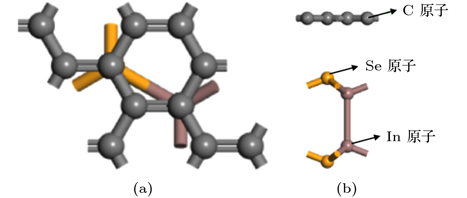
图 2 (a) Graphene/InSe异质结的顶视图; (b) graphene/InSe异质结的顶视图; 灰色、橙色和棕色小球分别表示碳原子、硒原子和铟原子
Fig. 2. Top view (a) and side view (b) of the graphene/InSe heterostructures. The gray, orange and brown balls are for C, Se and In atoms, respectively.
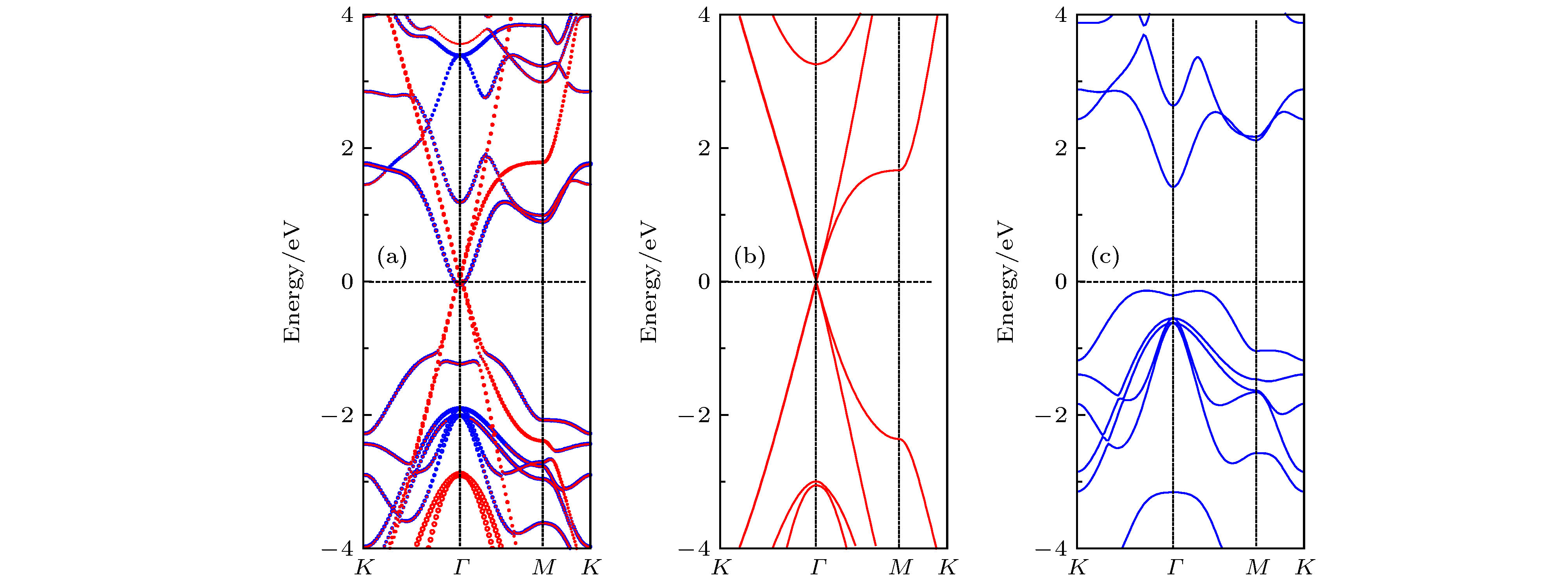
图 3 (a) Graphene/InSe异质结的投影能带结构图, 红色线条表示graphene的能带, 蓝色线条表示InSe的能带; (b) graphene的能带结构图; (c)单层InSe的能带结构图; 费米能级设为零点
Fig. 3. (a) Projected band structure of the graphene/InSe heterostructure, where the red and blue lines represent for the energy band of graphene and InSe, respectively; (b) the band structure of graphene; (c) the band structure of monolayer InSe. The Fermi level is set to zero.
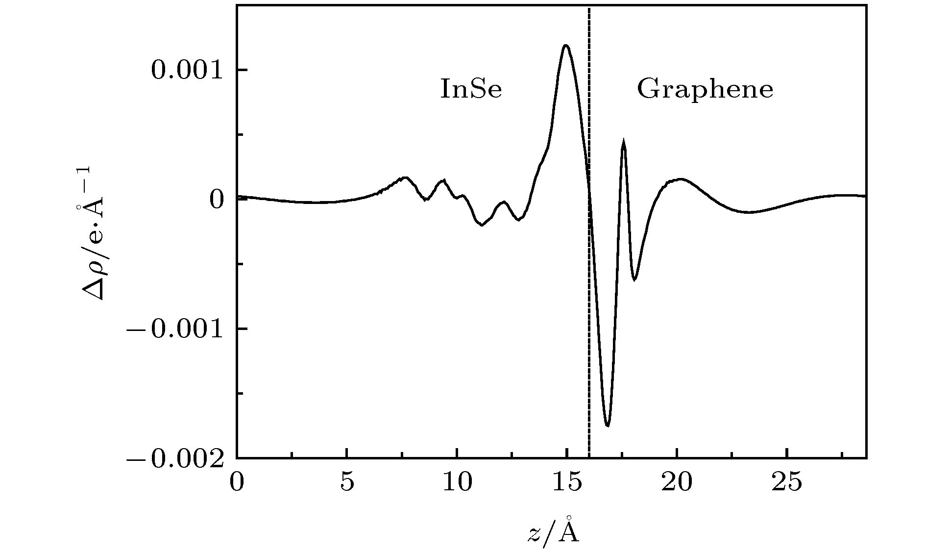
图 4 Graphene/InSe异质结的平面平均差分电荷密度图, 图中的竖直黑色虚线表示graphene层和InSe层的分界线
Fig. 4. Plane-averaged charge density difference of the graphene/InSe heterostructure. The black vertical dashed line denotes the intermediate position of graphene and InSe.
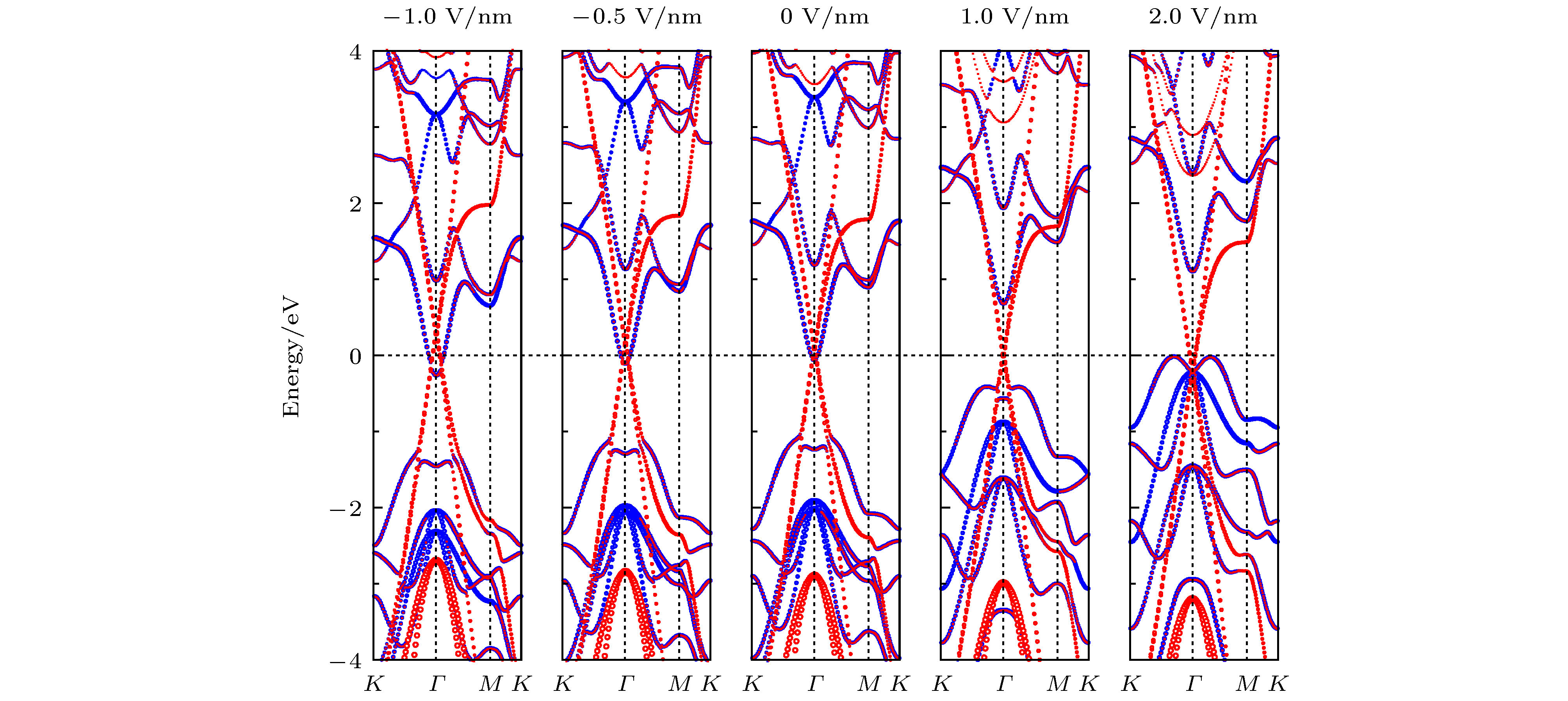
图 5 施加不同外电场时graphene/InSe异质结的投影能带图, 图中蓝色线条表示InSe的能带, 红色线条表示graphene的能带, 费米能级设为零点
Fig. 5. Projected band structures of graphene/InSe heterostructures under different external electric fields. The red and blue lines represent for the energy band of graphene and InSe, respectively. The Fermi level is set to zero.
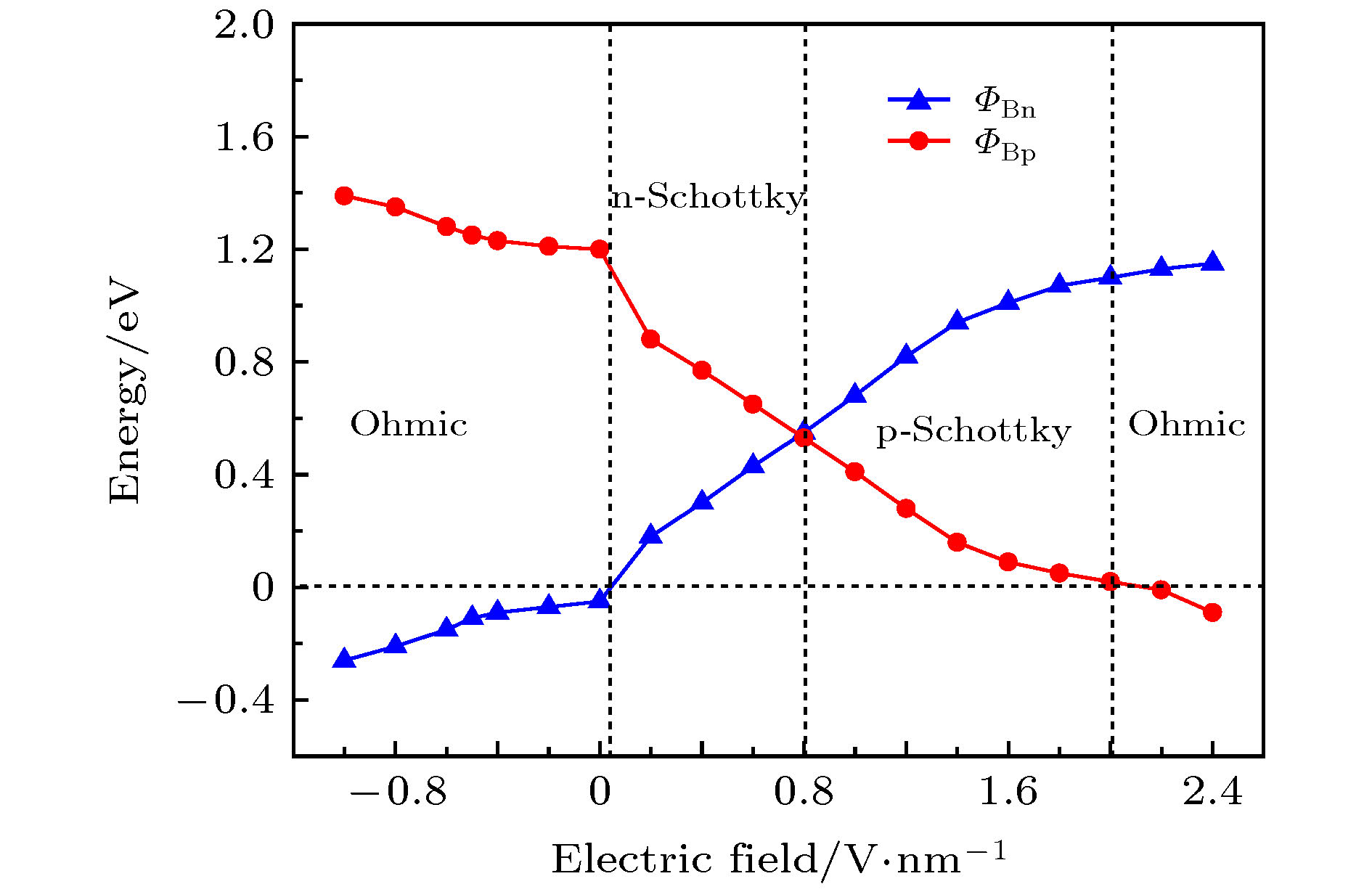
图 6 Graphene/InSe异质结的肖特基势垒随外电场的变化
Fig. 6. Evolution of Schottky barriers of the graphene/InSe heterostructurer as a function of external electric field.
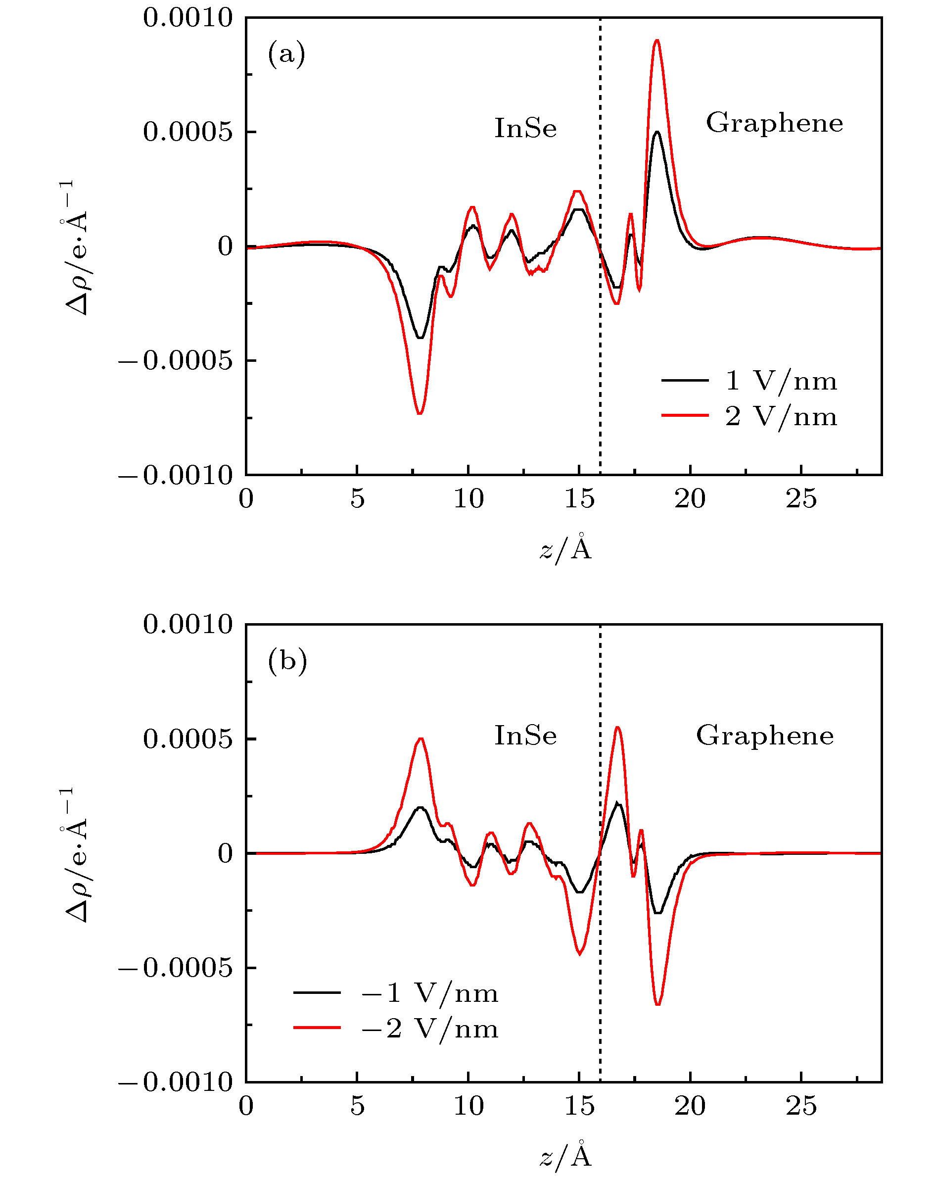
图 7 (a) 施加正外电场时graphene/InSe异质结的平面平均差分电荷密度图; (b) 施加负外电场时graphene/InSe异质结的平面平均差分电荷密度图; 图中的竖直黑色虚线表示graphene层和InSe层的分界线
Fig. 7. (a) Plane-averaged charge density difference of the graphene/InSe heterostructure under positive external electric fields; (b) the plane-averaged charge density difference of the graphene/InSe heterostructure under negative external electric fields. The black vertical dashed line denotes the intermediate position of graphene and InSe.
-
[1] Novoselov K S, Geim A K, Morozov S V, et al. 2004 Science 306 666
Google Scholar
[2] Novoselov K S, Geim A K, Morozov S V, et al. 2005 Nature 438 197
Google Scholar
[3] Neto A C, Guinea F, Peres N M, Novoselov K S, Geim A K 2009 Rev. Mod. Phys. 81 109
Google Scholar
[4] Tang Q, Zhou Z 2013 Prog. Mater. Sci. 58 1244
Google Scholar
[5] Schwierz F 2010 Nat. Nanotechnol. 5 487
Google Scholar
[6] Balog R, Jørgensen B, Nilsson L, et al. 2010 Nat. Mater. 9 315
Google Scholar
[7] Han M Y, Ozyilmaz B, Zhang Y, Kim P 2007 Phys. Rev. Lett. 98 206805
Google Scholar
[8] Huang L, Huo N J, Li Y, Chen H, Yang J H, Wei Z M, Li J B, Li S S 2015 J. Phys. Chem. Lett. 6 2483
Google Scholar
[9] Kang J, Sahin H, Peeters F M 2015 J. Phys. Chem. C 119 9580
Google Scholar
[10] Yu J H, Lee H R, Hong S S, Kong D S, Lee H W, Wang H T, Xiong F, Wang S, Cui Y 2015 Nano Lett. 15 1031
Google Scholar
[11] Xiang Q J, Yu J G, Jaroniec M 2011 J. Phys. Chem. C 115 7355
Google Scholar
[12] Li X H, Chen J S, Wang X, Sun J, Antonietti M 2011 J. Am. Chem. Soc. 133 8074
Google Scholar
[13] Du A, Sanvito S, Li Z, et al. 2012 J. Am. Chem. Soc. 134 4393
Google Scholar
[14] Dean C R, Young A F, Meric I, et al. 2010 Nat. Nanotechnol. 5 722
Google Scholar
[15] Xue J, Sanchez-Yamagishi J, Bulmash D, et al. 2011 Nat. Mater. 10 282
Google Scholar
[16] Sławin′ska J, Zasada I, Klusek Z 2010 Phys. Rev. B 81 155433
Google Scholar
[17] Lin X, Xu Y, Hakro A A, Hasan T, Hao R, Zhang B, Chen H 2013 J. Mater. Chem. C 1 1618
Google Scholar
[18] Ma Y, Dai Y, Guo M, Niu C, Huang B 2011 Nanoscale 3 3883
Google Scholar
[19] Li X D, Yu S, Wu S Q, Wen Y H, Zhou S, Zhu Z Z 2013 J. Phys. Chem. C 117 15347
Google Scholar
[20] Britnell L, Ribeiro R M, Eckmann A, et al. 2013 Science 340 1311
Google Scholar
[21] Tian H, Tan Z, Wu C, et al. 2014 Sci. Rep. 4 5951
[22] Tung R 2014 Appl. Phys. Rev. 1 011304
Google Scholar
[23] Mudd G, Patane A, Kudrynskyi Z, et al. 2014 Appl. Phys. Lett. 105 221909
Google Scholar
[24] Wu M, Shi J, Zhang M, Ding Y, Wang H, Cen Y, Lu J 2018 Nanoscale 10 11441
Google Scholar
[25] Ho P H, Chang Y R, Chu Y C, Li M K, Tsai C A, Wang W H, Ho C H, Chen C W, Chiu P W 2017 ACS Nano 11 7362
Google Scholar
[26] Tamalampudi S, Lu Y, Kumar U, Sankar R, Liao C, Moorthy B, Cheng C, Chou F, Chen Y 2014 Nano Lett. 14 2800
Google Scholar
[27] Lei S, Ge L, Najmaei S, et al. 2014 ACS Nano 8 1263
Google Scholar
[28] Sun C, Xiang H, Xu B, Xia Y, Yin J, Liu Z 2016 Appl. Phys. Express 9 035203
Google Scholar
[29] Bandurin D A, Tyurnina A V, Yu G L, et al. 2017 Nat. Nanotechnol. 12 223
Google Scholar
[30] Feng W, Zheng W, Cao W, Hu P 2014 Adv. Mater. 26 6587
Google Scholar
[31] Padilha J E, Miwa R H, Silva A J R, Fazzio A 2017 Phys. Rev. B 95 195143
Google Scholar
[32] Yan F, Zhao L, Patane A, Hu P, Wei X, Luo W, Zhang D, Lv Q, Feng Q, Shen C, Chang K, Eaves L, Wang K 2017 Nanotechnology 28 27LT01
Google Scholar
[33] Mudd G W, Svatek S A, Hague L, et al. 2015 Adv. Mater. 27 3760
Google Scholar
[34] Blöchl P E 1994 Phys. Rev. B 50 17953
Google Scholar
[35] Kresse G, Furthmüller J 1996 Phys. Rev. B 54 11169
Google Scholar
[36] Perdew J P, Burke K, Ernzerhof M 1996 Phys. Rev. Lett. 77 3865
Google Scholar
[37] Grimme S 2006 J. Comput. Chem. 27 1787
Google Scholar
[38] Singh S, Espejo C, Romero A 2018 Phys. Rev. B 98 155309
Google Scholar
[39] Woessner A, Lundeberg M B, Gao Y, et al. 2015 Nat. Mater. 14 421
Google Scholar
[40] Zhuang H L, Hennig R G 2013 Chem. Mater. 25 3232
Google Scholar
[41] Sun M, Chou J P, Yu J, Tang W 2017 J. Mater. Chem. C 5 10383
Google Scholar


 下载:
下载:


计量
- 文章访问数: 15438
- PDF下载量: 417
- 被引次数: 0
