


-
Indium oxide (In2O3) thin films and thin-film transistors (TFTs) based on the solution process are prepared by pulsed UV-assisted thermal annealing at a low temperature (200 ℃) for 5 min. The effects of pulsed UV-assisted thermal annealing on the surface morphology, chemical structure, and electrical properties of the In2O3 thin films are investigated, and they are compared with those of conventional thermal annealing (300 ℃, 30 min). The experimental results show that the pulsed UV-assisted thermal annealing method can improve the quality of In2O3 thin film and the performance of TFT in a short period. The results of atomic force microscopy and field emission scanning electron microscopy show that the surface of the In2O3 film is denser and flatter than that of the conventional thermally annealed film, and X-ray photoelectron spectroscopy tests show that the pulsed UV-assisted thermal annealing process generates oxygen vacancies, which increases the carrier concentration and improves the electrical conductivity of the In2O3 film. In addition, the effect of pulsed UV-assisted thermal annealing on the electrical characteristics of In2O3 TFTs is investigated in a comparative way. The results show that the electrical characteristics of the device are significantly improved: the subthreshold swing decreases to 0.12 mV/dec, the threshold voltage is 7.4 V, the current switching ratio is as high as 1.29×10⁷, and the field effect mobility is enhanced to 1.27 cm2·V–1·s–1. Therefore, pulsed UV-assisted thermal annealing is a simple and fast annealing method, which can rapidly improve the performances of In2O3 thin film and TFTs, even under low-temperature conditions.
-
Keywords:
- pulsed UV-assisted thermal annealing /
- indium oxide /
- solution process /
- thin film transistor
[1] He Y L, Wang X Y, Gao Y, Hou Y H, Wan Q 2018 J. Semicond. 39 011005
 Google Scholar
[2] Zhou Y, Roy V A L, Xu Z X, Kwong H Y, Wang H B, Lee C S 2011 Appl. Phys. Lett. 98 092904
Google Scholar
[3] Liang K, Wang Y, Shao S S, Luo M M, Pecunia V, Shao L, Zhao J W, Chen Z, Mo L X, Cui Z 2019 J. Mater. Chem. C 7 6169
Google Scholar
[4] Kim S J, Yoon S H, Kim H J 2014 J. Appl. Phys. 53 02BA02
Google Scholar
[5] Choi C H, Han S Y, Su Y W, Fang Z, Lin L Y, Cheng C C, Chang C H 2015 J. Mater. Chem. C 3 854
Google Scholar
[6] Kim M G, Kanatzidis M G, Facchetti A, Marks T J 2011 Nat. Mater. 10 382
Google Scholar
[7] Hwang Y H, Seo J S, Yun J M, Park H J, Yang S H, Park S H K, Bae B S 2013 NPG Asia Mater. 5 e45
Google Scholar
[8] Lee H J, Jyothi C, Baang S K , Kwon J H, Bae J H 2016 J. Korean. Phys. Soc. 69 1688
Google Scholar
[9] Zhang X, Lee H J, Kwon J H, Kim E J, Park J H 2017 Materials 10 880
Google Scholar
[10] Park J H, Park W, Na J H, Lee J U, Eun J S, Feng J H, Kim D K, Bae J H 2023 Nanomaterials 13 2568
Google Scholar
[11] 谢应涛, 蔡坤林, 陈鹏龙, 刘愈, 王东平 2022 中国激光 49 0703001
Google Scholar
Xie Y T, Cai K L, Chen P L, Liu Y, Wang D P 2022 Chin. J. Lasers 49 0703001
Google Scholar
[12] Kim W G, Tak Y J, Ahn B D, Jung T S, Chung K B, Kim H J 2016 Sci. Rep. 6 23039
Google Scholar
[13] Rahman M K, Lu Z, Kwon K S 2018 AIP Adv. 8 095008
Google Scholar
[14] Lee H W, Choi H S, Cho W J 2019 J. Nanosci. Nanotechno. 19 6164
Google Scholar
[15] Huang H Y, Wang S J, Wu C H, Lu C Y 2014 Electron. Mater. Lett. 10 899
Google Scholar
[16] Kim D W, Park J H, Hwang J U, Kim H D, Ryu J H, Lee K B, Baek K H, Do L M, Choi J S 2015 Electron. Mater. Lett. 11 82
Google Scholar
[17] Park S C, Kim D W, Shin H J, Lee D K, Zhang X, Park J H, Choi J S 2016 J. Inf. Disp. 17 179
Google Scholar
[18] Huet K, Aubin J, Raynal P E, Curvers B, Verstraete A, Lespinasse B, Mazzamuto F, Sciuto A, Lombardo S F, Magna A L, Acosta-Alba P, Dagault L, Licitra C, Hartmann J M, Kerdilès S 2020 Appl. Surf. Sci. 505 144470
Google Scholar
[19] Lee H J, Zhang X, Kim J W, Kim E J, Park J H 2018 Materials 11 2103
Google Scholar
[20] Azianty S, Saadah A R, Boon T G 2018 Mater. Today 5 S186
Google Scholar
[21] Xing R Q, Xu L, Song J, Zhou C Y, Li Q L, Liu D L, Song H W 2015 Sci. Rep. 5 10717
Google Scholar
[22] Tetzner K, Isakov I, Regoutz A, Payne D J, Anthopoulos T D 2017 J. Mater. Chem. C 5 59
Google Scholar
[23] Shinde D, Ahn D Y, Jadhav V, Lee D Y, Shrestha N K, Lee J K, Lee H, Mane R S, Han S H 2014 J. Mater. Chem. A 2 5490
Google Scholar
[24] Lin Y H, Liu Y S, Lin Y C, Wei Y S, Liao K S, Lee K R, Lai J Y, Chen H M, Jean Y C, Liu C Y 2013 J. Appl. Phys. 113 033706
Google Scholar
[25] Ide K, Nomura K, Hosono H, Kamiya T 2019 Phys. Status Solidi A 216 1800372
Google Scholar
[26] Biswas P, Ainabayev A, Zhussupbekova A, Jose F, O’Connor R, Kaisha A, Walls B, Shvets I V 2020 Sci. Rep. 10 7463
Google Scholar
[27] Tsay C Y, Liang S C 2017 Mat. Sci. Semicon. Proc. 71 441
Google Scholar
-
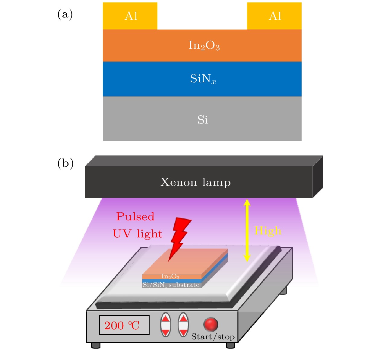
图 1 (a) In2O3 TFT的结构示意图; (b) 脉冲紫外线辅助热退火工艺的原理示意图
Figure 1. Schematic diagram of (a) structure of the prepared In2O3 TFT and (b) principle of the pulsed UV-assisted T.A.
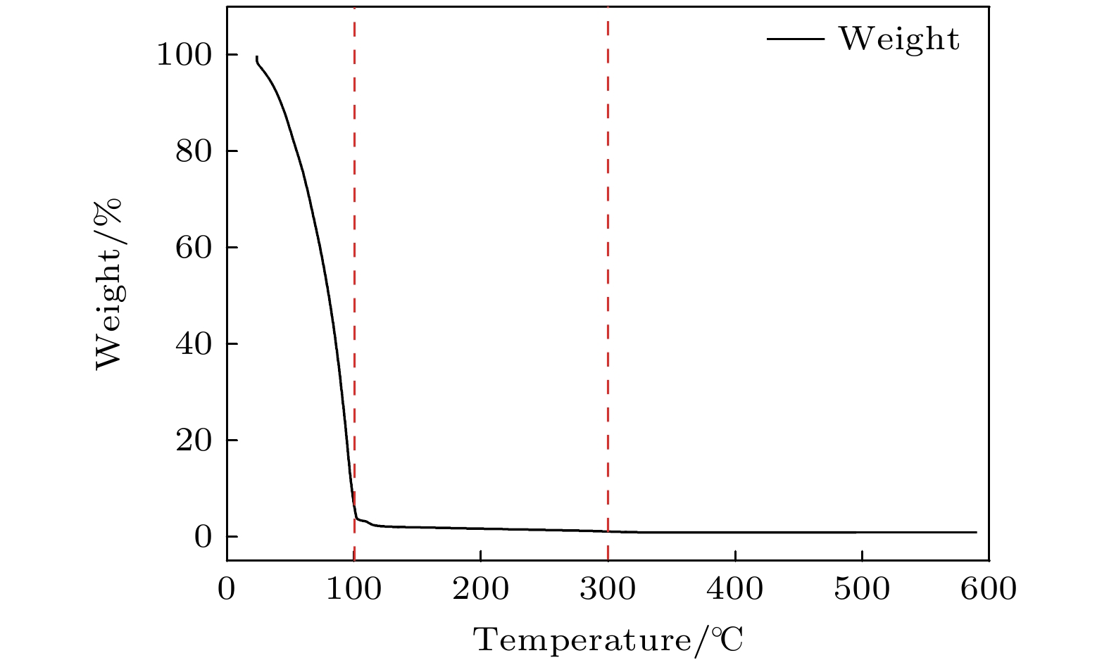
图 2 In2O3前驱体溶液的TGA曲线
Figure 2. TGA of In2O3 precursor solution.
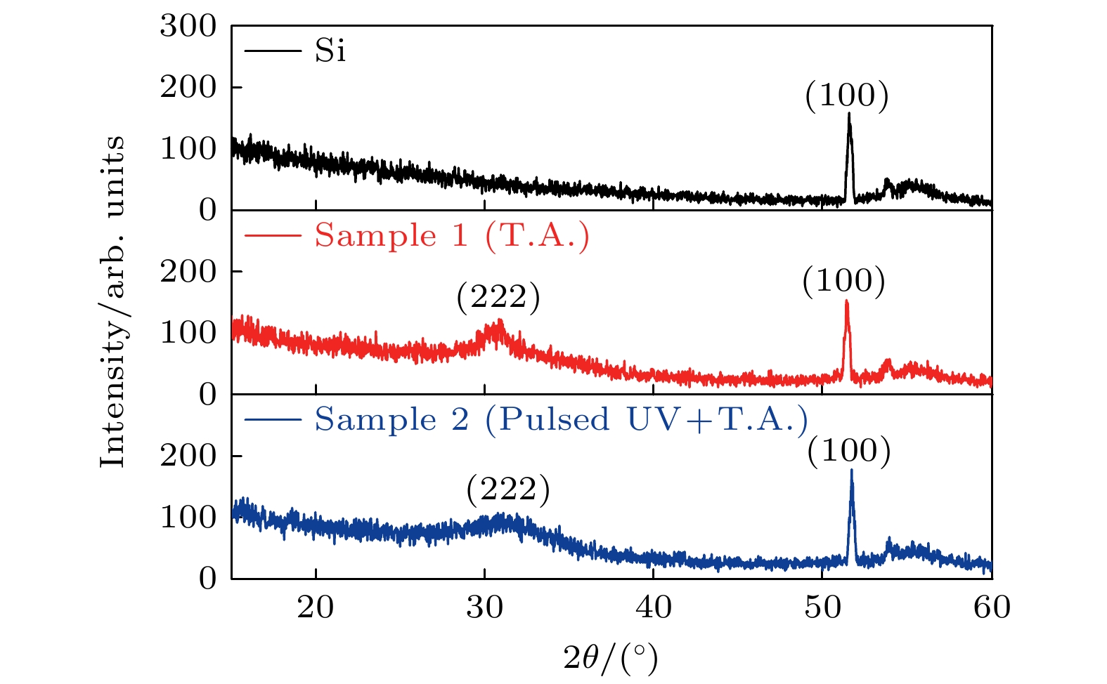
图 3 硅板、样品1 (传统热退火方式)和样品2 (脉冲紫外线辅助热退火方式)的XRD图谱
Figure 3. XRD patterns of Si substrate, Sample 1 (T.A.) and Sample 2 (pulsed UV+T.A.).
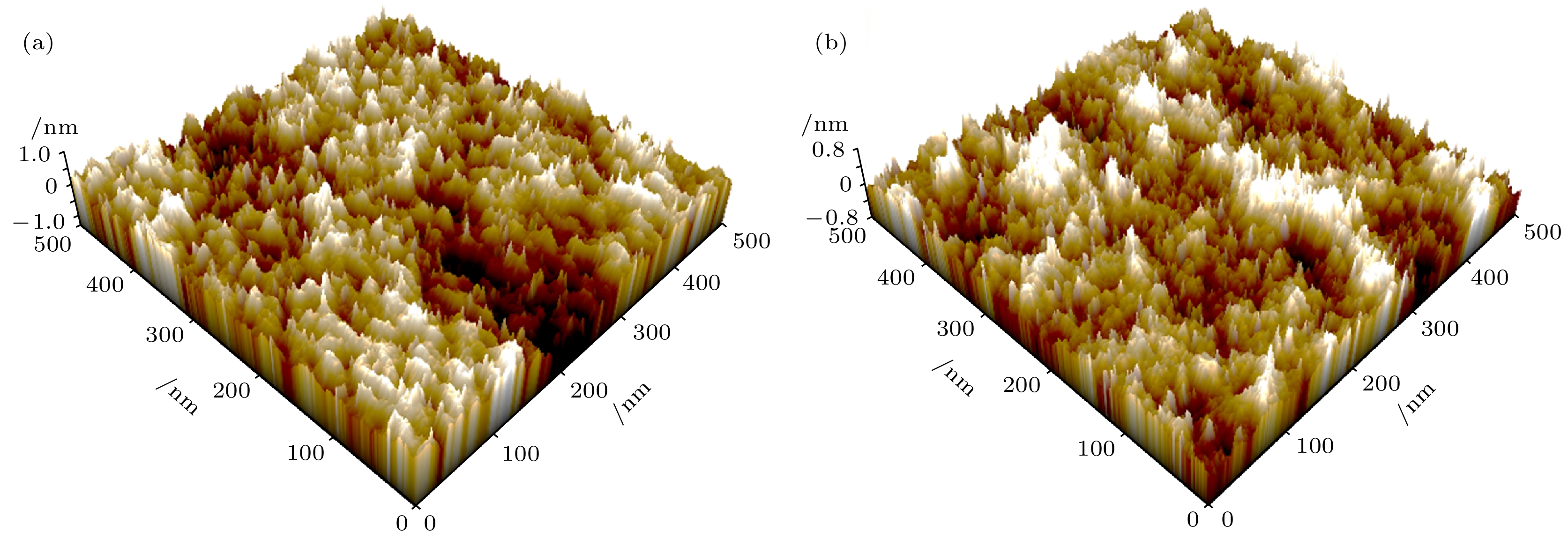
图 4 In2O3薄膜的AFM图像 (a) 样品1 (传统热退火方式); (b) 样品2 (脉冲紫外线辅助热退火方式)
Figure 4. AFM images of In2O3 thin films: (a) Sample 1 (T.A.); (b) Sample 2 (pulsed UV+T.A.).
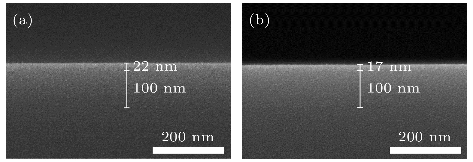
图 5 In2O3薄膜的FESEM图像 (a) 样品1 (传统热退火方式); (b) 样品2 (脉冲紫外线辅助热退火方式)
Figure 5. FESEM images of In2O3 thin films: (a) Sample 1 (T.A.); (b) Sample 2 (pulsed UV+T.A.).
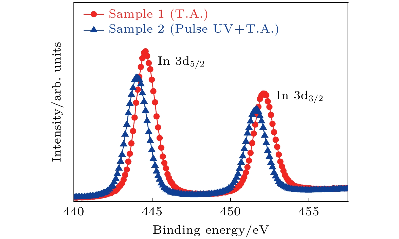
图 6 样品1 (传统热退火方式)和样品2 (脉冲紫外线辅助热退火方式)的In 3d XPS图谱
Figure 6. In 3d XPS spectra of Sample 1 (T.A.) and Sample 2 (pulsed UV+T.A.).
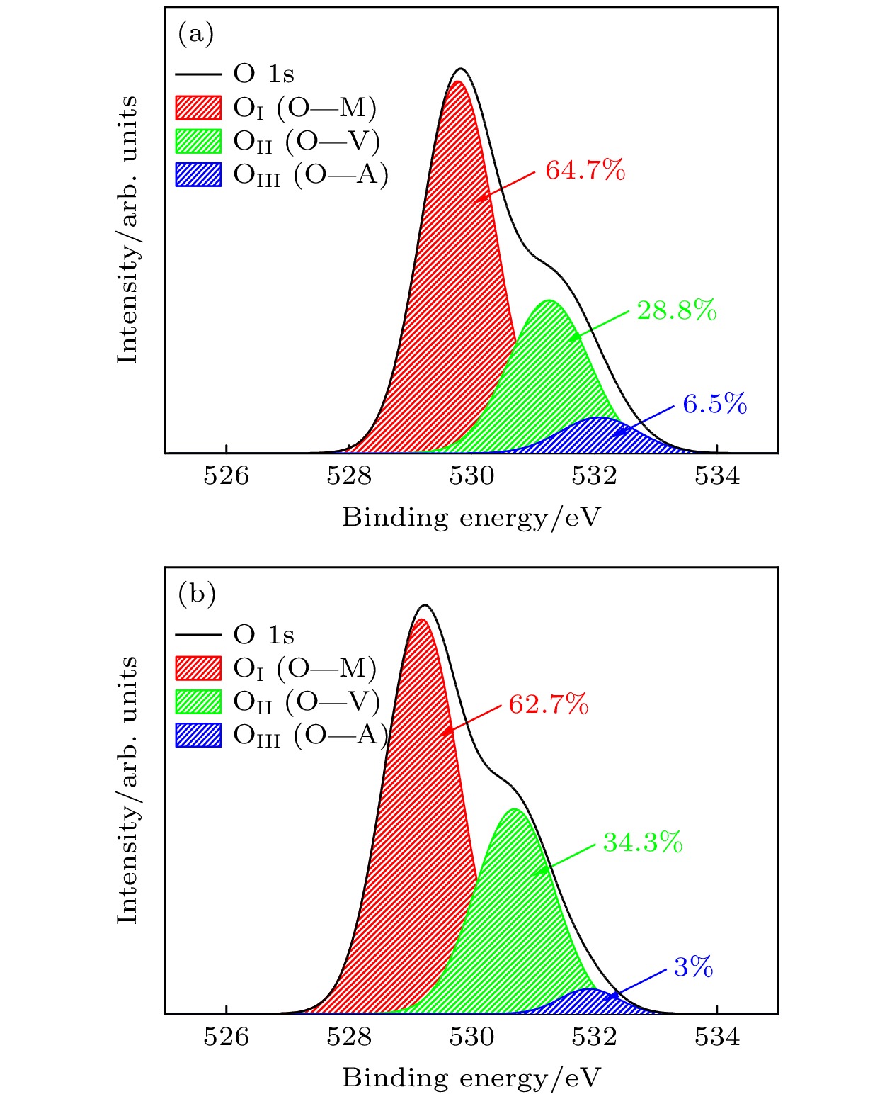
图 7 In2O3薄膜O 1s的拟合XPS图谱 (a)样品1 (传统热退火方式); (b)样品2 (脉冲紫外线辅助热退火方式)
Figure 7. O 1s high resolution XPS spectra of In2O3 thin film: (a) Sample 1 (T.A.); (b) Sample 2 (pulsed UV+T.A.).

图 8 脉冲紫外线辅助热退火促使In2O3薄膜内部氧空位生成机理
Figure 8. Pulsed UV-assisted thermal annealing promotes the mechanism of oxygen vacancy generation inside In2O3 thin films.

图 9 不同退火方式所制备In2O3薄膜的电气特性变化
Figure 9. Variation of electrical properties of In2O3 thin films prepared by different annealing methods.

图 10 不同退火方式所制备样品的(a)输出特性和(b)转移特性
Figure 10. (a) Output and (b) transfer characteristics of samples prepared by different annealing methods.
表 1 不同热退火方式制备In2O3 TFTs的电学特性参数
Table 1. Electrical parameters of In2O3 TFTs prepared by different thermal annealing methods.
样品 亚阈值摆幅 电流比 阈值电压 迁移率 S.S./(mV·dec–1) Ion/Ioff VTH/V μsat/(cm2·V–1·s–1) 样品1 (T.A.) 0.17 1.88×10⁶ 7.6 0.22 样品2 (Pulsed UV +T.A.-5 min) 0.12 1.29×10⁷ 7.4 1.27 样品3 (Pulsed UV +T.A.-10 min) — -2.52 2.43  DownLoad: CSV
-
[1] He Y L, Wang X Y, Gao Y, Hou Y H, Wan Q 2018 J. Semicond. 39 011005
Google Scholar
[2] Zhou Y, Roy V A L, Xu Z X, Kwong H Y, Wang H B, Lee C S 2011 Appl. Phys. Lett. 98 092904
Google Scholar
[3] Liang K, Wang Y, Shao S S, Luo M M, Pecunia V, Shao L, Zhao J W, Chen Z, Mo L X, Cui Z 2019 J. Mater. Chem. C 7 6169
Google Scholar
[4] Kim S J, Yoon S H, Kim H J 2014 J. Appl. Phys. 53 02BA02
Google Scholar
[5] Choi C H, Han S Y, Su Y W, Fang Z, Lin L Y, Cheng C C, Chang C H 2015 J. Mater. Chem. C 3 854
Google Scholar
[6] Kim M G, Kanatzidis M G, Facchetti A, Marks T J 2011 Nat. Mater. 10 382
Google Scholar
[7] Hwang Y H, Seo J S, Yun J M, Park H J, Yang S H, Park S H K, Bae B S 2013 NPG Asia Mater. 5 e45
Google Scholar
[8] Lee H J, Jyothi C, Baang S K , Kwon J H, Bae J H 2016 J. Korean. Phys. Soc. 69 1688
Google Scholar
[9] Zhang X, Lee H J, Kwon J H, Kim E J, Park J H 2017 Materials 10 880
Google Scholar
[10] Park J H, Park W, Na J H, Lee J U, Eun J S, Feng J H, Kim D K, Bae J H 2023 Nanomaterials 13 2568
Google Scholar
[11] 谢应涛, 蔡坤林, 陈鹏龙, 刘愈, 王东平 2022 中国激光 49 0703001
Google Scholar
Xie Y T, Cai K L, Chen P L, Liu Y, Wang D P 2022 Chin. J. Lasers 49 0703001
Google Scholar
[12] Kim W G, Tak Y J, Ahn B D, Jung T S, Chung K B, Kim H J 2016 Sci. Rep. 6 23039
Google Scholar
[13] Rahman M K, Lu Z, Kwon K S 2018 AIP Adv. 8 095008
Google Scholar
[14] Lee H W, Choi H S, Cho W J 2019 J. Nanosci. Nanotechno. 19 6164
Google Scholar
[15] Huang H Y, Wang S J, Wu C H, Lu C Y 2014 Electron. Mater. Lett. 10 899
Google Scholar
[16] Kim D W, Park J H, Hwang J U, Kim H D, Ryu J H, Lee K B, Baek K H, Do L M, Choi J S 2015 Electron. Mater. Lett. 11 82
Google Scholar
[17] Park S C, Kim D W, Shin H J, Lee D K, Zhang X, Park J H, Choi J S 2016 J. Inf. Disp. 17 179
Google Scholar
[18] Huet K, Aubin J, Raynal P E, Curvers B, Verstraete A, Lespinasse B, Mazzamuto F, Sciuto A, Lombardo S F, Magna A L, Acosta-Alba P, Dagault L, Licitra C, Hartmann J M, Kerdilès S 2020 Appl. Surf. Sci. 505 144470
Google Scholar
[19] Lee H J, Zhang X, Kim J W, Kim E J, Park J H 2018 Materials 11 2103
Google Scholar
[20] Azianty S, Saadah A R, Boon T G 2018 Mater. Today 5 S186
Google Scholar
[21] Xing R Q, Xu L, Song J, Zhou C Y, Li Q L, Liu D L, Song H W 2015 Sci. Rep. 5 10717
Google Scholar
[22] Tetzner K, Isakov I, Regoutz A, Payne D J, Anthopoulos T D 2017 J. Mater. Chem. C 5 59
Google Scholar
[23] Shinde D, Ahn D Y, Jadhav V, Lee D Y, Shrestha N K, Lee J K, Lee H, Mane R S, Han S H 2014 J. Mater. Chem. A 2 5490
Google Scholar
[24] Lin Y H, Liu Y S, Lin Y C, Wei Y S, Liao K S, Lee K R, Lai J Y, Chen H M, Jean Y C, Liu C Y 2013 J. Appl. Phys. 113 033706
Google Scholar
[25] Ide K, Nomura K, Hosono H, Kamiya T 2019 Phys. Status Solidi A 216 1800372
Google Scholar
[26] Biswas P, Ainabayev A, Zhussupbekova A, Jose F, O’Connor R, Kaisha A, Walls B, Shvets I V 2020 Sci. Rep. 10 7463
Google Scholar
[27] Tsay C Y, Liang S C 2017 Mat. Sci. Semicon. Proc. 71 441
Google Scholar


 DownLoad:


Catalog
Metrics
- Abstract views: 6272
- PDF Downloads: 79
- Cited By: 0
