-
High-resolution three-dimensional (3D) micro-/nano-fabrication techniques form an important basis for developing the modern micro-/nano-photonics. In this paper, we systematically introduce a new 3D micro-/nano-fabrication technique named as nano-kirigami, which is based on the focused ion beam (FIB) induced in-situ “cutting” and “folding” of a suspended gold film. The high-dose FIB milling fulfils the “cutting” process, and the low-dose FIB irradiation of the effective sample area acts as a mean of “folding”, well representing the fabrication principle of macro-kirigami. By utilizing the topography-guided stress equilibrium during FIB irradiation, nano-kirigami can reliably achieve rich 3D shape transformations, such as multi-directional folding, bending, buckling and twisting, with resolution down to below 50 nm. Taking the FIB-induced stress as a stimulus, the FIB-based nano-kirigami can be divided into “tree-type” and “closed-loop” fabrication from the perspective of topological classifications in multibody dynamics. The characteristics, advantages and disadvantages between the two different types of processes are analyzed and summarized in the paper. The rich 3D shape deformation characteristics bring about unimaginable possibilities for the fabrication of various novel 3D structures, and the generation of new geometries facilitates the exploration of new physics. For example, by taking advantage of the 3D plasmonic conductive couplings, the composite symmetry-broken SRR-based configuration is constructed for the efficient generation of significant chiral Fano resonances. Moreover, with the close-loop nano-kirigami induced by FIB global irradiation, the giant intrinsic optical chirality is achieved in a 3D pinwheel-like structure with exotic twisting and rotation geometric features. Especially, the rotation of the linear polarization direction, caused by the circular birefringence, reaches an efficiency of 310000°/mm which exceeds the reported value of chiral metamaterial and congeneric two-dimensional planar nanostructure. Another example is the metasurface formed by alternately arranging the left-handed pinwheel structure and right-handed pinwheel structure in the horizontal plane, which can diffract cross-polarized transmitted light efficiently while clear photon spin Hall effect is observed. The introduced nano-kirigami technique, as well as the generated exotic 3D nanostructures and their photonic applications, can build up a novel 3D miro-/nano-fabrication platform for versatile structural geometries with promising functionalities, which may find great potential applications in areas such as micro-/nano-photonics, electronic and magnetic devices, plasmonics, optomechanics, micro-/nano-electromechanical systems, etc. -
Keywords:
- three-dimensional micro-/nano-fabrication /
- nano-kirigami /
- focused ion beam /
- optical chirality
[1] 中国剪纸, 百度百科 https://baike.baidu.com/item/%E4%B8%AD%E5%9B%BD%E5%89%AA%E7%BA%B8/397259?fromtitle=%E5%89%AA%E7%BA%B8&fromid=28949&fr=aladdin[2019-10-28]
[2] Chinese paper cutting, Wikipedia https://en.wikipedia.org/wiki/Chinese_paper_cutting [2019-10-28]
[3] History of Origami, Origami Resource Center https://www.origami-resource-center.com/history-of-origami.html[2019-10-28]
[4] Chinese paper folding, Wikipedia https://en.wikipedia.org/wiki/Chinese_paper_folding [2019-10-28]
[5] Kirigami, Wikipedia https://en.wikipedia.org/wiki/Kirigami[2019-10-28]
[6] Wang Z, Jing L, Yao K, Yang Y, Zheng B, Soukoulis C M, Chen H, Liu Y 2017 Adv. Mater. 29 1700412
 Google Scholar
[7] Rogers J, Huang Y, Schmidt O G, Gracias D H 2016 Mrs Bull. 41 123
 Google Scholar
[8] Lamoureux A, Lee K, Shlian M, Forrest S R, Shtein M 2015 Nat. Commun. 6 8092
 Google Scholar
[9] Silverberg J L, Evans A A, McLeod L, Hayward R C, Hull T, Santangelo C D, Cohen I 2014 Science 345 647
 Google Scholar
[10] Zirbel S A, Lang R J, Thomson M W, Sigel D A, Walkemeyer P E, Trease B P, Magleby S P, Howell L L 2013 J. Mech. Design 135 111005
 Google Scholar
[11] Deng J, Ji H, Yan C, Zhang J, Si W, Baunack S, Oswald S, Mei Y, Schmidt O G 2013 Angew. Chem. Int. Edit. 52 2326
 Google Scholar
[12] Kuribayashi K, Tsuchiya K, You Z, Tomus D, Umemoto M, Ito T, Sasaki M 2006 Mater. Sci. Eng. A 419 131
 Google Scholar
[13] Blees M K, Barnard A W, Rose P A, Roberts S P, McGill K L, Huang P Y, Ruyack A R, Kevek J W, Kobrin B, Muller D A, McEuen P L 2015 Nature 524 204
 Google Scholar
[14] Yasuda H, Chong C, Charalampidis E G, Kevrekidis P G, Yang J 2016 Phys. Rev. E 93 043004
 Google Scholar
[15] Momeni F, Hassani S M M N, Liu X, Ni J 2017 Mater. Design 122 42
 Google Scholar
[16] Zhang Y, Zhang F, Yan Z, Ma Q, Li X, Huang Y, Rogers J A 2017 Nat. Rev. Mater. 2 17019
 Google Scholar
[17] Zhang Y, Yan Z, Nan K, Xiao D, Liu Y, Luan H, Fu H, Wang X, Yang Q, Wang J, Ren W, Si H, Liu F, Yang L, Li H, Wang J, Guo X, Luo H, Wang L, Huang Y, Rogers J A 2015 Proc. Natl. Acad. Sci. U. S. A. 112 11757
 Google Scholar
[18] Cui J, Adams J G M, Zhu Y 2017 Smart Mater. Struct. 26 125011
 Google Scholar
[19] Liu N, Guo H, Fu L, Kaiser S, Schweizer H, Giessen H 2008 Nat. Mater. 7 31
 Google Scholar
[20] Gansel J K, Thiel M, Rill M S, Decker M, Bade K, Saile V, Von Freymann G, Linden S, Wegener M 2009 Science 325 1513
 Google Scholar
[21] Turner M D, Saba M, Zhang Q, Cumming B P, Schroeder Turk G E, Gu M 2013 Nat. Photonics 7 801
 Google Scholar
[22] Syms R R A, Yeatman E M 1993 Electron. Lett. 29 662
 Google Scholar
[23] Syms R R A 1995 J. Microelectromech. S. 4 177
 Google Scholar
[24] Syms R R A, Yeatman E M, Bright V M, Whitesides G M 2003 J. Microelectromech. S. 12 387
 Google Scholar
[25] Cho J H, Keung M D, Verellen N, Lagae L, Moshchalkov V V, van Dorpe P, Gracias D H 2011 Small 7 1943
 Google Scholar
[26] Pandey S, Ewing M, Kunas A, Nguyen N, Gracias D H, Menon G 2011 Proc. Natl. Acad. Sci. U. S. A. 108 19885
 Google Scholar
[27] Prinz V Y, Seleznev V A, Gutakovsky A K, Chehovskiy A V, Preobrazhenskii V V, Putyato M A, Gavrilova T A 2000 Physica E 6 828
 Google Scholar
[28] Schmidt O G, Eberl K 2001 Nature 410 168
 Google Scholar
[29] Li X L 2008 J. Phys. D.: Appl. Phys. 41 193001
 Google Scholar
[30] Li X L 2011 Adv. Opt. Photonics 3 366
 Google Scholar
[31] Klein Y, Efrati E, Sharon E 2007 Science 315 1116
 Google Scholar
[32] Kim J, Hanna J A, Byun M, Santangelo C D, Hayward R C 2012 Science 335 1201
 Google Scholar
[33] Na J H, Evans A A, Bae J, Chiappelli M C, Santangelo C D, Lang R J, Hull T C, Hayward R C 2015 Adv. Mater. 27 79
 Google Scholar
[34] Na J H, Bende N P, Bae J, Santangelo C D, Hayward R C 2016 Soft Matter 12 4985
 Google Scholar
[35] Palleau E, Morales D, Dickey M D, Velev O D 2013 Nat. Commun. 4 2257
 Google Scholar
[36] Wu Z L, Moshe M, Greener J, Therien Aubin H, Nie Z, Sharon E, Kumacheva E 2013 Nat. Commun. 4 1586
 Google Scholar
[37] Chalapat K, Chekurov N, Jiang H, Li J, Parviz B, Paraoanu G S 2013 Adv. Mater. 25 91
 Google Scholar
[38] Jamal M, Zarafshar A M, Gracias D H 2011 Nat. Commun. 2 527
 Google Scholar
[39] Xu S, Yan Z, Jang K I, Huang W, Fu H, Kim J, Wei Z, Flavin M, McCracken J, Wang R, Badea A, Liu Y, Xiao D, Zhou G, Lee J, Chung H U, Cheng H, Ren W, Banks A, Li X, Paik U, Nuzzo R G, Huang Y, Zhang Y, Rogers J A 2015 Science 347 154
 Google Scholar
[40] Chen H, Zhang X L, Zhang Y Y, Wang D, Bao D L, Que Y, Xiao W, Du S, Ouyang M, Pantelides S T, Gao H J 2019 Science 365 1036
 Google Scholar
[41] 刘之光 2019 博士学位论文 (北京: 中国科学院大学)
Liu Z G 2019 Ph. D. Dissertation (Beijing: Chinese Academy of Sciences) (in Chinese)
[42] Li J F, Liu Z G 2018 Nanophotonics 7 1637
 Google Scholar
[43] Liu Z, Du H, Li J, Lu L, Li Z Y, Fang N X 2018 Sci. Adv. 4 4436
 Google Scholar
[44] Arora W J, Smith H I, Barbastathis G 2007 Microelectron. Eng. 84 1454
 Google Scholar
[45] Samayoa M J, Haque M A, Cohen P H 2008 J. Micromech. Microeng. 18 095005
 Google Scholar
[46] Nix W D, Clemens B M 1999 J. Mater. Res. 14 3467
 Google Scholar
[47] Melngailis J 1987 J. Vac. Sci. Technol. B 5 469
[48] Sugiyama M, Sigesato G 2004 J. Electron Microsc. 53 527
 Google Scholar
[49] Yoshida T, Baba A, Asano T 2005 Jap. J. Appl. Phys. 44 5744
 Google Scholar
[50] Park B C, Jung K Y, Song W Y, Beom-hoan O, Ahn S J 2006 Adv. Mater. 18 95
 Google Scholar
[51] Xia L, Wu W G, Xu J, Hao Y L, Wang Y Y 2006 19th IEEE International Conference on Micro Electro Mechanical Systems Istanbul, Turkey, January 22−26, 2006 p118
[52] Arora W J, Sijbrandij S, Stern L, Notte J, Smith H I, Barbastathis G 2007 J. Vac. Sci. Technol. B. 25 2184
 Google Scholar
[53] Arora W J, Sijbrandij S, Stern L, Notte J, Smith H I, Barbastathis G 2007 J. Vac. Sci. Technol. B 25 2184
[54] Yoshida T, Nagao M, Kanemaru S 2010 Jap. J. Appl. Phys. 49 056501
 Google Scholar
[55] Chalapat K, Chekurov N, Li J, Paraoanu G S 2012 Nucl. Instrum. Meth. B 272 202
 Google Scholar
[56] Punzhin S, Detsi E, Kuzmin A, de Hosson J T M 2014 J. Mater. Sci. 49 5598
 Google Scholar
[57] Cui A, Liu Z, Li J, Shen T H, Xia X, Li Z, Gong Z, Li H, Wang B, Li J, Yang H, Li W, Gu C 2015 Light Sci. Appl. 4 308
 Google Scholar
[58] Liu Z, Liu Z, Li J, Li W, Li J, Gu C, Li Z Y 2016 Sci. Rep. UK 6 27817
 Google Scholar
[59] Mao Y, Pan Y, Zhang W, Zhu R, Xu J, Wu W 2016 Nano Lett. 16 7025
 Google Scholar
[60] Liu Z, Li J, Liu Z, Li W, Li J, Gu C, Li Z Y 2017 Sci. Rep. UK 7 8010
 Google Scholar
[61] Tian X, Liu Z, Lin H, Jia B, Li Z Y, Li J 2018 Nanoscale 10 16630
 Google Scholar
[62] Yang S Y, Liu Z, Hu S, Jin A Z, Yang H F, Zhang S, Li J J, Gu C Z 2019 Nano Lett. 19 3432
 Google Scholar
[63] Yang S, Zhe L, Ling J, Li W, Shuang Z, Li J, Gu C 2017 ACS Photonics 4 2650
 Google Scholar
[64] Antonio T, Claudio M 1996 Modelling and Control of Mechanisms and Robots (Singapore and London: World Scientific) p55
[65] Buchner T 2003 Ph. D. Dissertation (Boston: Massachusetts Institute of Technology) (in America)
[66] Liu Z, Du H, Li Z Y, Fang N X, Li J 2018 Apl. Photonics 3 100803
 Google Scholar
[67] Rajput N S, Banerjee A, Verma H C 2011 Nanotechnology 22 485302
 Google Scholar
[68] Mao Y, Zheng Y, Li C, Guo L, Pan Y, Zhu R, Xu J, Zhang W, Wu W 2017 Adv. Mater. 29 1606482
 Google Scholar
[69] Wu C H, Khanikaev A B, Adato R, Arju N, Yanik A A, Altug H, Shvets G 2012 Nat. Mater. 11 69
 Google Scholar
[70] Plum E, Liu X X, Fedotov V A, Chen Y, Tsai D P, Zheludev N I 2009 Phys. Rev. Lett. 102 113902
 Google Scholar
[71] Wang Z, Cheng F, Winsor T, Liu Y 2016 Nanotechnology 27 412001
 Google Scholar
[72] Zhao R, Zhang L, Zhou J, Koschny T, Soukoulis C M 2011 Phys. Rev. B 83 035105
 Google Scholar
[73] Rodrigues S P, Lan S F, Kang L, Cui Y H, Panuski P W, Wang S X, Urbas A M, Cai W S 2017 Nat. Commun. 8 14602
 Google Scholar
[74] Hentschel M, Schaferling M, Duan X Y, Giessen H, Liu N 2017 Sci. Adv. 3 1602735
 Google Scholar
[75] Zhang S, Park Y S, Li J S, Lu X C, Zhang W L, Zhang X 2009 Phys. Rev. Lett. 102 023901
 Google Scholar
[76] Zhu A Y, Chen W T, Zaidi A, Huang Y W, Khorasaninejad M, Sanjeev V, Qiu C W, Capasso F 2018 Light Sci. Appl. 7 17158
 Google Scholar
[77] Onoda S, Murakami S, Nagaosa N 2004 Phys. Rev. Lett. 93 167602
 Google Scholar
[78] Yin X B, Ye Z L, Rho J, Wang Y, Zhang X 2013 Science 339 1405
 Google Scholar
[79] Ling X H, Zhou X X, Huang K, Liu Y C, Qiu C W, Luo H L, Wen S C 2017 Rep. Prog. Phys. 80 066401
 Google Scholar
[80] Bliokh K Y, Niv A, Kleiner V, Hasman E 2008 Nat. Photonics 2 748
 Google Scholar
-
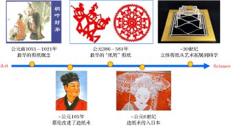
图 1 剪纸从艺术到科学的发展(从左到右依次为《史记》典故“剪桐封弟”[1], 又称“桐叶封弟”; 约公元105年蔡伦改进了造纸术[4]; 中国发现的最早的剪纸文物“北朝对马团花剪纸”残片与复原图[1]; 纸文化在公元6世纪左右传播到日本[3]; 2015年发表的石墨烯剪纸技术[13])
Figure 1. Development of paper-cutting from art to science (From left to right: the recorded historical allusion around 1055–1021 B.C.[1]; the improvement of paper manufacturing by Cai Lun around 105 A.D.[4]; the earliest relic of the paper-cuts named “Flowery Horses” around 386–581 A.D.[1]; the spread of paper to Japan during the 6th century[3]; graphene kirigami published in 2015[13]).
图 2 (a)−(d) 常见的形变应力产生的三种机制及其对应的实例[16,26,28,32,37,38]: 从(b)到(d)依次为毛细作用力、薄膜残余应力和主动材料法; (e) 机械引导结构变形流程及结构图[39]; (f) 石墨烯剪纸[13]; (g)石墨烯纳米折叠和展开[40]
Figure 2. (a)−(d) Illustration of several deformation stresses and corresponding examples[16,26,28,32,37,38]; (b) capillary forces; (c) film residual stresses; (d) active materials induced forces; (e) illustration of the mechanically guided assembly[39]; (f) graphene kirigami[13]; (g) graphene origami[40]
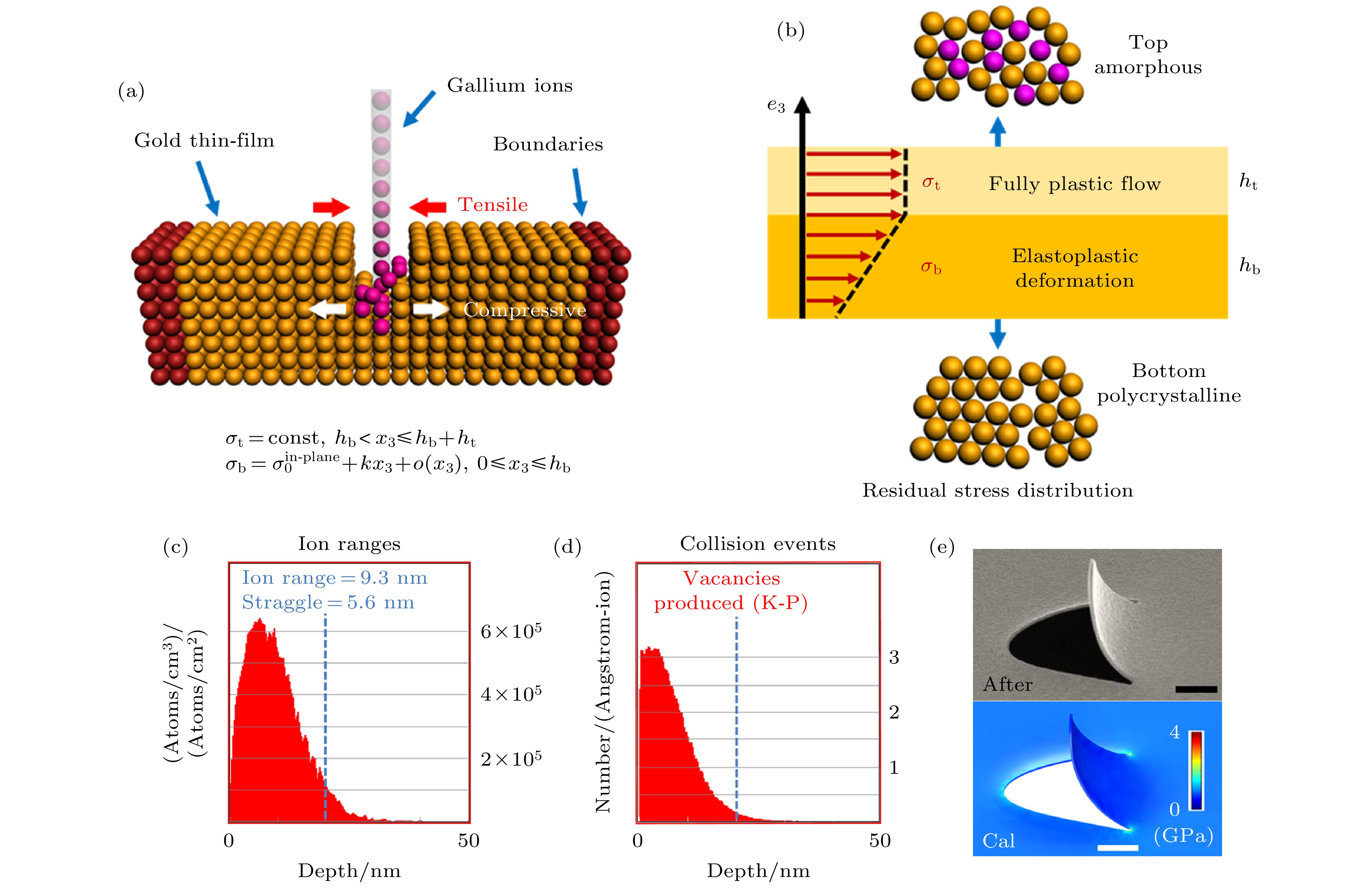
图 3 基于FIB辐照产生应力的主要机理[43] (a), (b)自支撑金膜在FIB辐照下的应力分布和双层应力模型示意图; 利用SRIM软件计算得到的在加速电压为30 kV时(c)镓离子和(d)空隙的深度分布图; (e)舌型结构在FIB全局辐照后的扫描电子显微镜 (scanning electron microscopy, SEM)图像和利用(b)图中双层应力模型计算的结果(比例尺: 1 μm)
Figure 3. Illustration of the fundamentals of FIB-induced stress[43]: (a), (b) Schematic illustration of residual stress distribution and double-layer stress model within a gold nano-film under FIB irradiation; simulated distributions of (c) gallium ion concentration and (d) vacancy density versus the depth of the nanofilm using SRIM software with ion acceleration voltage of 30 kV; (e) SEM image of a tongue-like structure after FIB global irradiation and the calculated result (Scale bars: 1 μm).
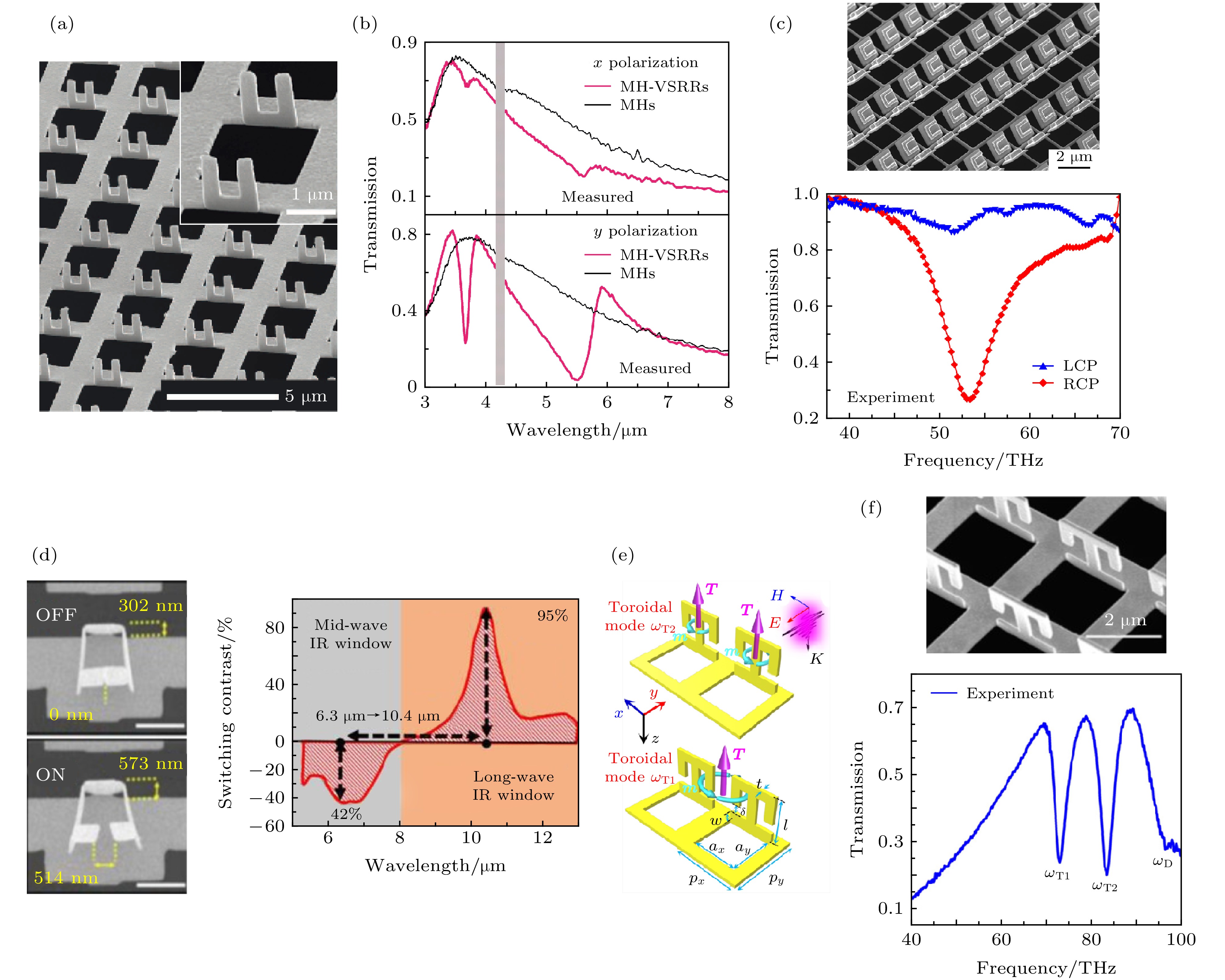
图 5 (a), (b)垂直开口谐振环(VSRR)与金属矩形孔组成的复合结构(MH-VSRR)阵列及其偏振相关Fano共振[57]; (c)三维折叠超表面的SEM图像以及右旋圆偏振光(RCP)和左旋圆偏光(LCP)的透射光谱[61]; (d)可调的三维SRR分别处于OFF和ON态时的SEM图像, 及纳米SRR阵列的开关光谱特性[59]; (e)环形偶极子模式的示意图[63]; (f)三维超材料SEM图片及透射图光谱[63]
Figure 5. (a), (b) Composite structure (MH-VSRR) prepared by FIB and the polarization-dependent Fano resonance[57]; (c) SEM image of 3D folded metasurface and experimentally measured transmission spectra under illumination of different circularly polarized waves[61]; (d) SEM images of switchable 3D SRR[59] in OFF and ON states at currents of 0 and 20 mA, respectively, and corresponding switching spectra; (e) schematic of toroidal dipole modes generated due to circulating magnetic field produced by current loops[63]; (f) SEM image of the 3D toroidal metamaterial and the measured transmission spectra with toroidal dipole resonance dips[63].
图 6 (a) FIB局域扫描红色虚线、折叠悬臂的SEM图[42]; (b) FIB全局辐照红色虚线框内区域导致悬臂向上弯曲的SEM图[42]; (c)测量得到的不同加速电压下悬臂梁折叠角与扫描剂量的关系[43]; (d)不同尺寸的悬臂在不同剂量FIB全局扫描下弯曲的SEM图像[43]; (e)测量(点线)与计算(实线)得到的在加速电压为30 kV时不同长度悬臂梁的折叠角与扫描剂量的关系[43](比例尺: 1 μm)
Figure 6. Side-view SEM images of (a) rigid folding and (b) gradual bending of suspended cantilevers under local and global FIB irradiations, respectively, over the red areas [42]; (c) measured relationship between the cantilever folding angle and the scanning dose at different acceleration voltages[43]; (d) SEM images of different sizes of cantilever bending under FIB global irradiation with different dose[43]; (e) measured (dotted line) and calculated (solid line) relationship between the folding angle and the scanning dose at acceleration voltage of 30 kV[43] (Scale bars: 1 μm).
图 7 “树型”纳米剪纸 (a)“树型”纳米剪纸结构示意图; (b)—(f)“树型”纳米剪纸结构SEM图像, 其中 (b), (c)为由FIB全局辐照得到的两种花瓣型结构[42,66]; (d)−(f)为由FIB局域辐照得到结构的SEM图片, (d), (e)垂直矩形板阵列的侧视图和俯视图[42]; (f)多层平板结构[42](比例尺: 1 μm)
Figure 7. Tree-type nano-kirigami: (a) Schematic of tree-type system; (b)−(f) SEM images of typical examples of 3D tree-type nano-kirigami. (b), (c) Flower-like structures obtained by FIB global irradiation[42,66]; (d), (e) side-view and top-view of vertical plates standing along one edge of the planar metallic hole arrays[42]; (f) multilayer plate structure[42] (Scale bars: 1 μm).
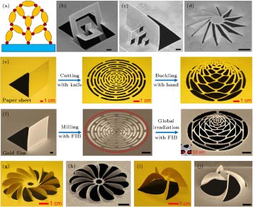
图 8 “闭环”纳米剪纸[42,43] (a)“闭环”纳米剪纸结构示意图; (b)−(d)由FIB局域辐照下“闭环”纳米剪纸得到的三维纳米结构的SEM图像[42]; (e), (g), (i)宏观纸质剪纸结构照片及与其对应的(f), (h), (j)通过FIB全局扫描“闭环”纳米剪纸得到的三维纳米结构的SEM图像[43] (比例尺: 1 μm)
Figure 8. Close-loop of nano-kirigami[42,43]: (a) Illustration of the close-loop system; (b)−(d) SEM images of 3D nano-kirigami with local FIB irradiation[42]; (e), (g), (i) camera images of the macroscopic paper kirigami; and (f), (h), (j) corresponding microscopic structures reproduced by close-loop nano-kirigami with global FIB irradiation[43] (Scale bars: 1 μm).
图 9 各种形貌奇特的三维纳米剪纸结构在FIB全局扫描前后的顶视或侧视SEM图[43] (a) 斐波那契双螺旋结构; (b), (c)窗花互连型纳米栅栏; (d)不同剂量FIB辐照前后的螺旋结构; (e)双层螺旋异质结构(比例尺: 1 μm)
Figure 9. Top-view and side-view SEM images of typical structures before and after global FIB irradiation[43]: (a) A twisted triple Fibonacci spiral; (b), (c) window-decoration type nanobarriers; (d) a deformable spiral; (e) a double-layer spiral structure (Scale bars: 1 μm).
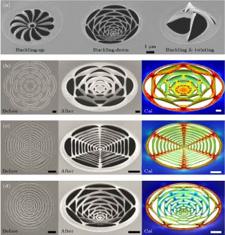
图 10 “闭环”纳米剪纸的形变特性[43] (a)叶片结构、可扩展网状结构和四臂风车结构在其二维前体受到相同FIB全局辐照后的SEM图像; (b)−(d) FIB全局辐照前后的二维前体和对应的三维结构以及数值模拟的应力形变结果, 其中 (b)花型结构, (c)蛛网结构, (d)可扩展网状结构(比例尺: 1 μm)
Figure 10. Feature of “closed loop” nano-kirigami[43]: (a) SEM images of a blade structure, expandable web and four-arm windmill fabricated together after the same global FIB irradiation; (b)−(d) SEM images of different web structures (left) before and (middle) after FIB irradiation; (b) a flower-like structure; (c) a spider web–like structure; (d) an expandable web structure; the simulation results after nano-kirigami is shown on the right (Scale bars: 1 μm).
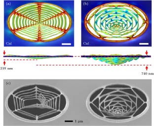
图 11 数值模拟对结构形变的精确预测与额外信息获取[43] (a), (b)数值模拟蛛网结构和可扩展网状结构在相同FIB辐照下受力形变的侧视图和前视图, 其中不同的颜色代表受到不同强度的应力, 红色区域承受的应力最大(比例尺: 1 μm); (c)两种结构承受相同FIB扫描后的SEM图
Figure 11. Additional information from numerical simulation for the accurate prediction of structural deformation[43]: (a), (b) Side and front view of the deformation and stress distribution of the spider web-like and the expandable web structure under the same initial stress in simulations; the different colors represent stresses of different strengths, and the red areas are subjected to the highest stress (Scale bars: 1 μm); (c) SEM image of the two web structures after the same high-dose FIB irradiation.
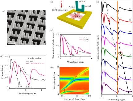
图 12 具有Fano共振的“树型”纳米剪纸[57,60] (a), (b)近红外波段Fano共振及超灵敏折射率传感特性[57], 其中(a) MH-VSRR阵列结构的SEM图及(b)测得的结构在空气和折射率为1.3的油中的透射谱; (c)−(e)纳米剪纸结构中多重Fano共振间的强耦合作用[60], 其中(c)不对称MH-VSRR单元结构图及(d)结构所对应的透射光谱, 可以看到三重Fano共振F1, F2和F3; (e)固定左臂、改变右臂高度时MH-VSRR结构透射谱; (f)结构吸收谱与右臂高度的关系图, 理论和实验数据吻合得非常好
Figure 12. Tree-type nano-kirigami structures with Fano resonances[57,60]: (a) SEM images of MH-VSRR[57]; (b) measured transmission spectra of the MH-VSRR array in air and oil; (c) schematic of the unit cell of a 3D asymmetric MH-VSRR[60]; (d) simulated transmission spectra of the asymmetric MH-VSRR array[60]; (e) simulated transmission spectra of the VSRR with the same left arm but variable right arm as noted; (f) colormap of the simulated absorption spectra versus the height of the right arm; the calculated (dashed lines) and measured data (stars) agree very well.
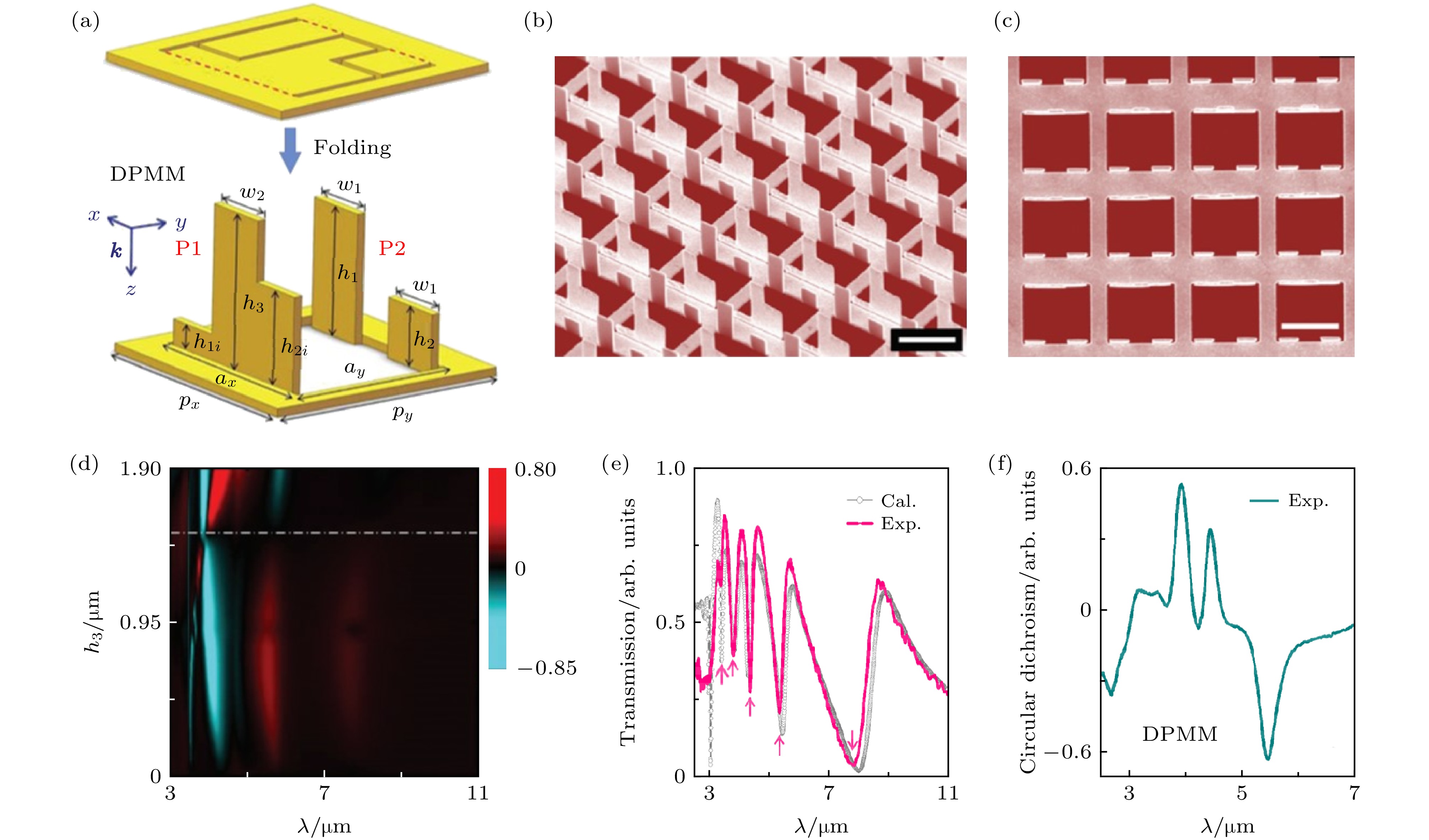
图 13 具有超强圆二色性的五重Fano共振[61] (a)基于竖直金属板的超材料(DPMM)结构加工示意图; (b), (c) FIB局域扫描制备的DPMM阵列结构的侧视和顶视SEM图像(比例尺: 2 μm); (d)模拟的DPMM阵列圆二色谱与h3的关系图; (e) h3取1.9 μm, y偏振入射时计算和实验得到的透射谱; (f)实验测量的h3取1.9 μm时的CD谱
Figure 13. Five-fold Fano resonance with significant circular dichroism[61]: (a) Schematic diagram of the processing of DPMM; (b), (c) SEM images of DPMM structures prepared by FIB local irradiation (Scale bars: 2 μm); (d) diagram of the relationship between CD and h3 of simulated DPMM; (e) calculated and experimental transmission spectra for the DPMM with h3 = 1.9 μm and y-polarized incidence; (f) experimental CD spectra of the DPMM in (e).
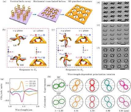
图 14 “闭环”纳米剪纸光学超手征特性[43] (a)从螺旋结构到三维风车结构的设计演化示意图; (b), (c) LH风车结构和RH风车结构对入射光电场分量Ex和磁场分量Hy响应的示意图; (d), (e)三维风车结构及二维前体SEM图像, 晶格周期为1.45 μm; (f) LH及RH三维风车结构SEM顶视图; (g)二维LH、三维LH和三维RH结构透射的CD谱; (h)不同波长处三维风车结构的线偏振旋转极坐标图
Figure 14. Close-loop nano-kirigami with giant optical chirality[43]: (a) Schematic of a vertical helix array, horizontal cross-linked helices and a 3D pinwheel array; (b), (c) illustrations of the response to the electric field (Ex) and magnetic field (Hy) of incident light for the left-handed (LH) and right-handed (RH) twisted pinwheels, respectively; (d), (e) SEM images of LH pinwheel arrays (e) before and (d) after global FIB irradiation; lattice period: 1.45 μm; (f) SEM images of the LH and RH pinwheel structure; (g) measured CD in transmission versus wavelength for 2D LH, 3D LH, and 3D RH pinwheels, respectively; (h) measured and calculated linear polarization rotation angle versus wavelength for 2D and 3D LH pinwheels.
图 15 “闭环”纳米剪纸超构表面[66] (a)不同手性结构交叉偏振透射相位光谱; (b)由不同手性风车结构交替排列组成的二元线性光栅(比例尺: 1 μm); (c)由不同手性风车结构交替排列组成的圆形二元光栅的SEM图(比例尺: 10 μm); (d)线性二元光栅对透射光偏振调制示意图; (e)不同波长和探测偏振下二元线性光栅透射实验照片, 入射光为x偏振; (f)−(h)二元线性光栅对圆偏振光的调制; (i)−(m)不同波长和探测偏振下的圆形二元光栅的实验照片(比例尺: 10 μm)
Figure 15. Metasurface by “closed-loop” nano-kirigami[66]: (a) Transmission phase spectra of Ey for LH and RH pinwheels, respectively; (b) top-view SEM image of a linear grating in which the LH and RH pinwheels are fabricated alternately along the x-direction; scale bar, 1 μm; (c) top-view SEM image of a circular grating; scale bar, 10 μm; (d) schematic of the diffraction properties of the linear grating; (e) CCD camera images of the transmitted light spots at different wavelengths under detection with no polarization (np), x-polarization (xp), and y-polarization (yp), respectively; (f)−(h) CCD images of the spots of the diffracted (left) RCP and (middle) LCP beams under the illumination with LCP, RCP and x-polarized incident light, respectively; (i)−(m) photographs of circular binary gratings at different wavelengths (Scale bars: 10 μm).
-
[1] 中国剪纸, 百度百科 https://baike.baidu.com/item/%E4%B8%AD%E5%9B%BD%E5%89%AA%E7%BA%B8/397259?fromtitle=%E5%89%AA%E7%BA%B8&fromid=28949&fr=aladdin[2019-10-28]
[2] Chinese paper cutting, Wikipedia https://en.wikipedia.org/wiki/Chinese_paper_cutting [2019-10-28]
[3] History of Origami, Origami Resource Center https://www.origami-resource-center.com/history-of-origami.html[2019-10-28]
[4] Chinese paper folding, Wikipedia https://en.wikipedia.org/wiki/Chinese_paper_folding [2019-10-28]
[5] Kirigami, Wikipedia https://en.wikipedia.org/wiki/Kirigami[2019-10-28]
[6] Wang Z, Jing L, Yao K, Yang Y, Zheng B, Soukoulis C M, Chen H, Liu Y 2017 Adv. Mater. 29 1700412
 Google Scholar
[7] Rogers J, Huang Y, Schmidt O G, Gracias D H 2016 Mrs Bull. 41 123
 Google Scholar
[8] Lamoureux A, Lee K, Shlian M, Forrest S R, Shtein M 2015 Nat. Commun. 6 8092
 Google Scholar
[9] Silverberg J L, Evans A A, McLeod L, Hayward R C, Hull T, Santangelo C D, Cohen I 2014 Science 345 647
 Google Scholar
[10] Zirbel S A, Lang R J, Thomson M W, Sigel D A, Walkemeyer P E, Trease B P, Magleby S P, Howell L L 2013 J. Mech. Design 135 111005
 Google Scholar
[11] Deng J, Ji H, Yan C, Zhang J, Si W, Baunack S, Oswald S, Mei Y, Schmidt O G 2013 Angew. Chem. Int. Edit. 52 2326
 Google Scholar
[12] Kuribayashi K, Tsuchiya K, You Z, Tomus D, Umemoto M, Ito T, Sasaki M 2006 Mater. Sci. Eng. A 419 131
 Google Scholar
[13] Blees M K, Barnard A W, Rose P A, Roberts S P, McGill K L, Huang P Y, Ruyack A R, Kevek J W, Kobrin B, Muller D A, McEuen P L 2015 Nature 524 204
 Google Scholar
[14] Yasuda H, Chong C, Charalampidis E G, Kevrekidis P G, Yang J 2016 Phys. Rev. E 93 043004
 Google Scholar
[15] Momeni F, Hassani S M M N, Liu X, Ni J 2017 Mater. Design 122 42
 Google Scholar
[16] Zhang Y, Zhang F, Yan Z, Ma Q, Li X, Huang Y, Rogers J A 2017 Nat. Rev. Mater. 2 17019
 Google Scholar
[17] Zhang Y, Yan Z, Nan K, Xiao D, Liu Y, Luan H, Fu H, Wang X, Yang Q, Wang J, Ren W, Si H, Liu F, Yang L, Li H, Wang J, Guo X, Luo H, Wang L, Huang Y, Rogers J A 2015 Proc. Natl. Acad. Sci. U. S. A. 112 11757
 Google Scholar
[18] Cui J, Adams J G M, Zhu Y 2017 Smart Mater. Struct. 26 125011
 Google Scholar
[19] Liu N, Guo H, Fu L, Kaiser S, Schweizer H, Giessen H 2008 Nat. Mater. 7 31
 Google Scholar
[20] Gansel J K, Thiel M, Rill M S, Decker M, Bade K, Saile V, Von Freymann G, Linden S, Wegener M 2009 Science 325 1513
 Google Scholar
[21] Turner M D, Saba M, Zhang Q, Cumming B P, Schroeder Turk G E, Gu M 2013 Nat. Photonics 7 801
 Google Scholar
[22] Syms R R A, Yeatman E M 1993 Electron. Lett. 29 662
 Google Scholar
[23] Syms R R A 1995 J. Microelectromech. S. 4 177
 Google Scholar
[24] Syms R R A, Yeatman E M, Bright V M, Whitesides G M 2003 J. Microelectromech. S. 12 387
 Google Scholar
[25] Cho J H, Keung M D, Verellen N, Lagae L, Moshchalkov V V, van Dorpe P, Gracias D H 2011 Small 7 1943
 Google Scholar
[26] Pandey S, Ewing M, Kunas A, Nguyen N, Gracias D H, Menon G 2011 Proc. Natl. Acad. Sci. U. S. A. 108 19885
 Google Scholar
[27] Prinz V Y, Seleznev V A, Gutakovsky A K, Chehovskiy A V, Preobrazhenskii V V, Putyato M A, Gavrilova T A 2000 Physica E 6 828
 Google Scholar
[28] Schmidt O G, Eberl K 2001 Nature 410 168
 Google Scholar
[29] Li X L 2008 J. Phys. D.: Appl. Phys. 41 193001
 Google Scholar
[30] Li X L 2011 Adv. Opt. Photonics 3 366
 Google Scholar
[31] Klein Y, Efrati E, Sharon E 2007 Science 315 1116
 Google Scholar
[32] Kim J, Hanna J A, Byun M, Santangelo C D, Hayward R C 2012 Science 335 1201
 Google Scholar
[33] Na J H, Evans A A, Bae J, Chiappelli M C, Santangelo C D, Lang R J, Hull T C, Hayward R C 2015 Adv. Mater. 27 79
 Google Scholar
[34] Na J H, Bende N P, Bae J, Santangelo C D, Hayward R C 2016 Soft Matter 12 4985
 Google Scholar
[35] Palleau E, Morales D, Dickey M D, Velev O D 2013 Nat. Commun. 4 2257
 Google Scholar
[36] Wu Z L, Moshe M, Greener J, Therien Aubin H, Nie Z, Sharon E, Kumacheva E 2013 Nat. Commun. 4 1586
 Google Scholar
[37] Chalapat K, Chekurov N, Jiang H, Li J, Parviz B, Paraoanu G S 2013 Adv. Mater. 25 91
 Google Scholar
[38] Jamal M, Zarafshar A M, Gracias D H 2011 Nat. Commun. 2 527
 Google Scholar
[39] Xu S, Yan Z, Jang K I, Huang W, Fu H, Kim J, Wei Z, Flavin M, McCracken J, Wang R, Badea A, Liu Y, Xiao D, Zhou G, Lee J, Chung H U, Cheng H, Ren W, Banks A, Li X, Paik U, Nuzzo R G, Huang Y, Zhang Y, Rogers J A 2015 Science 347 154
 Google Scholar
[40] Chen H, Zhang X L, Zhang Y Y, Wang D, Bao D L, Que Y, Xiao W, Du S, Ouyang M, Pantelides S T, Gao H J 2019 Science 365 1036
 Google Scholar
[41] 刘之光 2019 博士学位论文 (北京: 中国科学院大学)
Liu Z G 2019 Ph. D. Dissertation (Beijing: Chinese Academy of Sciences) (in Chinese)
[42] Li J F, Liu Z G 2018 Nanophotonics 7 1637
 Google Scholar
[43] Liu Z, Du H, Li J, Lu L, Li Z Y, Fang N X 2018 Sci. Adv. 4 4436
 Google Scholar
[44] Arora W J, Smith H I, Barbastathis G 2007 Microelectron. Eng. 84 1454
 Google Scholar
[45] Samayoa M J, Haque M A, Cohen P H 2008 J. Micromech. Microeng. 18 095005
 Google Scholar
[46] Nix W D, Clemens B M 1999 J. Mater. Res. 14 3467
 Google Scholar
[47] Melngailis J 1987 J. Vac. Sci. Technol. B 5 469
[48] Sugiyama M, Sigesato G 2004 J. Electron Microsc. 53 527
 Google Scholar
[49] Yoshida T, Baba A, Asano T 2005 Jap. J. Appl. Phys. 44 5744
 Google Scholar
[50] Park B C, Jung K Y, Song W Y, Beom-hoan O, Ahn S J 2006 Adv. Mater. 18 95
 Google Scholar
[51] Xia L, Wu W G, Xu J, Hao Y L, Wang Y Y 2006 19th IEEE International Conference on Micro Electro Mechanical Systems Istanbul, Turkey, January 22−26, 2006 p118
[52] Arora W J, Sijbrandij S, Stern L, Notte J, Smith H I, Barbastathis G 2007 J. Vac. Sci. Technol. B. 25 2184
 Google Scholar
[53] Arora W J, Sijbrandij S, Stern L, Notte J, Smith H I, Barbastathis G 2007 J. Vac. Sci. Technol. B 25 2184
[54] Yoshida T, Nagao M, Kanemaru S 2010 Jap. J. Appl. Phys. 49 056501
 Google Scholar
[55] Chalapat K, Chekurov N, Li J, Paraoanu G S 2012 Nucl. Instrum. Meth. B 272 202
 Google Scholar
[56] Punzhin S, Detsi E, Kuzmin A, de Hosson J T M 2014 J. Mater. Sci. 49 5598
 Google Scholar
[57] Cui A, Liu Z, Li J, Shen T H, Xia X, Li Z, Gong Z, Li H, Wang B, Li J, Yang H, Li W, Gu C 2015 Light Sci. Appl. 4 308
 Google Scholar
[58] Liu Z, Liu Z, Li J, Li W, Li J, Gu C, Li Z Y 2016 Sci. Rep. UK 6 27817
 Google Scholar
[59] Mao Y, Pan Y, Zhang W, Zhu R, Xu J, Wu W 2016 Nano Lett. 16 7025
 Google Scholar
[60] Liu Z, Li J, Liu Z, Li W, Li J, Gu C, Li Z Y 2017 Sci. Rep. UK 7 8010
 Google Scholar
[61] Tian X, Liu Z, Lin H, Jia B, Li Z Y, Li J 2018 Nanoscale 10 16630
 Google Scholar
[62] Yang S Y, Liu Z, Hu S, Jin A Z, Yang H F, Zhang S, Li J J, Gu C Z 2019 Nano Lett. 19 3432
 Google Scholar
[63] Yang S, Zhe L, Ling J, Li W, Shuang Z, Li J, Gu C 2017 ACS Photonics 4 2650
 Google Scholar
[64] Antonio T, Claudio M 1996 Modelling and Control of Mechanisms and Robots (Singapore and London: World Scientific) p55
[65] Buchner T 2003 Ph. D. Dissertation (Boston: Massachusetts Institute of Technology) (in America)
[66] Liu Z, Du H, Li Z Y, Fang N X, Li J 2018 Apl. Photonics 3 100803
 Google Scholar
[67] Rajput N S, Banerjee A, Verma H C 2011 Nanotechnology 22 485302
 Google Scholar
[68] Mao Y, Zheng Y, Li C, Guo L, Pan Y, Zhu R, Xu J, Zhang W, Wu W 2017 Adv. Mater. 29 1606482
 Google Scholar
[69] Wu C H, Khanikaev A B, Adato R, Arju N, Yanik A A, Altug H, Shvets G 2012 Nat. Mater. 11 69
 Google Scholar
[70] Plum E, Liu X X, Fedotov V A, Chen Y, Tsai D P, Zheludev N I 2009 Phys. Rev. Lett. 102 113902
 Google Scholar
[71] Wang Z, Cheng F, Winsor T, Liu Y 2016 Nanotechnology 27 412001
 Google Scholar
[72] Zhao R, Zhang L, Zhou J, Koschny T, Soukoulis C M 2011 Phys. Rev. B 83 035105
 Google Scholar
[73] Rodrigues S P, Lan S F, Kang L, Cui Y H, Panuski P W, Wang S X, Urbas A M, Cai W S 2017 Nat. Commun. 8 14602
 Google Scholar
[74] Hentschel M, Schaferling M, Duan X Y, Giessen H, Liu N 2017 Sci. Adv. 3 1602735
 Google Scholar
[75] Zhang S, Park Y S, Li J S, Lu X C, Zhang W L, Zhang X 2009 Phys. Rev. Lett. 102 023901
 Google Scholar
[76] Zhu A Y, Chen W T, Zaidi A, Huang Y W, Khorasaninejad M, Sanjeev V, Qiu C W, Capasso F 2018 Light Sci. Appl. 7 17158
 Google Scholar
[77] Onoda S, Murakami S, Nagaosa N 2004 Phys. Rev. Lett. 93 167602
 Google Scholar
[78] Yin X B, Ye Z L, Rho J, Wang Y, Zhang X 2013 Science 339 1405
 Google Scholar
[79] Ling X H, Zhou X X, Huang K, Liu Y C, Qiu C W, Luo H L, Wen S C 2017 Rep. Prog. Phys. 80 066401
 Google Scholar
[80] Bliokh K Y, Niv A, Kleiner V, Hasman E 2008 Nat. Photonics 2 748
 Google Scholar
Catalog
Metrics
- Abstract views: 21433
- PDF Downloads: 379
- Cited By: 0


 DownLoad:

