-
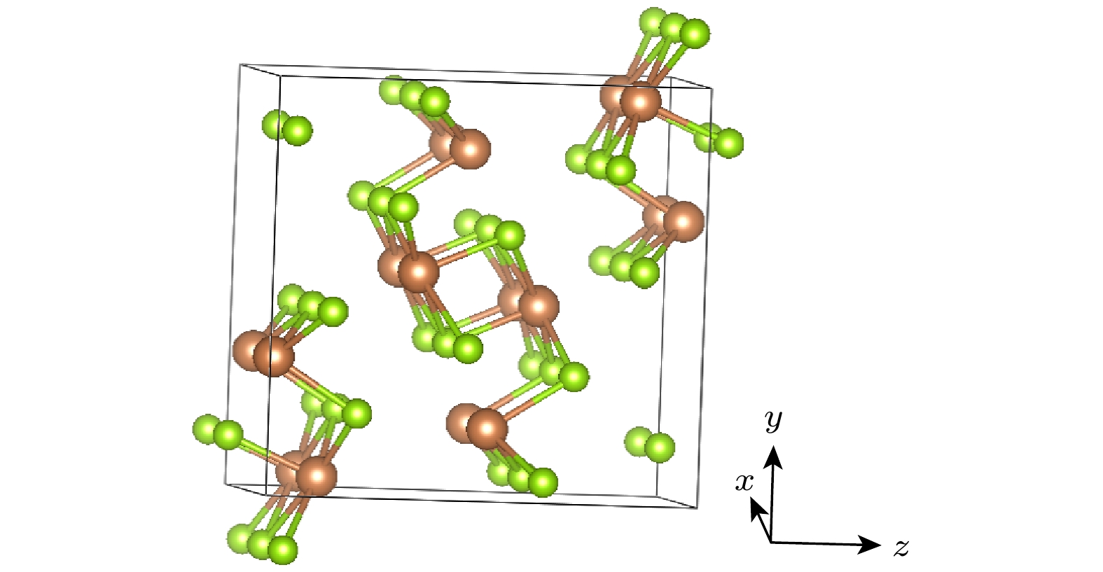
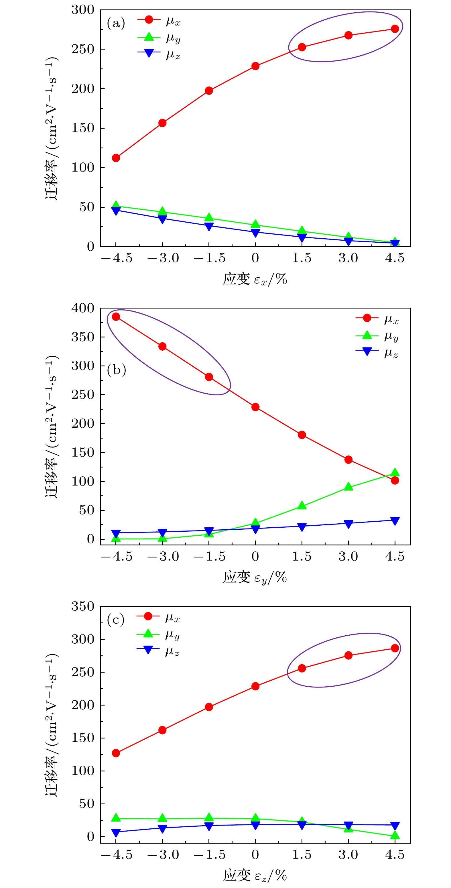
硒化锑(Sb2Se3)是一种物相简单、元素丰富、经济友好的太阳电池吸收层材料, 具有广阔的应用前景. 然而, Sb2Se3较弱的导电性成为了限制电池器件性能的重要因素. 迁移率是材料与器件的重要电学参数, 应变可以改变载流子迁移率, 因此, 研究应变对Sb2Se3的载流子迁移率特性影响具有实际意义. 本文通过密度泛函理论和形变势理论, 系统研究了单轴应变对Sb2Se3能带结构、禁带宽度、等能面、有效质量的影响, 分析了沿着x, y, z方向的三种单轴应变对载流子沿着x, y, z方向的迁移率μx, μy, μz的影响. 研究发现, 对于无应变的Sb2Se3, μx远大于μy和μz, 实验上应该将x方向作为Sb2Se3的特定生长方向(即内建电场方向). 综合应变对带隙、等能面、分态密度及迁移率的影响, 本研究认为当应变沿着y轴方向, 且压应变为3%的时候, 能获得最佳性能的Sb2Se3太阳电池吸收层材料.Antimony selenide (Sb2Se3) is a simple-phase, element-rich, and economically friendly material for solar cell absorption layers, with broad application prospects. However, the weak conductivity of Sb2Se3 has become a significant factor limiting the performance of solar cell devices. Carrier mobility is an important electrical parameter for both materials and devices, and strain can change carrier mobility. Therefore, studying the effect of strain on the carrier mobility of Sb2Se3 is of practical significance. In this work, using density functional theory and deformation potential theory, we systematically investigate the influence of uniaxial strain on the band structure, bandgap width, iso-surface, and effective mass of Sb2Se3. We analyze the effects of three types of uniaxial strains along the x-, y-, and z-direction on the carrier mobilities along the x-, y-, and z-direction, which are denoted by μx, μy, and μz, respectively. It is found that under these strains, the valence band maximum (VBM) position of Sb2Se3 remains unchanged, and the bandgap decreases with the increase of strain along the y- and z-direction, while it increases along the x-direction. The variation in bandgap may be related to the coupling strength between the Sb-5p orbital and Se-4p orbital of the conduction band minimum (CBM). For fully relaxed Sb2Se3, its iso-surface exhibits a distorted cylindrical shape, with low dispersion along the z-axis and high dispersion along the x- and y-axis, where μx is greater than μy and μz, suggesting that the x-direction should be considered as the specific growth direction for Sb2Se3 experimentally. When the strain is applied along the x- and z-direction, μx gradually increases with strain increasing, while it decreases when the strain is applied along the y-direction. Taking into account the combined effects of strain on bandgap, iso-surface, density of states, and mobility, this study suggests that the optimal performance of Sb2Se3 solar cell absorber layer material can be realized when the strain is applied along the y-axis, with a compressive strain of 3%.
-
Keywords:
- Sb2Se3 /
- mobility /
- deformation potential /
- strain engineering
[1] Green M A, Dunlop E D, Yoshita M 2023 Prog. Photovolt. Res. Appl. 31 651
 Google Scholar
[2] Chen C, Li K H, Tang J 2022 Sol. RRL 6 2200094
 Google Scholar
[3] Zhang X, Li C, Sun K, Zhou J, Zhang Z 2021 Adv. Energy Mater. 11 2002614
 Google Scholar
[4] 薛丁江, 石杭杰, 唐江 2015 64 038406
 Google Scholar
Xue D J, Shi H J, Tang J 2015 Acta Phys. Sin. 64 038406
 Google Scholar
[5] Zhao Y Q, Wang S Y, Li C, Che B, Chen X L, Chen H Y, Tang R F, Wang X M, Chen G L, Wang T, Gong J B, Chen T, Xiao X D, Li J M 2022 Energy Environ. Sci. 15 5118
 Google Scholar
[6] Li Z Q, Liang X Y, Li G, Liu H X, Zhang H Y, Guo J X, Chen J W, Shen K, San X Y, Yu W Y, Schropp R, Mai Y H 2019 Nat. Commun. 10 125
 Google Scholar
[7] Takagi S, Hoyt J L, Welser J J, Gibbons J F 1996 J. Appl. Phys. 80 1567
 Google Scholar
[8] Welser J, Hoyt J L, Gibbons J F 1992 International Technical Digest on Electron Devices Meeting, San Francisco, CA, USA 1992, December 13–16, 1992 p1000
[9] 宋建军, 张鹤鸣, 胡辉勇, 宣荣喜, 戴显英 2010 59 579
 Google Scholar
Song J J, Zhang H M, Hu H Y, Xuan R X, Dai X Y 2010 Acta Phys. Sin. 59 579
 Google Scholar
[10] Jia W L, He Y, Cao Y L, Wang X M, Lin Z, Li W T, Xu M, Li E L 2022 Micro Nanostructures 168 207300
 Google Scholar
[11] Datye I M, Daus A, Grady R W, Brenner K, Vaziri S, Pop E 2022 Nano Lett. 22 8052
 Google Scholar
[12] Ge G X, Zhang Y W, Yan H X, Yang J M, Zhou L, Sui X J 2021 Appl. Surf. Sci. 538 148009
 Google Scholar
[13] Perdew J P, Burke K, Ernzerhof M 1996 Phys. Rev. Lett. 77 3865
 Google Scholar
[14] Vadapoo R, Krishnan S, Yilmaz H, Marin C 2011 Phys. Status Solidi B 248 700
 Google Scholar
[15] Bardekn J, Shockley W 1950 Phys. Rev. 80 72
 Google Scholar
[16] Xi J Y, Long M Q, Tang L, Wang D, Shuai Z G 2012 Nanoscale 4 4348
 Google Scholar
[17] El-Sayad E A, Moustafa A M, Marzouk S Y 2009 Physica B 404 1119
 Google Scholar
[18] Kumar A, Ahluwalia P K 2013 Physica B 419 66
 Google Scholar
[19] Peng X H, Ganti S, Alizadeh A, Sharma P, Kumar S K, and Nayak S K 2006 Phys. Rev. B 74 035339
 Google Scholar
[20] Wang V, Xu N, Liu J C, Tang G, Geng W T 2021 Comput. Phys. Commun. 267 108033
 Google Scholar
[21] Kawamura M 2019 Comput. Phys. Commun. 239 197
 Google Scholar
[22] Wang X W, Li Z Z, Kavanagh S R, Ganose A M, Walsh A 2022 Phys. Chem. Chem. Phys. 24 7195
 Google Scholar
[23] Effective Mass Calculator for Semiconductors, Fonari A, Sutton Chttps://github.com/afonari/emc [2013-3-18]
[24] Zhang B Y, Qian X F 2022 ACS Appl. Energy Mater. 5 492
 Google Scholar
[25] Zhou Y, Wang L, Chen S Y, Qin S K, Liu X S, Chen Jie, Xue D J, Luo M, Cao Y Z, Cheng Y B, Sargent E H, Tang J 2015 Nat. Photonics 9 409
 Google Scholar
[26] Chen C, Bobela D C, Yang Ye, Lu S C, Zeng K, Ge C, Yang B, Gao L, Zhao Y, Beard M C, Tang J 2017 Front. Optoelectron. 10 18
 Google Scholar
-
图 4 Sb2Se3价带顶下100 meV处的等能面的变化. 应变沿着x方向上 (a) εx = 0, (b) εx = –4.5%, (c) εx = +4.5%; 应变沿y方向上 (d) εy = –4.5%, (e) εy = +4.5%; 应变沿z方向上 (f) εz = –4.5%, (g) εz = +4.5%
Fig. 4. Variation of the isosurface at 100 meV below VBM. The strain is applied along x direction: (a) εx = 0, (b) εx = –4.5%, and (c) εx = +4.5%. The strain is applied along y direction: (d) εy = –4.5% and (e) εy = +4.5%. The strain is applied along z direction: (f) εz = –4.5% and (g) εz = +4.5%.
图 5 Sb2Se3分态密度图. 应变沿着x方向上 (a) εx = 0, (b) εx = –4.5%, (c) εx = +4.5%; 应变沿y方向上 (d) εy = –4.5%, (e) εy = +4.5%; 应变沿z方向上 (f) εz = –4.5%, (g) εz = +4.5%
Fig. 5. Partial density of states of Sb2Se3. The strain is applied along x direction: (a) εx = 0, (b) εx = –4.5%, and (c) εx = +4.5%. The strain is applied along y direction: (d) εy = –4.5% and (e) εy = +4.5%. The strain is applied along z direction: (f) εz = –4.5% and (g) εz = +4.5%.
表 1 不同应变方向及应变量下, 沿x, y, z方向的有效质量
Table 1. Effective mass along x, y, z directions under different strain directions and strain amounts.
应变方向 ε/% $ {m}_{x}^{{\mathrm{*}}} $/m0 $ {m}_{y}^{{\mathrm{*}}} $/m0 $ {m}_{z}^{{\mathrm{*}}} $/m0
x方向–4.5 0.58 0.73 0.77 –3.0 0.51 0.78 0.86 –1.5 0.46 0.85 0.96 0 0.44 0.94 1.12 1.5 0.42 1.08 1.32 3.0 0.41 1.32 1.59 4.5 0.40 1.82 1.97
y方向–4.5 0.35 5.28 1.37 –3.0 0.37 4.24 1.29 –1.5 0.40 1.51 1.20 0 0.44 0.94 1.12 1.5 0.48 0.70 1.03 3.0 0.53 0.59 0.95 4.5 0.60 0.53 0.88
z方向–4.5 0.55 0.94 1.62 –3.0 0.50 0.94 1.27 –1.5 0.46 0.93 1.15 0 0.44 0.94 1.12 1.5 0.42 1.02 1.11 3.0 0.40 1.35 1.12 4.5 0.40 3.83 1.13 -
[1] Green M A, Dunlop E D, Yoshita M 2023 Prog. Photovolt. Res. Appl. 31 651
 Google Scholar
[2] Chen C, Li K H, Tang J 2022 Sol. RRL 6 2200094
 Google Scholar
[3] Zhang X, Li C, Sun K, Zhou J, Zhang Z 2021 Adv. Energy Mater. 11 2002614
 Google Scholar
[4] 薛丁江, 石杭杰, 唐江 2015 64 038406
 Google Scholar
Xue D J, Shi H J, Tang J 2015 Acta Phys. Sin. 64 038406
 Google Scholar
[5] Zhao Y Q, Wang S Y, Li C, Che B, Chen X L, Chen H Y, Tang R F, Wang X M, Chen G L, Wang T, Gong J B, Chen T, Xiao X D, Li J M 2022 Energy Environ. Sci. 15 5118
 Google Scholar
[6] Li Z Q, Liang X Y, Li G, Liu H X, Zhang H Y, Guo J X, Chen J W, Shen K, San X Y, Yu W Y, Schropp R, Mai Y H 2019 Nat. Commun. 10 125
 Google Scholar
[7] Takagi S, Hoyt J L, Welser J J, Gibbons J F 1996 J. Appl. Phys. 80 1567
 Google Scholar
[8] Welser J, Hoyt J L, Gibbons J F 1992 International Technical Digest on Electron Devices Meeting, San Francisco, CA, USA 1992, December 13–16, 1992 p1000
[9] 宋建军, 张鹤鸣, 胡辉勇, 宣荣喜, 戴显英 2010 59 579
 Google Scholar
Song J J, Zhang H M, Hu H Y, Xuan R X, Dai X Y 2010 Acta Phys. Sin. 59 579
 Google Scholar
[10] Jia W L, He Y, Cao Y L, Wang X M, Lin Z, Li W T, Xu M, Li E L 2022 Micro Nanostructures 168 207300
 Google Scholar
[11] Datye I M, Daus A, Grady R W, Brenner K, Vaziri S, Pop E 2022 Nano Lett. 22 8052
 Google Scholar
[12] Ge G X, Zhang Y W, Yan H X, Yang J M, Zhou L, Sui X J 2021 Appl. Surf. Sci. 538 148009
 Google Scholar
[13] Perdew J P, Burke K, Ernzerhof M 1996 Phys. Rev. Lett. 77 3865
 Google Scholar
[14] Vadapoo R, Krishnan S, Yilmaz H, Marin C 2011 Phys. Status Solidi B 248 700
 Google Scholar
[15] Bardekn J, Shockley W 1950 Phys. Rev. 80 72
 Google Scholar
[16] Xi J Y, Long M Q, Tang L, Wang D, Shuai Z G 2012 Nanoscale 4 4348
 Google Scholar
[17] El-Sayad E A, Moustafa A M, Marzouk S Y 2009 Physica B 404 1119
 Google Scholar
[18] Kumar A, Ahluwalia P K 2013 Physica B 419 66
 Google Scholar
[19] Peng X H, Ganti S, Alizadeh A, Sharma P, Kumar S K, and Nayak S K 2006 Phys. Rev. B 74 035339
 Google Scholar
[20] Wang V, Xu N, Liu J C, Tang G, Geng W T 2021 Comput. Phys. Commun. 267 108033
 Google Scholar
[21] Kawamura M 2019 Comput. Phys. Commun. 239 197
 Google Scholar
[22] Wang X W, Li Z Z, Kavanagh S R, Ganose A M, Walsh A 2022 Phys. Chem. Chem. Phys. 24 7195
 Google Scholar
[23] Effective Mass Calculator for Semiconductors, Fonari A, Sutton Chttps://github.com/afonari/emc [2013-3-18]
[24] Zhang B Y, Qian X F 2022 ACS Appl. Energy Mater. 5 492
 Google Scholar
[25] Zhou Y, Wang L, Chen S Y, Qin S K, Liu X S, Chen Jie, Xue D J, Luo M, Cao Y Z, Cheng Y B, Sargent E H, Tang J 2015 Nat. Photonics 9 409
 Google Scholar
[26] Chen C, Bobela D C, Yang Ye, Lu S C, Zeng K, Ge C, Yang B, Gao L, Zhao Y, Beard M C, Tang J 2017 Front. Optoelectron. 10 18
 Google Scholar
计量
- 文章访问数: 3889
- PDF下载量: 130
- 被引次数: 0


 下载:
下载:


