


-
容性耦合等离子体技术广泛应用在半导体工业、生物医药、环境等领域, 是不可替代的核心处理技术. 基于电非对称双频源驱动的容性耦合等离子体因其可以实现离子能量和离子通量的相对独立调控而一直被寄予厚望. 本文采用一维流体耦合蒙特卡罗模型和刻蚀槽模型, 对基于电非对称效应的双频容性耦合CF4/Ar混合气体放电进行了模拟研究. 研究表明, 随着电极间距的增大, 自偏压的绝对值和电负性均减小. 此外, 由于放电区域变大但边界损失保持不变, 会导致外部馈入功率显著增加和等离子体密度增大. 本文采用CF4/Ar混合气体, 其中Ar含量很高, 气体电负性不是很高, 因此放电模式在不同的电极间距下都是 α 模式和双极扩散模式的共同作用. 在电极间距逐渐变大的过程中, 因为自偏压的变化导致离子能量分布中最大离子能量减小并且离子能量展宽变窄, 功率极板处离子通量的变化不明显, 中性基团通量的增大十分显著, 这些变化最终导致相同时间内的刻蚀速率和形貌发生改变. 所以, 在未来研究中, 不仅离子能量和通量的独立控制, 优化离子通量和中性基团通量的协同作用达到调节刻蚀速率、改善刻蚀形貌同样是重要研究内容.
-
关键词:
- 电非对称效应 /
- 离子和中性基团的协同作用 /
- 电极间距 /
- 放电模式
The capacitive CF4/Ar discharges driven by a dual frequency source based on the electrical asymmetry effect (EAE) are studied by using a one-dimensional fluid coupled with Monte-Carlo (MC) model and a two-dimensional trench model. The effects, induced by varying the relative gap distance, on self-bias voltage, electronegativity, ion flux, neutral flux and other plasma characteristics are systematically discussed. In this asymmetric discharge, as the gap distance increases, the absolute value of the self-bias voltage and electronegativity decrease. Meanwhile, the plasma density and absorption power increase accordingly because the effective discharge area expands but the boundary loss is still limited. In addition, both$ \mathrm{\alpha } $ mode and drift-ambipolar (DA) mode can play their important roles in the discharges with different gap distances, though DA mode is weakened in large gap discharge. Owing to the fact that the self-bias is larger and electronegativity is stronger for the case of smaller gap distance, the sheath expansion electric field at the powered electrode and the bulk electric field heat the electrons, leading the ionization rate to greatly increase near the collapse of the sheath at the grounded electrode. Besides, at the larger gap distance, the maximum value of the ionization rate decreases due to the reduction of electrons with relatively high-energy, and the ionization rate near the grounded electrode is reduced evidently. Moreover, with the increase of the gap distance, the maximum ion energy decreases and the ion energy distribution width becomes smaller due to the reduction of the self-bias voltage. Meanwhile, the etching rate increases a lot since the neutral flux increases significantly near the powered electrode. However, as the gap distance increases to 5 cm, the etching rate stops increasing and the trench width at the bottom becomes narrow because the neutral flux increases greatly compared with ion flux, forming a thick layer of polymer. So, besides separately controlling the ion energy and flux, optimizing the synergistic effect of ion flux and neutral group flux to adjust the etching rate and improve the etching morphology is also an interesting topic in the asymmetric CF4/Ar discharges.-
Keywords:
- electrical asymmetry effect /
- the synergy of ions and neutrals /
- gap distance /
- discharge mode
[1] Makabe T, Petrović Z 2006 Plasma Electronics: Applications in Microelectronic Device Fabrication (London: Taylor and Francis) pp3−9
[2] Lieberman M A, Lichtenberg A J 2005 Principles of Plasma Discharges and Materials Processing (New York: Wiley) pp1−750
[3] Agarwal A, Kushner M J 2009 J. Vac. Sci. Technol. A 27 37
 Google Scholar
[4] Sherpa S D, Ranjan A 2016 J. Vac. Sci. Technol. A 35 01A102
Google Scholar
[5] Sekine M 2002 Appl. Surf. Sci. 192 270
Google Scholar
[6] Kanarik K J, Tan S, Gottscho R A 2018 J. Phys. Chem. Lett. 9 4814
Google Scholar
[7] Kanarik K J, Hudson E A, Gottscho R A, et al. 2015 J. Vac. Sci. Technol. A 33 020802
Google Scholar
[8] Huang S, Huard C, Shim S, Nam S K, Song I C, Lu S, Kushner M J 2019 J. Vac. Sci. Technol. A 37 031304
Google Scholar
[9] Takayoshi T, Hiroki K, HoriMasaru Z M, Akiko K, Toshihisa N, Nobuyoshi K 2016 J. Vac. Sci. Technol. A 35 01A103
Google Scholar
[10] Booth J P, Cunge G, Chabert P, Sadeghi N 1999 J. Appl. Phys. 85 3097
Google Scholar
[11] Williams K L, Martin I T, Fisher E R 2002 J. Am. Soc. MASS Spectrom. 13 518
Google Scholar
[12] Flamm D L, Herb G K 1989 WITHDRAWN: Plasma Etching Technology—An Overview (Pittsburgh: Academic Press) pp1−89
[13] Sankaran A, Kushner M J 2004 J. Vac. Sci. Technol. A 22 1260
Google Scholar
[14] Gasvoda R J, Van De Steeg A W, Bhowmick R, Hudson E A, Agarwal S 2017 ACS Appl. Mater. Interfaces 9 31067
Google Scholar
[15] Stoffels W W, Stoffels E, Tachibana K 1998 J. Vac. Sci. Technol. A 16 87
Google Scholar
[16] Cunge G, Booth J P 1999 J. Appl. Phys. 85 3952
Google Scholar
[17] Zhang D, Kushner M J 2000 J. Vac. Sci. Technol. A 18 2661
Google Scholar
[18] Metzler D, Engelmann S, Bruce R L, Oehrlein G S, Joseph E A, Li C 2015 J. Vac. Sci. Technol. A 34 01B101
Google Scholar
[19] Winters H F, J.W.Coburn 1992 Surf. Sci. Rep. 14 161
Google Scholar
[20] Sasaki K, Furukawa H, Suzuki C, Kadota K 1999 J. Appl. Phys. 38 954
Google Scholar
[21] Kimizuka M, Ozaki Y, Watanabe Y 1997 J. Vac. Sci. Technol. B 15 66
Google Scholar
[22] Capps N E, Mackie N M, Fisher E R 1998 J. Appl. Phys. 84 4736
Google Scholar
[23] Fendel P, Francis A, Czarnetzki U 2005 Plasma Sources Sci. Technol. 14 1
Google Scholar
[24] Booth J P, Abada H, Chabert P, Graves D B 2005 Plasma Sources Sci. Technol. 14 273
Google Scholar
[25] Kanarik K J, Tan S, Yang W, et al. 2017 J. Vac. Sci. Technol. A 35 05C302
Google Scholar
[26] Huard C M Sriraman S, Kanarik K J, Zhang Y, Kushner M J, Paterson A 2017 J. Vac. Sci. Technol. A 35 031306
Google Scholar
[27] Heil B G, Czarnetzki U, Brinkmann R P, Mussenbrock T 2008 J. Phys. D. Appl. Phys. 41 165202
Google Scholar
[28] Zhang Y, Kushner M J, Sriraman S, Marakhtanov A, Holland J, Paterson A 2015 J. Vac. Sci. Technol. A 33 031302
Google Scholar
[29] Zhang Y, Zafar A, Coumou D J, Shannon S C, Kushner M J 2015 J. Appl. Phys. 117 233302
Google Scholar
[30] Zhang Y R, Hu Y T, Gao F, Song Y H, Wang Y N 2018 Plasma Sources Sci. Technol. 27 55003
Google Scholar
[31] Zhang Y R, Hu Y T, Wang Y N 2020 Plasma Sources Sci. Technol. 29 84003
Google Scholar
[32] Schulze J, Derzsi A, Donkó Z 2011 Plasma Sources Sci. Technol. 20 045008
Google Scholar
[33] Brandt S, Berger B, Donkó Z, Derzsi A, Schüngel E, Koepke M, Schulze J 2019 Plasma Sources Sci. Technol. 28 95021
Google Scholar
[34] Wang X F, Jia W Z, Song Y H, Zhang Y Y, Dai Z L, Wang Y N 2017 Phys. Plasmas 24 113503
Google Scholar
[35] Phelps A V, Petrović Z L 1999 Plasma Sources Sci. Technol. 8 06B101
Google Scholar
[36] Tinck S, Boullart W, Bogaerts A 2009 J. Phys. D. Appl. Phys. 42 095204
Google Scholar
[37] Brandt S, Berger B, Schüngel E, et al. 2016 Plasma Sources Sci. Technol. 25 045015
Google Scholar
[38] Vasenkov A V, Li X, Oehrlein G S, Kushner M J 2004 J. Vac. Sci. Technol. A 22 511
Google Scholar
[39] Zhao S X, Gao F, Wang Y N, Bogaerts A 2012 Plasma Sources Sci. Technol. 21 025008
Google Scholar
[40] Huard C M, Sriraman S, Paterson A, Kushner M J 2018 J. Vac. Sci. Technol. A 36 06B101
Google Scholar
[41] Schulze J, Derzsi A, Dittmann K, Hemke T, Meichsner J, Donkó Z 2011 Phys. Rev. Lett. 107 275001
Google Scholar
-
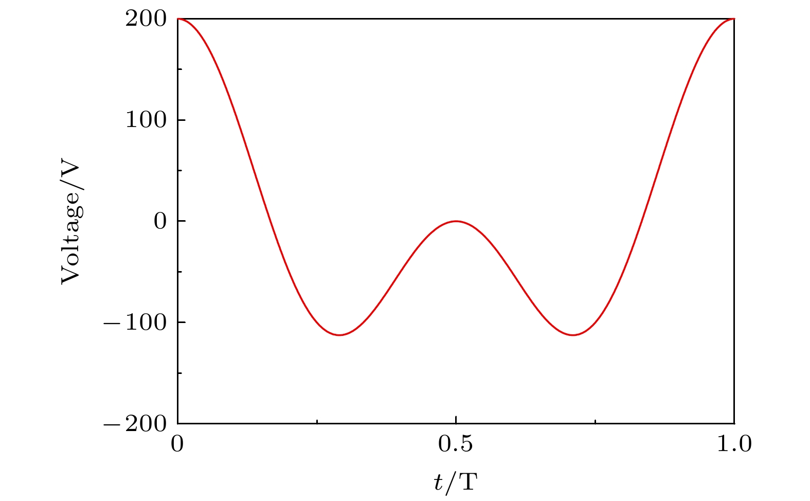
图 1 非对称双频电压波形图
Fig. 1. Asymmetrical dual-frequency voltage waveform used in this work.
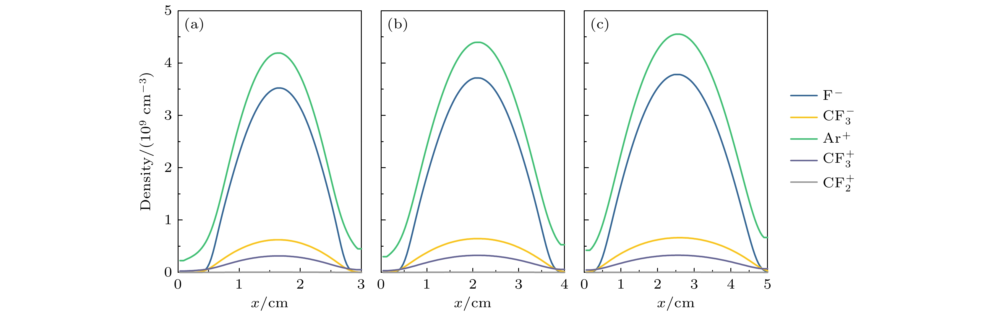
图 2 电极间距为(a) 3 cm, (b) 4 cm, (c) 5 cm下主要离子F–,
${\rm{CF}}_3^- $ , Ar+,${\rm{CF}}_3^+ $ ,${\rm{CF}}_2^+ $ 的周期平均密度Fig. 2. Period averaged densities of F–,
${\rm{CF}}_3^- $ , Ar+,${\rm{CF}}_3^+ $ , and${\rm{CF}}_2^+ $ for different gap distance of (a) 3 cm, (b) 4 cm, (c) 5 cm.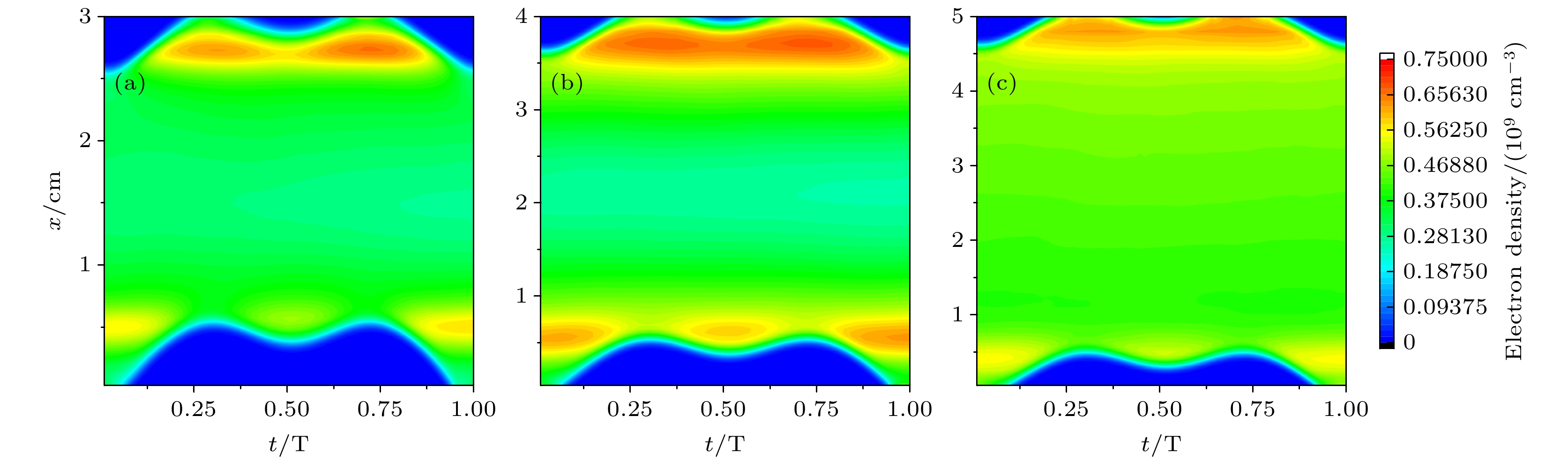
图 3 在不同电极间距(a) 3 cm, (b) 4 cm, (c) 5 cm下时空演化的电子密度
Fig. 3. Spatio-temporal evolution of electron density for different gap distance of (a) 3 cm, (b) 4 cm, (c) 5 cm.

图 4 不同电极间距下的自偏压以及时空平均的电负性
Fig. 4. Self-bias voltage and time-space averaged electronegativity for different gap distance.
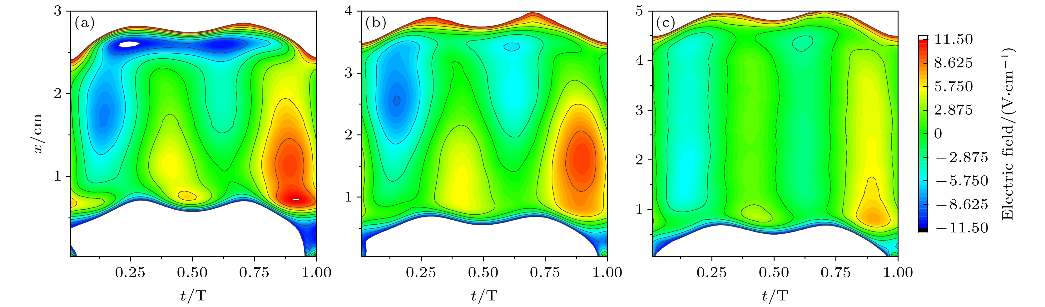
图 5 在不同电极间距下时空演化的电场 (a) 3 cm; (b) 4 cm; (c) 5 cm
Fig. 5. Spatio-temporal evolution of electric field for different gap distance of (a) 3 cm, (b) 4 cm, (c) 5 cm.

图 6 在不同电极间距下时空演化的电子功率吸收 (a) 3 cm; (b) 4 cm; (c) 5 cm
Fig. 6. Spatio-temporal evolution of electron power absorption rate for different gap distance of (a) 3 cm, (b) 4 cm, (c) 5 cm.
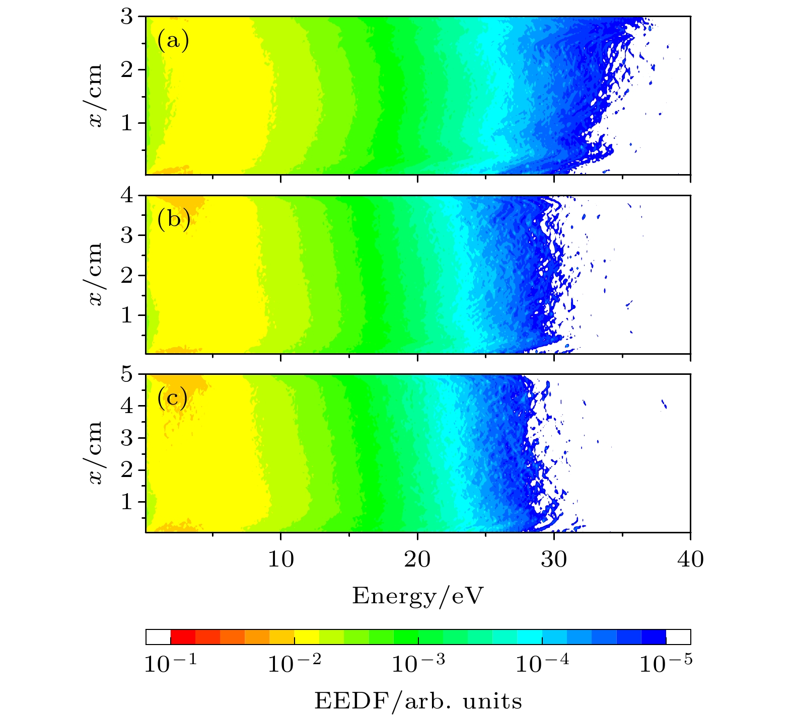
图 7 在不同电极间距下, 基频周期平均的电子能量分布函数(EEDF)的空间演化图 (a) 3 cm, (b) 4 cm, (c) 5 cm
Fig. 7. Time averaged EEDF for different gap distance of (a) 3 cm, (b) 4 cm, (c) 5 cm.

图 8 在不同电极间距下时空演化的电离率(Ar+e→Ar++2 e) (a) 3 cm; (b) 4 cm; (c) 5 cm
Fig. 8. Spatio-temporal evolution of ionization rate (Ar+e→Ar++2 e) for different gap distance of (a) 3 cm, (b) 4 cm, (c) 5 cm.
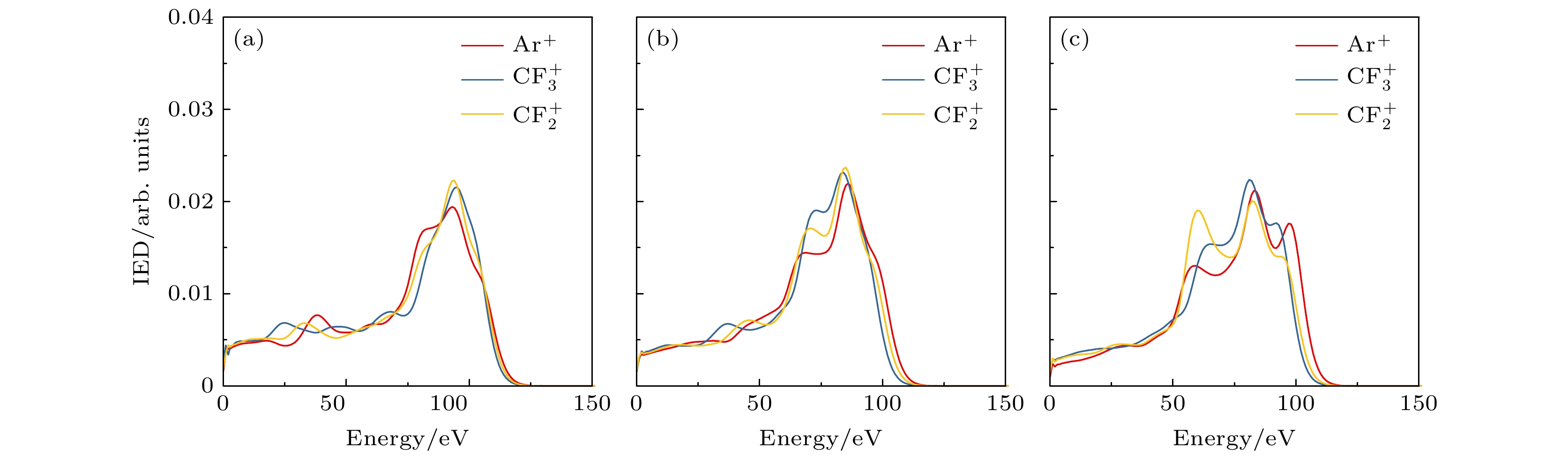
图 9 在电极间距为(a) 3 cm, (b) 4 cm, (c) 5 cm下功率电极处的离子能量分布函数.
Fig. 9. Ion energy distribution (IED) at the powered electrode for different gap distance of (a) 3 cm, (b) 4 cm, (c) 5 cm.
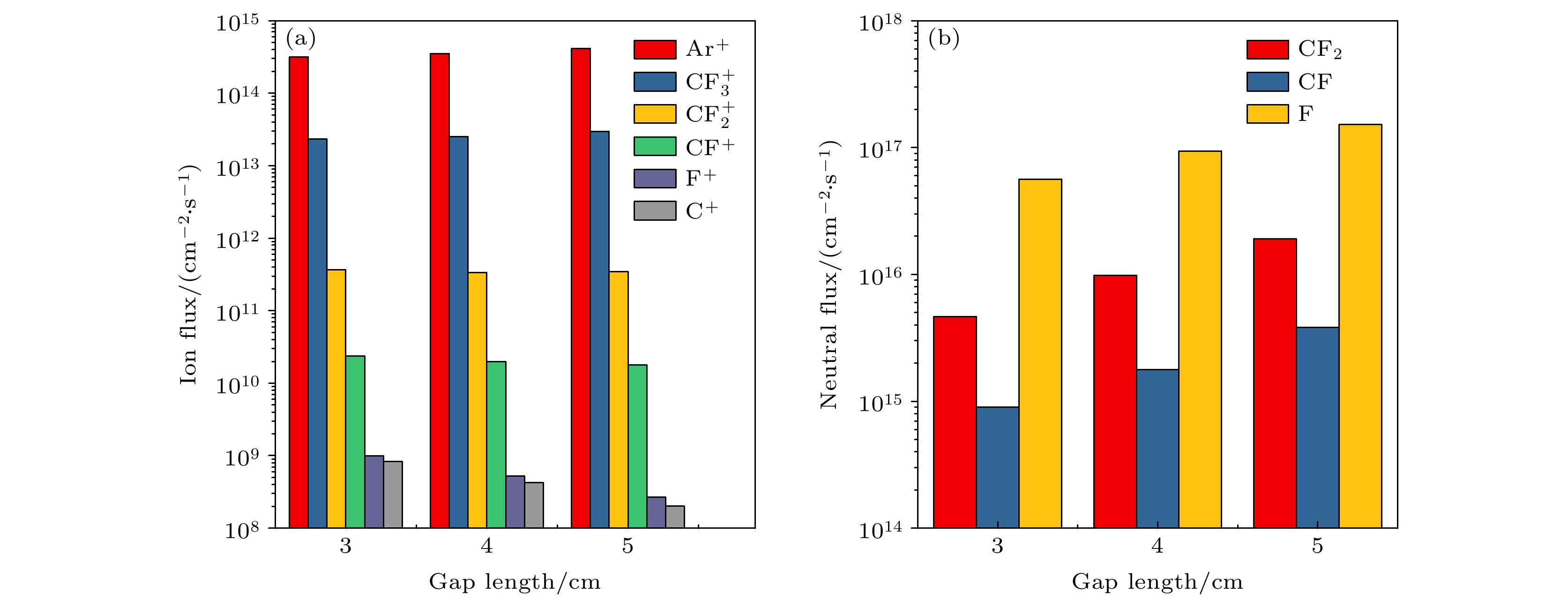
图 10 功率电极附近基频周期平均的(a)离子通量和(b)中性基团通量在不同电极间距下的变化情况
Fig. 10. (a) Ion flux and (b) neutral flux at the powered electrode for different gap distance.
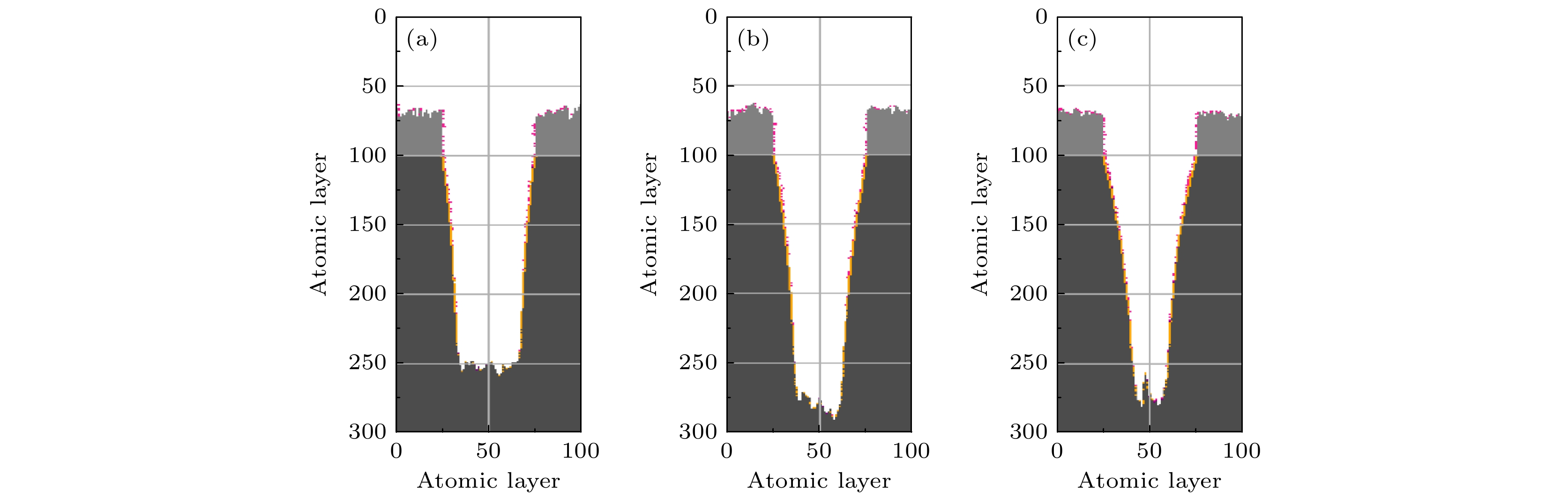
图 11 在电极间距为(a) 3 cm, (b) 4 cm, (c) 5 cm下刻蚀形貌
Fig. 11. Etching profiles for different gap distance of (a) 3 cm, (b) 4 cm, (c) 5 cm.
-
[1] Makabe T, Petrović Z 2006 Plasma Electronics: Applications in Microelectronic Device Fabrication (London: Taylor and Francis) pp3−9
[2] Lieberman M A, Lichtenberg A J 2005 Principles of Plasma Discharges and Materials Processing (New York: Wiley) pp1−750
[3] Agarwal A, Kushner M J 2009 J. Vac. Sci. Technol. A 27 37
Google Scholar
[4] Sherpa S D, Ranjan A 2016 J. Vac. Sci. Technol. A 35 01A102
Google Scholar
[5] Sekine M 2002 Appl. Surf. Sci. 192 270
Google Scholar
[6] Kanarik K J, Tan S, Gottscho R A 2018 J. Phys. Chem. Lett. 9 4814
Google Scholar
[7] Kanarik K J, Hudson E A, Gottscho R A, et al. 2015 J. Vac. Sci. Technol. A 33 020802
Google Scholar
[8] Huang S, Huard C, Shim S, Nam S K, Song I C, Lu S, Kushner M J 2019 J. Vac. Sci. Technol. A 37 031304
Google Scholar
[9] Takayoshi T, Hiroki K, HoriMasaru Z M, Akiko K, Toshihisa N, Nobuyoshi K 2016 J. Vac. Sci. Technol. A 35 01A103
Google Scholar
[10] Booth J P, Cunge G, Chabert P, Sadeghi N 1999 J. Appl. Phys. 85 3097
Google Scholar
[11] Williams K L, Martin I T, Fisher E R 2002 J. Am. Soc. MASS Spectrom. 13 518
Google Scholar
[12] Flamm D L, Herb G K 1989 WITHDRAWN: Plasma Etching Technology—An Overview (Pittsburgh: Academic Press) pp1−89
[13] Sankaran A, Kushner M J 2004 J. Vac. Sci. Technol. A 22 1260
Google Scholar
[14] Gasvoda R J, Van De Steeg A W, Bhowmick R, Hudson E A, Agarwal S 2017 ACS Appl. Mater. Interfaces 9 31067
Google Scholar
[15] Stoffels W W, Stoffels E, Tachibana K 1998 J. Vac. Sci. Technol. A 16 87
Google Scholar
[16] Cunge G, Booth J P 1999 J. Appl. Phys. 85 3952
Google Scholar
[17] Zhang D, Kushner M J 2000 J. Vac. Sci. Technol. A 18 2661
Google Scholar
[18] Metzler D, Engelmann S, Bruce R L, Oehrlein G S, Joseph E A, Li C 2015 J. Vac. Sci. Technol. A 34 01B101
Google Scholar
[19] Winters H F, J.W.Coburn 1992 Surf. Sci. Rep. 14 161
Google Scholar
[20] Sasaki K, Furukawa H, Suzuki C, Kadota K 1999 J. Appl. Phys. 38 954
Google Scholar
[21] Kimizuka M, Ozaki Y, Watanabe Y 1997 J. Vac. Sci. Technol. B 15 66
Google Scholar
[22] Capps N E, Mackie N M, Fisher E R 1998 J. Appl. Phys. 84 4736
Google Scholar
[23] Fendel P, Francis A, Czarnetzki U 2005 Plasma Sources Sci. Technol. 14 1
Google Scholar
[24] Booth J P, Abada H, Chabert P, Graves D B 2005 Plasma Sources Sci. Technol. 14 273
Google Scholar
[25] Kanarik K J, Tan S, Yang W, et al. 2017 J. Vac. Sci. Technol. A 35 05C302
Google Scholar
[26] Huard C M Sriraman S, Kanarik K J, Zhang Y, Kushner M J, Paterson A 2017 J. Vac. Sci. Technol. A 35 031306
Google Scholar
[27] Heil B G, Czarnetzki U, Brinkmann R P, Mussenbrock T 2008 J. Phys. D. Appl. Phys. 41 165202
Google Scholar
[28] Zhang Y, Kushner M J, Sriraman S, Marakhtanov A, Holland J, Paterson A 2015 J. Vac. Sci. Technol. A 33 031302
Google Scholar
[29] Zhang Y, Zafar A, Coumou D J, Shannon S C, Kushner M J 2015 J. Appl. Phys. 117 233302
Google Scholar
[30] Zhang Y R, Hu Y T, Gao F, Song Y H, Wang Y N 2018 Plasma Sources Sci. Technol. 27 55003
Google Scholar
[31] Zhang Y R, Hu Y T, Wang Y N 2020 Plasma Sources Sci. Technol. 29 84003
Google Scholar
[32] Schulze J, Derzsi A, Donkó Z 2011 Plasma Sources Sci. Technol. 20 045008
Google Scholar
[33] Brandt S, Berger B, Donkó Z, Derzsi A, Schüngel E, Koepke M, Schulze J 2019 Plasma Sources Sci. Technol. 28 95021
Google Scholar
[34] Wang X F, Jia W Z, Song Y H, Zhang Y Y, Dai Z L, Wang Y N 2017 Phys. Plasmas 24 113503
Google Scholar
[35] Phelps A V, Petrović Z L 1999 Plasma Sources Sci. Technol. 8 06B101
Google Scholar
[36] Tinck S, Boullart W, Bogaerts A 2009 J. Phys. D. Appl. Phys. 42 095204
Google Scholar
[37] Brandt S, Berger B, Schüngel E, et al. 2016 Plasma Sources Sci. Technol. 25 045015
Google Scholar
[38] Vasenkov A V, Li X, Oehrlein G S, Kushner M J 2004 J. Vac. Sci. Technol. A 22 511
Google Scholar
[39] Zhao S X, Gao F, Wang Y N, Bogaerts A 2012 Plasma Sources Sci. Technol. 21 025008
Google Scholar
[40] Huard C M, Sriraman S, Paterson A, Kushner M J 2018 J. Vac. Sci. Technol. A 36 06B101
Google Scholar
[41] Schulze J, Derzsi A, Dittmann K, Hemke T, Meichsner J, Donkó Z 2011 Phys. Rev. Lett. 107 275001
Google Scholar


 下载:
下载:


计量
- 文章访问数: 7979
- PDF下载量: 225
- 被引次数: 0
