-
采用一种绿色的等离子增强化学气相沉积法, 以Al2O3为衬底, Ga金属为镓源, N2为氮源, 在不采用催化剂的情况下, 成功制备获得了结晶质量良好的GaN纳米线. 研究表明, 生长温度可显著调控GaN纳米线的形貌, 当反应温度为950 ℃时, 生长出的GaN微米片为六边形; 当反应温度为1000 ℃时, 生长出了长度为10—20 μm的超长GaN纳米线. 随着反应时间增加, GaN纳米线的长度增加. GaN纳米线内部存在着压应力, 应力大小为0.84 GPa. 同时, 也进一步讨论了GaN纳米线无催化剂生长机制. GaN纳米线光致发光结果显示, GaN纳米线缺陷较少, 结晶质量良好, 在360 nm处有一个较为尖锐的本征发光峰, 可应用于紫外激光器等光电子器件. 本研究结果将为新型光电器件低成本绿色制备提供一个可行的技术方案.
-
关键词:
- GaN纳米线 /
- 等离子增强化学气相沉积 /
- 无催化剂 /
- 生长机理
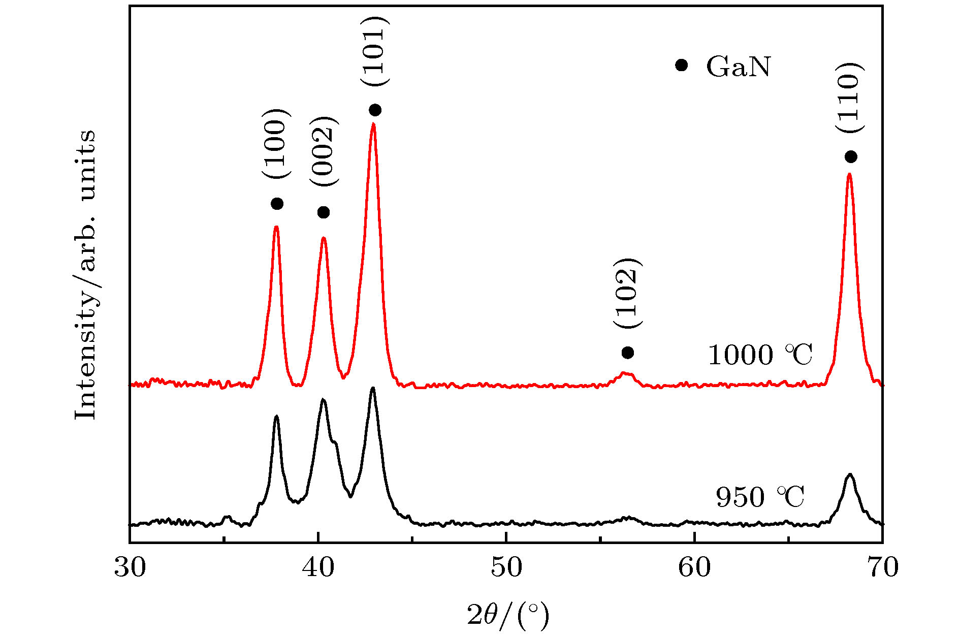
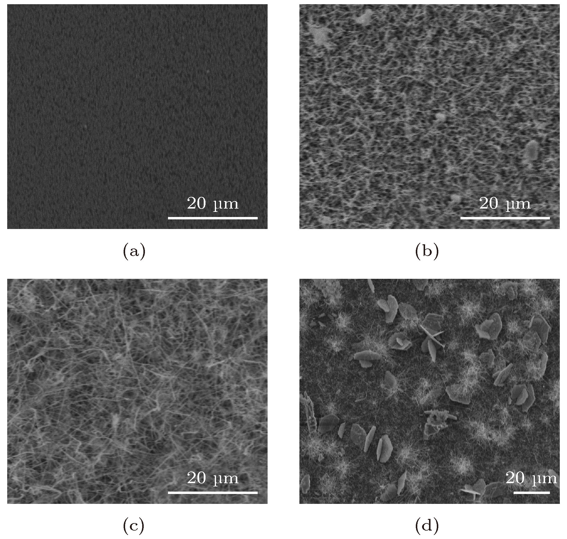
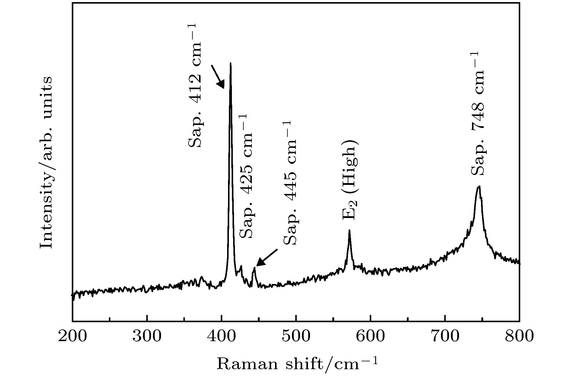
A green and low-cost method to prepare high-quality GaN (gallium nitride) nanowires is important for the applications of GaN-based devices on a large scale. In this work, high-quality GaN nanowires are successfully prepared by a green plasma enhanced chemical vapor deposition method without catalyst, with Al2O3 used as a substrate, metal Ga as a gallium source and N2 as a nitrogen source. The obtained GaN nanomaterials are investigated by using X-ray diffraction (XRD), scanning electron microscopy (SEM), transmission electron microscopy (TEM), Raman spectroscopy, and photoluminescence (PL) spectroscopy. The XRD results demonstrate that hexagonal-wurtzite GaN is obtained and no other phases exist. The SEM results show that GaN nanowires and hexagonal GaN microsheets are obtained at different temperatures. When the growth temperature is at 950 ℃ (reaction time for 2 h), the hexagonal GaN microsheets each with a size of 15 μm are obtained. When the growth temperature is at 1000 ℃(reaction time for 2 h), the GaN nanowires with the lengths in a range of 10–20 μm are obtained. With the reaction temperature increasing from 0.5 h to 2 h, the lengths of GaN nanowires increase. The TEM results suggest that the GaN nanowires are of high crystallinity and the growth direction of GaN nanowires is in the [0001] direction. The Raman results indicate that there exists a compressive stress in the GaN nanowires and its value is 0.84 GPa. Meanwhile, the growth mechanism of GaN nanowires is also proposed. The morphologies of GaN nanomaterials are tailed by the growth temperature, which may be caused by Ga atomic surface diffusion. Ga atoms have low diffusion energy and small diffusion length at 950 ℃. They gather in the non-polar m-plane. The (0001) plane with the lowest energy begins to grow. Then, hexagonal GaN microsheets are obtained. When reaction temperature is at 1000 ℃, the diffusion length of Ga atoms increases. Ga atoms can diffuse into (0001) plane. In order to maintain the lowest surface energy, the GaN nanowires grow along the [0001] direction. The PL results indicate that the obtained GaN nanowires have just an intrinsic and sharp luminescence peak at 360 nm, which possesses promising applications in photoelectric devices such as ultraviolet laser emitter. Our research will also provide a low-cost and green technical method of fabricating the new photoelectric devices.-
Keywords:
- GaN nanowires /
- plasma enhanced chemical vapor deposition /
- no catalyst /
- growth mechanism
[1] Lin Y, Yang M, Wang W, Lin Z, Li G 2016 Cryst. Eng. Comm. 18 8926
 Google Scholar
[2] Takekawa N, Hayashida N, Ohzeki D, Yamaguchi A, Murakami H, Kumagai Y, Matsumoto K, Koukitu A 2018 J. Cryst. Growth 502 7
 Google Scholar
[3] Wang X F, Zhang Y, Chen X M, He M, Liu C, Yin Y A, Zou X S, Li S T 2014 Nanoscale 6 12009
 Google Scholar
[4] Patsha A, Amirthapandian S, Pandian R, Dhara S 2013 J. Mater. Chem. C 1 8086
 Google Scholar
[5] 陈程程, 刘立英, 王如志, 宋雪梅, 王波, 严辉 2013 62 177701
 Google Scholar
Chen C C, Liu L Y, Wang R Z, Song X M, Wang B, Yan H 2013 Acta Phys. Sin. 62 177701
 Google Scholar
[6] Calarco R, Meijers R J, Debnath K R, Stoica T, Sutter E, Luth H 2007 Nano Lett. 7 2248
 Google Scholar
[7] Kumaresan V, Largeau L, Madouri A, Glas F, Zhang H Z, Oehler F, Cavanna A, Babichev A, Travers L, Gogneau N, Tchernycheva M, Harmand C J 2016 Nano Lett. 16 4895
 Google Scholar
[8] Kesaria M, Shetty S, Shivaprasad M S 2011 Cryst. Growth Des. 11 4900
 Google Scholar
[9] Kuykendall T, Pauzauskie P, Lee S K, Zhang Y F, Goldberger J, Yang P D 2003 Nano Lett. 3 1063
 Google Scholar
[10] Ji Y H, Wang R Z, Feng X Y, Zhang Y F, Yan H 2017 J. Phys. Chem. C 121 24804
 Google Scholar
[11] Wang Y Q, Wang R Z, Li Y J, Zhang Y F, Zhu M K., Wang B B, Yan H 2013 Cryst. Eng. Comm 15 1626
 Google Scholar
[12] Zhao J W, Zhang Y F, Li Y H, Su C H, Song X M, Yan H, Wang R Z 2015 Sci. Rep. 5 17692
 Google Scholar
[13] Jacobs B W, Crimp M A, McElroy K, Ayres V M 2008 Nano Lett. 8 4353
 Google Scholar
[14] Chang K W, Wu J J 2002 J. Phys. Chem. B 106 7796
 Google Scholar
[15] Stamplecoskie K G, Ju L, Farvid S S, Radovanovic P V 2008 Nano Lett. 8 2674
 Google Scholar
[16] Li C, Bando Y, Golberg D 2010 ACS Nano 4 2422
 Google Scholar
[17] 赵军伟, 张跃飞, 宋雪梅, 严辉, 王如志 2014 63 117702
 Google Scholar
Zhao J W, Zhang Y F, Song X M, Yan H, Wang R Z 2014 Acta Phys. Sin. 63 117702
 Google Scholar
[18] Schiaber Z D, Calabrese G, Kong X, Trampert A, Jenichen B, de Silva J HD, Geelhaar L, Brandt O, Fermandez-Garrido S 2017 Nano Lett. 17 63
 Google Scholar
[19] Choi S, Song H G, Yoo Y S, Lee C, Woo K Y, Lee E, Roh S D, Cho Y H 2018 ACS Photonics 5 2825
 Google Scholar
[20] Feng X Y, Wang R Z, Liang Q, Ji Y H, Yang M Q 2019 Cryst. Growth Des. 19 2687
 Google Scholar
[21] Wei X F, Shi F 2011 Appl. Surf. Sci. 257 9931
 Google Scholar
[22] Shen L H, Cheng T M, Wu L J, Li X G, Cui Q L 2008 J. Alloys Compd. 465 562
 Google Scholar
[23] Ramesh C, Tyagi P, Bhattacharyya B, Husale S, Maurya K K, Kumar M S, Kushvaha S S 2019 J. Alloys Compd. 770 572
 Google Scholar
[24] Purushothaman V, Ramakrishnan V, Jeganathan K 2012 Cryst. Eng. Comm. 14 8390
 Google Scholar
[25] Purushothaman V, Ramakrishnan V, Jeganathan K 2012 RSC Adv. 2 4802
 Google Scholar
[26] Li Y, Wang W L, Li X C, Huang L G, Lin Z T, Zheng Y L, Chen X F, Li G Q 2019 J. Alloys Compd. 771 1000
 Google Scholar
[27] Wei P C, Chen L C, Chen K H 2014 J. Appl. Phys. 116 124301
 Google Scholar
[28] Wu C, Yu J D, E Y X, Luo Y, Hao Z B, Wang J, Wang L, Sun C Z, Xiong B, Han Y J, Li H T 2016 Cryst. Growth Des. 16 5023
 Google Scholar
[29] Xian Y L, Huang S J, Zheng Z Y, Fan B F, Wu Z S, Jiang H, Wang G 2011 J. Cryst. Growth 325 32
 Google Scholar
[30] Matoussi A, Nasr F B, Boufaden T, Salh R, Fakhfakh Z, Guermazi S, ElJani B, Fitting H J 2010 J. Lumin. 130 399
 Google Scholar
[31] Sun R, Wang G G, Peng Z C 2018 Mater. Lett. 217 288
 Google Scholar
-
图 3 1000 ℃反应2 h获得GaN纳米线的TEM图 (a) 单根GaN纳米线的TEM照片; (b) 图(a)中的GaN纳米线的高倍TEM照片; (c) 另一根GaN纳米线的TEM照片; (d) 图(c)中的GaN纳米线的高倍TEM照片
Fig. 3. TEM images of GaN nanowires fabricated at 1000 ℃ (Reaction time is 2 h): (a) TEM image of single GaN nanowire; (b) HR-TEM image of GaN nanowire in (a); (c) TEM image of another GaN nanowire; (d) HR-TEM image of GaN nanowire in (c).
-
[1] Lin Y, Yang M, Wang W, Lin Z, Li G 2016 Cryst. Eng. Comm. 18 8926
 Google Scholar
[2] Takekawa N, Hayashida N, Ohzeki D, Yamaguchi A, Murakami H, Kumagai Y, Matsumoto K, Koukitu A 2018 J. Cryst. Growth 502 7
 Google Scholar
[3] Wang X F, Zhang Y, Chen X M, He M, Liu C, Yin Y A, Zou X S, Li S T 2014 Nanoscale 6 12009
 Google Scholar
[4] Patsha A, Amirthapandian S, Pandian R, Dhara S 2013 J. Mater. Chem. C 1 8086
 Google Scholar
[5] 陈程程, 刘立英, 王如志, 宋雪梅, 王波, 严辉 2013 62 177701
 Google Scholar
Chen C C, Liu L Y, Wang R Z, Song X M, Wang B, Yan H 2013 Acta Phys. Sin. 62 177701
 Google Scholar
[6] Calarco R, Meijers R J, Debnath K R, Stoica T, Sutter E, Luth H 2007 Nano Lett. 7 2248
 Google Scholar
[7] Kumaresan V, Largeau L, Madouri A, Glas F, Zhang H Z, Oehler F, Cavanna A, Babichev A, Travers L, Gogneau N, Tchernycheva M, Harmand C J 2016 Nano Lett. 16 4895
 Google Scholar
[8] Kesaria M, Shetty S, Shivaprasad M S 2011 Cryst. Growth Des. 11 4900
 Google Scholar
[9] Kuykendall T, Pauzauskie P, Lee S K, Zhang Y F, Goldberger J, Yang P D 2003 Nano Lett. 3 1063
 Google Scholar
[10] Ji Y H, Wang R Z, Feng X Y, Zhang Y F, Yan H 2017 J. Phys. Chem. C 121 24804
 Google Scholar
[11] Wang Y Q, Wang R Z, Li Y J, Zhang Y F, Zhu M K., Wang B B, Yan H 2013 Cryst. Eng. Comm 15 1626
 Google Scholar
[12] Zhao J W, Zhang Y F, Li Y H, Su C H, Song X M, Yan H, Wang R Z 2015 Sci. Rep. 5 17692
 Google Scholar
[13] Jacobs B W, Crimp M A, McElroy K, Ayres V M 2008 Nano Lett. 8 4353
 Google Scholar
[14] Chang K W, Wu J J 2002 J. Phys. Chem. B 106 7796
 Google Scholar
[15] Stamplecoskie K G, Ju L, Farvid S S, Radovanovic P V 2008 Nano Lett. 8 2674
 Google Scholar
[16] Li C, Bando Y, Golberg D 2010 ACS Nano 4 2422
 Google Scholar
[17] 赵军伟, 张跃飞, 宋雪梅, 严辉, 王如志 2014 63 117702
 Google Scholar
Zhao J W, Zhang Y F, Song X M, Yan H, Wang R Z 2014 Acta Phys. Sin. 63 117702
 Google Scholar
[18] Schiaber Z D, Calabrese G, Kong X, Trampert A, Jenichen B, de Silva J HD, Geelhaar L, Brandt O, Fermandez-Garrido S 2017 Nano Lett. 17 63
 Google Scholar
[19] Choi S, Song H G, Yoo Y S, Lee C, Woo K Y, Lee E, Roh S D, Cho Y H 2018 ACS Photonics 5 2825
 Google Scholar
[20] Feng X Y, Wang R Z, Liang Q, Ji Y H, Yang M Q 2019 Cryst. Growth Des. 19 2687
 Google Scholar
[21] Wei X F, Shi F 2011 Appl. Surf. Sci. 257 9931
 Google Scholar
[22] Shen L H, Cheng T M, Wu L J, Li X G, Cui Q L 2008 J. Alloys Compd. 465 562
 Google Scholar
[23] Ramesh C, Tyagi P, Bhattacharyya B, Husale S, Maurya K K, Kumar M S, Kushvaha S S 2019 J. Alloys Compd. 770 572
 Google Scholar
[24] Purushothaman V, Ramakrishnan V, Jeganathan K 2012 Cryst. Eng. Comm. 14 8390
 Google Scholar
[25] Purushothaman V, Ramakrishnan V, Jeganathan K 2012 RSC Adv. 2 4802
 Google Scholar
[26] Li Y, Wang W L, Li X C, Huang L G, Lin Z T, Zheng Y L, Chen X F, Li G Q 2019 J. Alloys Compd. 771 1000
 Google Scholar
[27] Wei P C, Chen L C, Chen K H 2014 J. Appl. Phys. 116 124301
 Google Scholar
[28] Wu C, Yu J D, E Y X, Luo Y, Hao Z B, Wang J, Wang L, Sun C Z, Xiong B, Han Y J, Li H T 2016 Cryst. Growth Des. 16 5023
 Google Scholar
[29] Xian Y L, Huang S J, Zheng Z Y, Fan B F, Wu Z S, Jiang H, Wang G 2011 J. Cryst. Growth 325 32
 Google Scholar
[30] Matoussi A, Nasr F B, Boufaden T, Salh R, Fakhfakh Z, Guermazi S, ElJani B, Fitting H J 2010 J. Lumin. 130 399
 Google Scholar
[31] Sun R, Wang G G, Peng Z C 2018 Mater. Lett. 217 288
 Google Scholar
计量
- 文章访问数: 10768
- PDF下载量: 147
- 被引次数: 0


 下载:
下载:


