


-
通过以大晶粒水热ZnO薄膜作为发光层并加以恰当图案化处理的策略, 显著抑制了基于ZnO薄膜的金属-绝缘体-半导体(MIS)结构发光器件的电抽运随机激射的随机性. 采用激光直写光刻工艺, 先将硅衬底上的晶粒大小超过500 nm的水热ZnO薄膜图案化为大量的小方块(Block)和“街道(Street)”, 然后制备基于上述图案化ZnO薄膜的MIS结构(Au/SiO2/ZnO)发光器件(light-emitting device, LED). 研究表明: 在相同的注入电流下, 基于图案化ZnO薄膜的发光器件比基于未图案化ZnO薄膜的发光器件具有更少的随机激射模式; 且前者随Block边长的减小而具更少的激射模式, 同时其最强激射模式的波长在更窄的范围内波动. 值得指出的是: 在适当的条件(小注入电流和小Block边长)下, 基于图案化水热ZnO薄膜的发光器件还可产生单模随机激射. 此外, 对比研究还表明: 基于大晶粒水热ZnO薄膜的LED比基于小晶粒溅射ZnO薄膜的LED具有更小的激射阈值电流, 且在同样的注入电流下具有更少的激射模式和更高的激射光功率. 关于上述结果背后的物理机制, 分析指出: 对基于图案化ZnO薄膜的发光器件而言, 一方面由于单个Block内ZnO薄膜中的晶粒和晶界数量有限, 光多重散射被严重削弱, 那些能够通过光多重散射获得净光增益而产生随机激射的路径与ZnO薄膜未经图案化处理的情形相比要少得多. 另一方面, 由于单个Block空间有限, 不同激射模式之间的增益竞争使得空间上重叠较大的激射模式不能同时存在. 由于上述两方面的原因, 随着Block边长的减小, 发光器件随机激射的模式会变得更少. 此外, Block之间的光学耦合效应会加剧单个Block内部激射模式之间的增益竞争, 从而进一步减少发光器件的随机激射模式.In this work, the randomness of electrically pumped random laser (RL) from ZnO-based metal-insulator-semiconductor (MIS) structured light-emitting device (LED) is significantly suppressed, by using appropriately patterned hydrothermal ZnO film with large crystal grains as the light-emitting layer. The hydrothermal ZnO film on silicon substrate, with the crystal grains sized over 500 nm, is first patterned into a number of square blocks separated by streets by using laser direct writing photolithography. Based on such a patterned ZnO film, the MIS (Au/SiO2/ZnO) structured LEDs are prepared on silicon substrates. Under the same injection current, the LED with the patterned ZnO film exhibits much fewer RL modes than that with the non-patterned ZnO film and, moreover, the former displays ever-fewer RL modes with the the decrease of block size. Besides, the wavelength of the strongest RL mode from the LED with the patterned ZnO film fluctuates in a much narrower range than that with the non-patterned ZnO film. It is worth mentioning that the LED with the patterned hydrothermal ZnO film can even be pumped into the single-mode RL under the desirable conditions such as low injection current and small patterned blocks. Moreover, the comparative investigation indicates that the LED with the large-grain hydrothermal ZnO film exhibits the smaller RL threshold current than that with the small-grain sputtered ZnO film, and the former has fewer RL modes and a higher output lasing power than the latter under the same injection current. As for the physical mechanism behind the aforementioned results, it is analyzed as follows. Regarding the LED with the patterned ZnO film, on the one hand, due to the limited numbers of crystal grains and grain boundaries within a single block, the multiple optical scattering is remarkably suppressed. Then, the paths through which the net optical gain and therefore the lasing action can be achieved via multiple optical scattering are much fewer than those in the case of the non-patterned ZnO film. On the other hand, due to optical gain competition among different RL modes occurring within the limited space of a single block, the RL modes with significant spatial overlap cannot lase simultaneously. For the two-fold reasons as mentioned above, the LED exhibits ever-fewer RL modes with the decrease of the size of blocks. Moreover, the inter-block optical coupling enables the optical gain competition among different RL modes to be more violent within a single block, leading to further reduction of RL modes.
-
Keywords:
- hydrothermal ZnO film /
- light-emitting device /
- random lasing /
- patterning /
- suppression of randomness
[1] Cao H, Zhao Y G, Ong H C, Ho S T, Dai J Y, Wu J Y, Chang R P H 1998 Appl. Phys. Lett. 73 3656
 Google Scholar
[2] Yu S F, Leong E S P 2004 IEEE J. Quantum Electron. 40 1186
Google Scholar
[3] Cao H, Zhao Y G, Ong H C, Chang R P H 1999 Phys. Rev. B 59 15107
Google Scholar
[4] Thareja R K, Mitra A 2000 Appl. Phys. B: Lasers Opt. 71 181
Google Scholar
[5] Lau S P, Yang H Y, Yu S F, Li H D, Tanemura M, Okita T, Hatano H, Hng H H 2005 Appl. Phys. Lett. 87 013104
Google Scholar
[6] Ursaki V V, Burlacu A, Rusu E V, Postolake V, Tiginyanu I M 2009 J. Opt. A: Pure Appl. Opt. 11 075001
Google Scholar
[7] Yu S F, Yuen C, Lau S P, Park W I, Yi G C 2004 Appl. Phys. Lett. 84 3241
Google Scholar
[8] Ma X Y, Chen P L, Li D S, Zhang Y Y, Yang D R 2007 Appl. Phys. Lett. 91 251109
Google Scholar
[9] Chu S, Olmedo M, Yang Z, Kong J Y, Liu J L 2008 Appl. Phys. Lett. 93 181106
Google Scholar
[10] Long H, Fang G J, Huang H H, Mo X M, Xia W, Dong B Z, Meng X Q, Zhao X Z 2009 Appl. Phys. Lett. 95 013509
Google Scholar
[11] Zhu H, Shan C X, Zhang J Y, Zhang Z Z, Li B H, Zhao D X, Yao B, Shen D Z, Fan X W, Tang Z K, Hou X H, Choy K L 2010 Adv. Mater. 22 1877
Google Scholar
[12] Chen P L, Ma X Y, Li D S, Zhang Y Y, Yang D R 2009 Opt. Express 17 4712
Google Scholar
[13] Wang C X, Jiang H T, Li Y P, Ma X Y, Yang D R 2013 J. Appl. Phys. 114 133105
Google Scholar
[14] Wang C X, Zhu C, Lü C Y, Li D S, Ma X Y, Yang D R 2015 Appl. Surf. Sci. 332 620
Google Scholar
[15] Jiang S M, Xia C T, Ji R, Pang H W, Li D S, Yang D R, Ma X Y 2024 Acs Appl. Mater. Interfaces 16 3719
Google Scholar
[16] Ma X Y, Pan J W, Chen P L, Li D S, Zhang H, Yang Y, Yang D R 2009 Opt. Express 17 14426
Google Scholar
[17] Ryglowski L, Cyprych K, Mysliwiec J 2022 Opt. Commun. 510 127939
Google Scholar
[18] Li Y P, Wang C X, Jin L, Ma X Y, Yang D R 2013 Appl. Phys. Lett. 102 161112
Google Scholar
[19] 徐韵, 李云鹏, 金璐, 马向阳, 杨德仁 2013 62 084207
Google Scholar
Xu Y, Li Y P, Jin L, Ma X Y, Yang D R 2013 Acta Phys. Sin. 62 084207
Google Scholar
[20] Jiang X Y, Soukoulis C M 2000 Phys. Rev. Lett. 85 70
Google Scholar
[21] Sebbah P, Vanneste C 2002 Phys. Rev. B 66 144202
Google Scholar
[22] 杜文博, 冷进勇, 朱家健, 周朴, 许晓军, 舒柏宏 2012 61 114203
Google Scholar
Du W B, Leng J Y, Zhu J J, Zhou P, Xu X J, Shu B H 2012 Acta Phys. Sin. 61 114203
Google Scholar
[23] Zhu G Y, Tian M F, Almokhtar M, Qin F F, Li B H, Zhou M Y, Gao F, Yang Y, Ji X, He S Q, Wang Y J 2022 Chin. Phys. Lett. 39 123401 (in Chinese)
Google Scholar
[24] Liu H, Li S J, You Y Q, Wang J W, Sun J, Zhang L, Xiong L L 2023 Optik 281 170853
Google Scholar
[25] Wang Y Y, Xu C X, Jiang M M, Li J T, Dai J, Lu J F, Li P L 2016 Nanoscale 8 16631
Google Scholar
[26] 魏伟华, 李木天, 刘墨南 2018 67 064203
Google Scholar
Wei W H, Li M T, Liu M N 2018 Acta Phys. Sin. 67 064203
Google Scholar
[27] 马光辉, 张家斌, 张贺, 金亮, 王灌鑫, 徐英添 2019 中国光学 12 649
Google Scholar
Ma G H, Zhang J B, Zhang H, Jin L, Wang G X, Xu Y T 2019 Chin. Opt. 12 649
Google Scholar
-
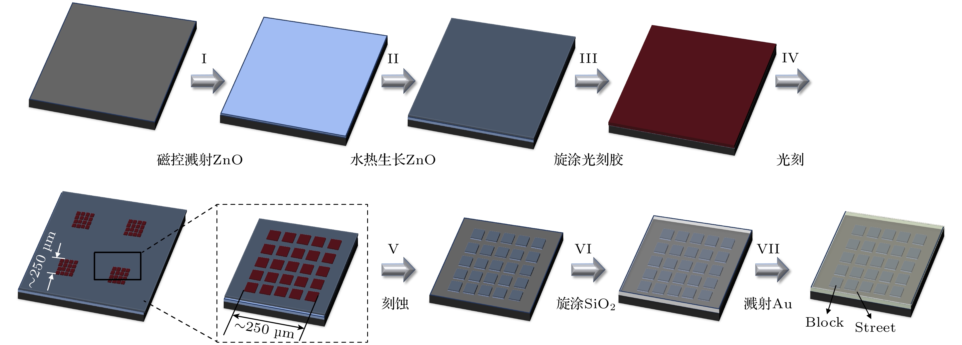
图 1 在硅衬底上制备基于图案化水热ZnO薄膜的MIS结构LED的步骤示意图
Fig. 1. Schematic diagram for the procedures of preparing MIS structured LEDs based on the patterned hydrothermal ZnO film on a silicon substrate.
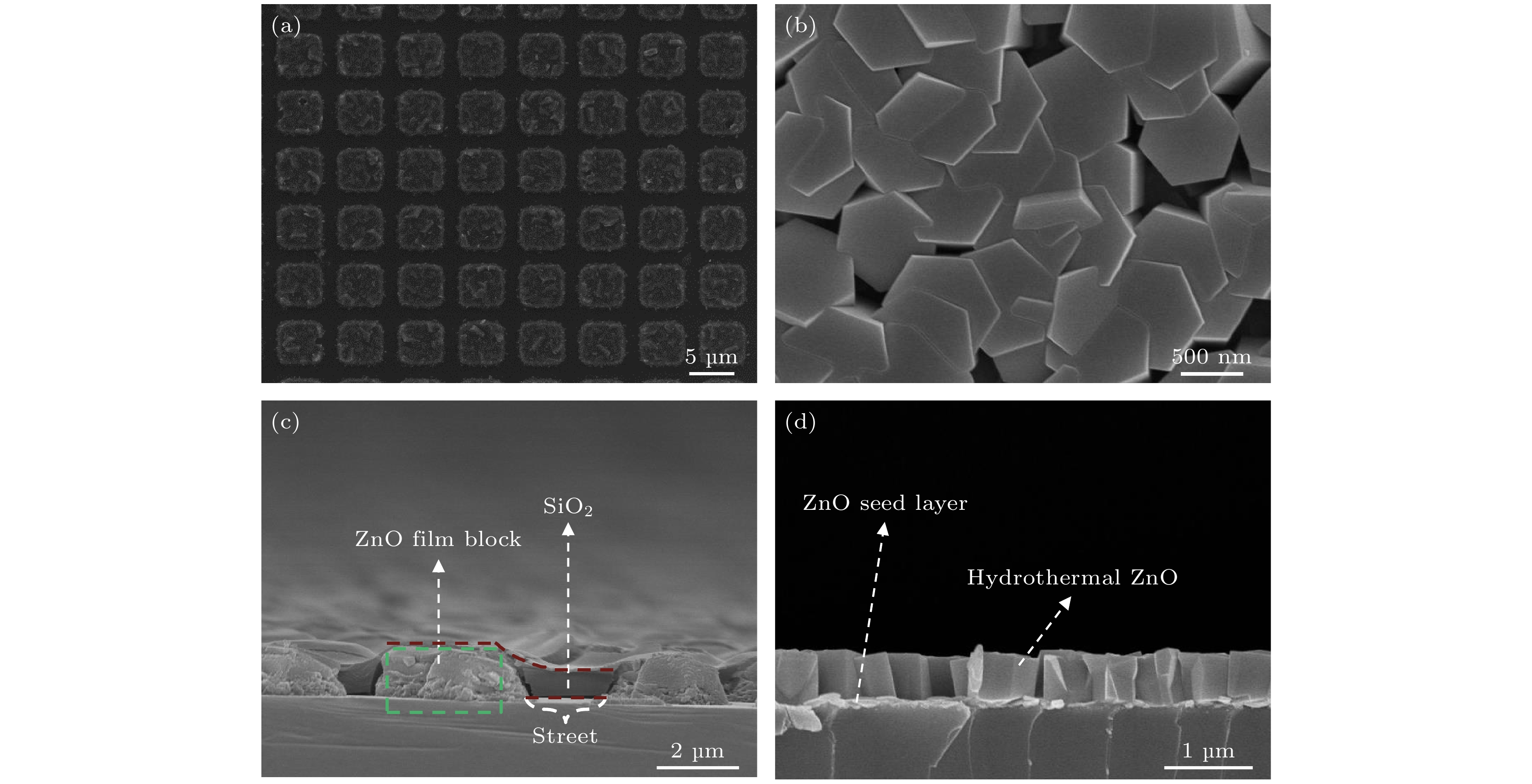
图 2 (a) 水热ZnO薄膜经图案化处理后的表面形貌SEM照片; (b) 单个Block内ZnO薄膜表面形貌的SEM照片; (c) Block和Street的截面SEM照片; (d) 单个Block的截面SEM照片
Fig. 2. (a) SEM image for the surface morphology of the patterned hydrothermal ZnO film; (b) SEM image for the surface morphology of the ZnO film within a single block; (c) cross-sectional SEM image for the blocks and streets; (d) cross-sectional SEM image for the ZnO film within a single block.
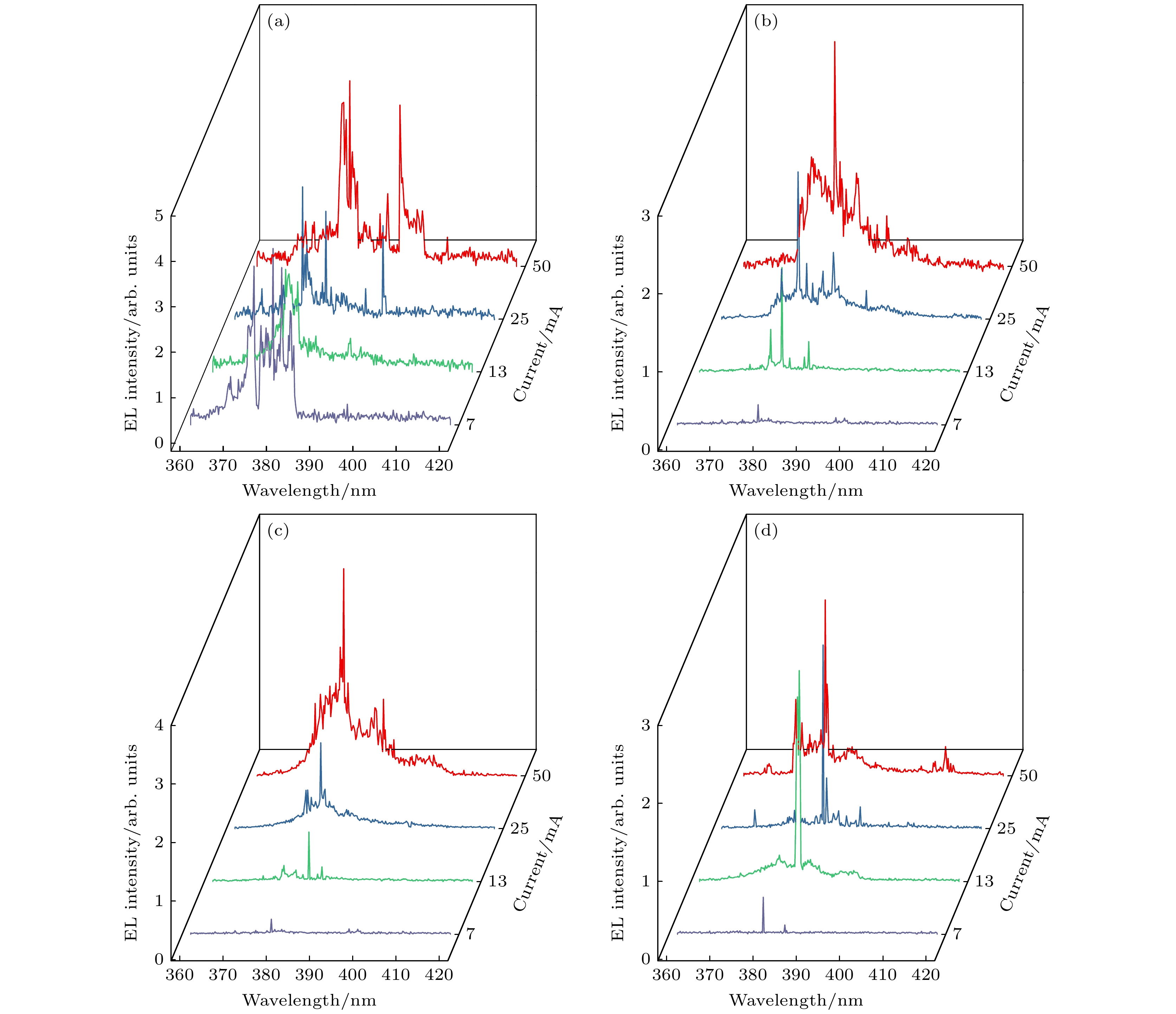
图 3 各种LED在不同注入电流下采集的电致发光谱 (a) 未经图案化处理的LED; (b) LED-10; (c) LED-5; (d) LED-2.5
Fig. 3. EL spectra acquired at different injection currents for various LEDs: (a) Non-patterned LED; (b) LED-10; (c) LED-5; (d) LED-2.5.
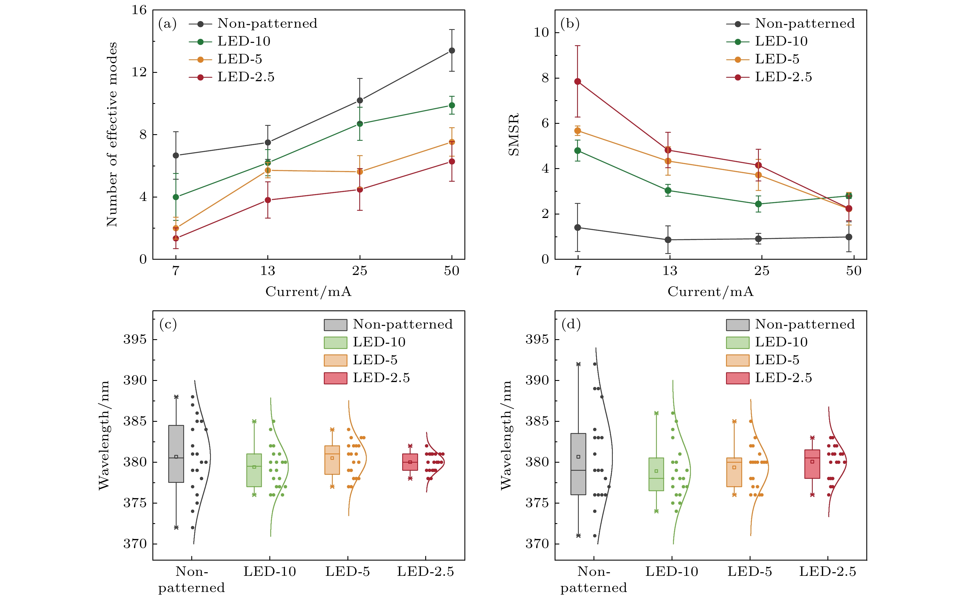
图 4 未经图案化处理的LED, LED-10, LED-5, LED-2.5的电抽运随机激射 (a), (b) 有效激射模式数和SMSR随注入电流的变化情况; (c), (d) 在注入电流分别为 7 mA和 25 mA时采集的20幅EL谱中最强激射峰的波长分布情况, 其中误差棒的最高点和最低点分别代表最大值和最小值, 方框的中间线代表中值、上边线和下边线分别代表第三四分位数和第一四分位数
Fig. 4. Electrically pumped random lasing from non-patterned LED, LED-10, LED-5, and LED-2.5: (a), (b) Number of effective lasing modes and SMSR as a function of injected current; (c), (d) distributions of the wavelengths of the strongest lasing peaks in the 20 EL spectra acquired at the injection currents of 7 mA and 25 mA, respectively, the error bar represents the minimum and maximum values, and the middle line in the box represents the median value, the upper and lower lines of the box represent the third quartile (Q3) and first quartile (Q1), respectively.
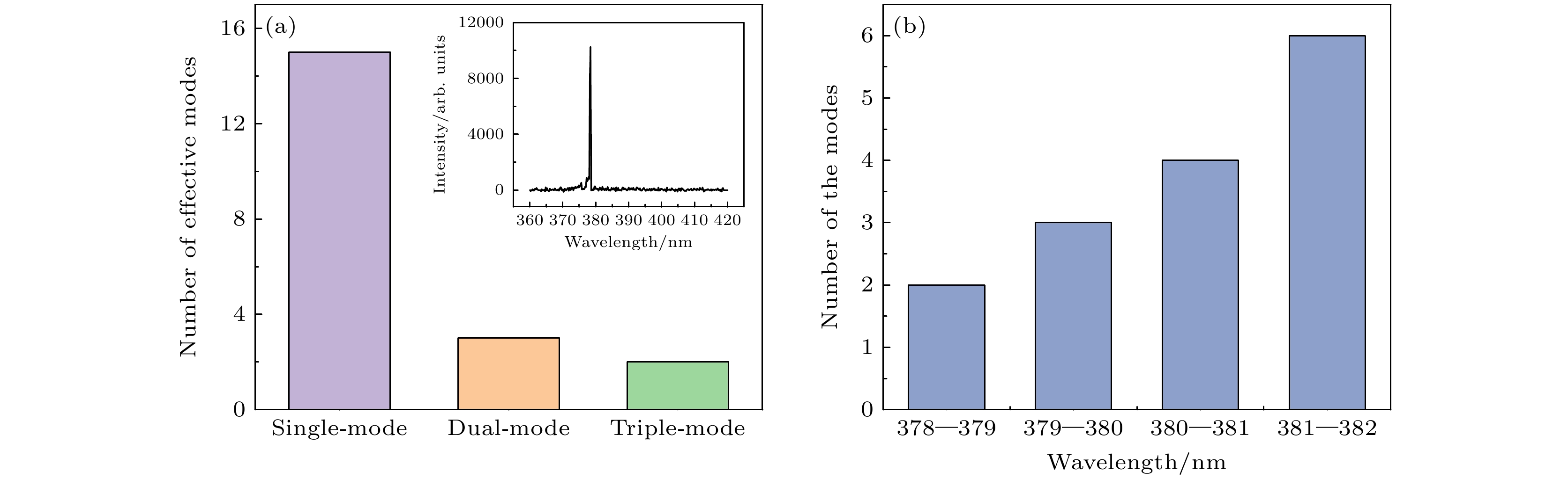
图 5 对于LED-2.5在注入电流为7 mA时采集的 20幅EL谱 (a) 出现单模、双模、三模激射的例数, 插图为出现单模激射的EL谱; (b) 单模激射的峰位分布情况
Fig. 5. For the 20 EL spectra of LED-2.5 acquired at the injection current of 7 mA: (a) Number of cases exhibiting single-mode, dual-mode or triple-mode lasing, the inset shows the EL spectrum of single-mode random lasing; (b) distribution of wavelengths for the single-mode lasing actions.
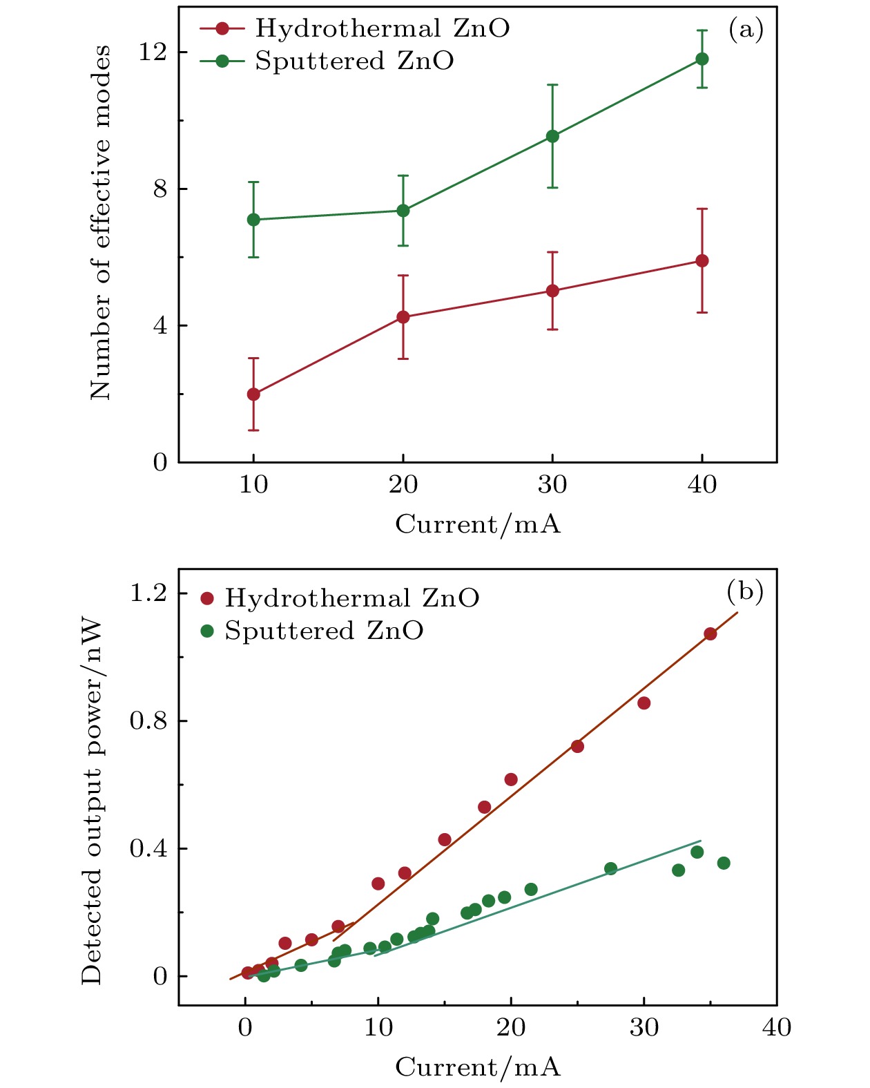
图 6 基于水热法和溅射法制备的ZnO薄膜的两种LED-2.5的电抽运随机激射 (a) 有效激射模式数随注入电流的变化情况; (b) 探测到的输出光功率随注入电流的变化关系曲线
Fig. 6. Electrically pumped random lasing actions from the two LED-2.5 respectively based on the hydrothermal and sputtered ZnO film: (a) Number of effective lasing modes as a function of the injection current; (b) curves of the detected output optical power changing with the injection current.
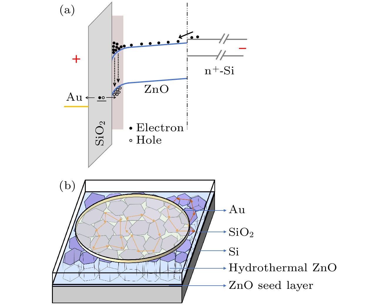
图 7 (a) 基于硅衬底上ZnO薄膜的MIS结构LED在足够高的正向偏压/注入电流下的能带结构示意图; (b) ZnO薄膜内光多重散射的示意图
Fig. 7. (a) Schematic diagram of the energy band structure for the MIS-structured LED using ZnO film on silicon substrate under sufficiently high forward bias/injection current; (b) schematic diagram of multiple light scattering within the ZnO film.
-
[1] Cao H, Zhao Y G, Ong H C, Ho S T, Dai J Y, Wu J Y, Chang R P H 1998 Appl. Phys. Lett. 73 3656
Google Scholar
[2] Yu S F, Leong E S P 2004 IEEE J. Quantum Electron. 40 1186
Google Scholar
[3] Cao H, Zhao Y G, Ong H C, Chang R P H 1999 Phys. Rev. B 59 15107
Google Scholar
[4] Thareja R K, Mitra A 2000 Appl. Phys. B: Lasers Opt. 71 181
Google Scholar
[5] Lau S P, Yang H Y, Yu S F, Li H D, Tanemura M, Okita T, Hatano H, Hng H H 2005 Appl. Phys. Lett. 87 013104
Google Scholar
[6] Ursaki V V, Burlacu A, Rusu E V, Postolake V, Tiginyanu I M 2009 J. Opt. A: Pure Appl. Opt. 11 075001
Google Scholar
[7] Yu S F, Yuen C, Lau S P, Park W I, Yi G C 2004 Appl. Phys. Lett. 84 3241
Google Scholar
[8] Ma X Y, Chen P L, Li D S, Zhang Y Y, Yang D R 2007 Appl. Phys. Lett. 91 251109
Google Scholar
[9] Chu S, Olmedo M, Yang Z, Kong J Y, Liu J L 2008 Appl. Phys. Lett. 93 181106
Google Scholar
[10] Long H, Fang G J, Huang H H, Mo X M, Xia W, Dong B Z, Meng X Q, Zhao X Z 2009 Appl. Phys. Lett. 95 013509
Google Scholar
[11] Zhu H, Shan C X, Zhang J Y, Zhang Z Z, Li B H, Zhao D X, Yao B, Shen D Z, Fan X W, Tang Z K, Hou X H, Choy K L 2010 Adv. Mater. 22 1877
Google Scholar
[12] Chen P L, Ma X Y, Li D S, Zhang Y Y, Yang D R 2009 Opt. Express 17 4712
Google Scholar
[13] Wang C X, Jiang H T, Li Y P, Ma X Y, Yang D R 2013 J. Appl. Phys. 114 133105
Google Scholar
[14] Wang C X, Zhu C, Lü C Y, Li D S, Ma X Y, Yang D R 2015 Appl. Surf. Sci. 332 620
Google Scholar
[15] Jiang S M, Xia C T, Ji R, Pang H W, Li D S, Yang D R, Ma X Y 2024 Acs Appl. Mater. Interfaces 16 3719
Google Scholar
[16] Ma X Y, Pan J W, Chen P L, Li D S, Zhang H, Yang Y, Yang D R 2009 Opt. Express 17 14426
Google Scholar
[17] Ryglowski L, Cyprych K, Mysliwiec J 2022 Opt. Commun. 510 127939
Google Scholar
[18] Li Y P, Wang C X, Jin L, Ma X Y, Yang D R 2013 Appl. Phys. Lett. 102 161112
Google Scholar
[19] 徐韵, 李云鹏, 金璐, 马向阳, 杨德仁 2013 62 084207
Google Scholar
Xu Y, Li Y P, Jin L, Ma X Y, Yang D R 2013 Acta Phys. Sin. 62 084207
Google Scholar
[20] Jiang X Y, Soukoulis C M 2000 Phys. Rev. Lett. 85 70
Google Scholar
[21] Sebbah P, Vanneste C 2002 Phys. Rev. B 66 144202
Google Scholar
[22] 杜文博, 冷进勇, 朱家健, 周朴, 许晓军, 舒柏宏 2012 61 114203
Google Scholar
Du W B, Leng J Y, Zhu J J, Zhou P, Xu X J, Shu B H 2012 Acta Phys. Sin. 61 114203
Google Scholar
[23] Zhu G Y, Tian M F, Almokhtar M, Qin F F, Li B H, Zhou M Y, Gao F, Yang Y, Ji X, He S Q, Wang Y J 2022 Chin. Phys. Lett. 39 123401 (in Chinese)
Google Scholar
[24] Liu H, Li S J, You Y Q, Wang J W, Sun J, Zhang L, Xiong L L 2023 Optik 281 170853
Google Scholar
[25] Wang Y Y, Xu C X, Jiang M M, Li J T, Dai J, Lu J F, Li P L 2016 Nanoscale 8 16631
Google Scholar
[26] 魏伟华, 李木天, 刘墨南 2018 67 064203
Google Scholar
Wei W H, Li M T, Liu M N 2018 Acta Phys. Sin. 67 064203
Google Scholar
[27] 马光辉, 张家斌, 张贺, 金亮, 王灌鑫, 徐英添 2019 中国光学 12 649
Google Scholar
Ma G H, Zhang J B, Zhang H, Jin L, Wang G X, Xu Y T 2019 Chin. Opt. 12 649
Google Scholar


 下载:
下载:


计量
- 文章访问数: 2789
- PDF下载量: 79
- 被引次数: 0
