-
电子空穴在库仑相互作用下会发生从半金属态到激子基态的相变, 在费米面附近自发打开能隙, 该基态被称为激子绝缘体. 该物态在凝聚态物理领域吸引了广泛的关注, 相关的实验证据一直在寻找中. 近年来, 在浅反转InAs/GaSb量子阱中, 激子绝缘体的光学能谱和输运特征首先被观察到, 证实了激子绝缘体在二维体系中的存在. 令人意外的是, 在这一激子绝缘态中, 电学输运测量探测到了对磁场和温度不敏感的一维类螺旋拓扑边缘态. 这一观察到的激子基态很难用现有的单粒子理论进行解释, 被称为拓扑激子绝缘体. 本文系统回顾了在该量子阱中针对拓扑激子绝缘体的实验研究, 包括电学输运、太赫兹透射谱、电容测量等. 这些实验结果综合表征了拓扑激子绝缘体的体态与边缘态性质. 拓扑激子绝缘体作为一个由玻色子构成的基态, 在极限条件下有望相变为具有宏观相干性的玻色爱因斯坦凝聚态, 为研究低维电子相互作用提供新的平台.Under Coulomb interactions, electrons and holes have a phase transition from a semi-metal state into an excitonic ground state, with a gap spontaneously opening at the Fermi level. The excitonic ground state is called excitonic insulator. The excitonic insulator has attracted extensive attention in condensed matter physics, but the experimental evidence of such a quantum state is still under search. Until recent years, optical spectral and transport evidence of the excitonic insulator has first been observed in shallowly inverted InAs/GaSb quantum wells, which confirms the existence of the exciton insulator in a two-dimensional system. Surprisingly, one-dimensional helical-like topological edge states, which are not sensitive to temperature nor magnetic field, have been observed in the excitonic insulator state by transport measurements. This new quantum phase cannot be well explained by existing single-particle theories, which is called a topological excitonic insulator. In this paper, we systematically review the experimental studies on the topological excitonic insulator in the InAs quantum well and GaAs quantum well, including magneto transport, terahertz transmission, capacitance, and Coulomb drag measurements. These experimental results comprehensively characterize the bulk properties and edge properties of the topological excitonic insulator. Furthermore, as a ground state consisting of bosons, the topological excitonic insulator is expected to have a quantum phase transition into Bose-Einstein condensate with macroscopic coherence under extreme conditions, which provides a new platform for studying the quantum phenomena of Coulomb interactions in low dimensions.
-
Keywords:
- excitonic insulator /
- quantum well /
- edge states
[1] Frenkel J 1931 Phys. Rev. 37 17
 Google Scholar
[2] Wannier G H 1937 Phys. Rev. 52 191
 Google Scholar
[3] Mott N F 1961 Philos. Mag. 6 287
 Google Scholar
[4] Keldysh L, Kopaev Y V 1965 Sov. Phys. Solid State 6 2219
[5] Jerome D, Rice T, Kohn W 1967 Phys. Rev. 158 462
 Google Scholar
[6] Du L J, Li X, Lou W, Sullivan G, Chang K, Kono J, Du R R 2017 Nat. Commun. 8 1971
 Google Scholar
[7] Halperin B, Rice T 1968 Rev. Mod. Phys. 40 755
 Google Scholar
[8] Lozovik Y E, Yudson V 1975 JETP Lett. 22 274
[9] Littlewood P, Zhu X 1996 Phys. Scr. 1996 56
[10] Zhu X, Littlewood P, Hybertsen M S, Rice T 1995 Phys. Rev. Lett. 74 1633
 Google Scholar
[11] Naveh Y, Laikhtman B 1996 Phys. Rev. Lett. 77 900
 Google Scholar
[12] Kroemer H 2004 Physica E 20 196
 Google Scholar
[13] Sakaki H, Chang L, Ludeke R, Chang C A, Sai-Halasz G, Esaki L 1977 Appl. Phys. Lett. 31 211
 Google Scholar
[14] Datta S, Melloch M, Gunshor R 1985 Phys. Rev. B 32 2607
[15] Cooper L, Patel N, Drouot V, Linfield E, Ritchie D, Pepper M 1998 Phys. Rev. B 57 11915
 Google Scholar
[16] Naveh Y, Laikhtman B 1995 Appl. Phys. Lett. 66 1980
 Google Scholar
[17] Liu C X, Hughes T L, Qi X L, Wang K, Zhang S C 2008 Phys. Rev. Lett. 100 236601
 Google Scholar
[18] Suzuki K, Harada Y, Onomitsu K, Muraki K 2013 Phys. Rev. B 87 235311
 Google Scholar
[19] Mueller S, Pal A N, Karalic M, Tschirky T, Charpentier C, Wegscheider W, Ensslin K, Ihn T 2015 Phys. Rev. B 92 081303
 Google Scholar
[20] Couedo F, Irie H, Suzuki K, Onomitsu K, Muraki K 2016 Phys. Rev. B 94 035301
 Google Scholar
[21] Irie H, Akiho T, Couedo F, Suzuki K, Onomitsu K, Muraki K 2020 Phys. Rev. Mater. 4 104201
[22] Knez I, Du R R, Sullivan G 2010 Phys. Rev. B 81 201301
 Google Scholar
[23] Knez I, Du R R, Sullivan G 2011 Phys. Rev. Lett. 107 136603
 Google Scholar
[24] Du L J, Li T X, Lou W K, Wu X J, Liu X X, Han Z D, Zhang C, Sullivan G, Ikhlassi A, Chang K, Du R R 2017 Phys. Rev. Lett. 119 056803
 Google Scholar
[25] Buttiker M 1986 Phys. Rev. Lett. 57 1761
 Google Scholar
[26] Buttiker M 1988 Phys. Rev. B 38 9375
 Google Scholar
[27] Pikulin D, Hyart T 2014 Phys. Rev. Lett. 112 176403
 Google Scholar
[28] Seradjeh B, Moore J, Franz M 2009 Phys. Rev. Lett. 103 066402
 Google Scholar
[29] Yang M J, Yang C H, Bennett B B, Shanabrook B V 1997 Phys. Rev. Lett. 78 4613
 Google Scholar
[30] Kono J, Mccombe B, Cheng J P, Lo I, Mitchel W, Stutz C 1997 Phys. Rev. B 55 1617
[31] Wang X, Belyanin A, Crooker S, Mittleman D, Kono J 2010 Nat. Phys. 6 126
[32] Zhang Q, Lou M, Li X, Reno J L, Pan W, Watson J D, Manfra M J, Kono J 2016 Nat. Phys. 12 1005
 Google Scholar
[33] Castella H, Wilkins J W 1998 Phys. Rev. B 58 16186
 Google Scholar
[34] Zhang Q, Wang Y R, Gao W L, Long Z Q, Watson J D, Manfra M J, Belyanin A, Kono J 2016 Phys. Rev. Lett. 117 207402
 Google Scholar
[35] Fenton E 1968 Phys. Rev. 170 816
 Google Scholar
[36] Kuramoto Y, Horie C 1978 Solid State Commun. 25 713
 Google Scholar
[37] Du L J, Knez I, Sullivan G, Du R R 2015 Phys. Rev. Lett. 114 096802
 Google Scholar
[38] Bernevig B A, Hughes T L, Zhang S C 2006 Science 314 1757
 Google Scholar
[39] Skolasinski R, Pikulin D I, Alicea J, Wimmer M 2018 Phys. Rev. B 98 201404
 Google Scholar
[40] Paul T, Becerra V F, Hyart T 2022 Phys. Rev. B 106 235420
 Google Scholar
[41] Xue F, Macdonald A H 2018 Phys. Rev. Lett. 120 186802
 Google Scholar
[42] Lopes N, Continentino M A, Barci D G 2022 Phys. Rev. B 105 165125
 Google Scholar
[43] Zeng Y, Xue F, Macdonald A H 2022 Phys. Rev. B 105 125102
 Google Scholar
[44] Blason A, Fabrizio M 2020 Phys. Rev. B 102 035146
 Google Scholar
[45] Saberi-Pouya S, Conti S, Perali A, Croxall A F, Hamilton A R, Peeters F M, Neilson D 2020 Phys. Rev. B 101 140501
 Google Scholar
[46] Varsano D, Palummo M, Molinari E, Rontani M 2020 Nat. Nanotechnol. 15 367
 Google Scholar
[47] Konig M, Wiedmann S, Brune C, Roth A, Buhmann H, Molenkamp L W, Qi X L, Zhang S C 2007 Science 318 766
 Google Scholar
[48] Chou Y Z, Nandkishore R M, Radzihovsky L 2018 Phys. Rev. B 98 054205
 Google Scholar
[49] Zhang S B, Zhang Y Y, Shen S Q 2014 Phys. Rev. B 90 115305
 Google Scholar
[50] Li C A, Zhang S B, Shen S Q 2018 Phys. Rev. B 97 045420
 Google Scholar
[51] Vayrynen J I, Goldstein M, Glazman L I 2013 Phys. Rev. Lett. 110 216402
 Google Scholar
[52] Ezawa Z F 2013 Quantum Hall Effects: Recent Theoretical and Experimental Developments (Vol. 3) (Singapore: World Scientific Publishing Company) pp370–388
[53] Klitzing K V, Dorda G, Pepper M 1980 Phys. Rev. Lett. 45 494
 Google Scholar
[54] Eisenstein J, Macdonald A 2004 Nature 432 691
 Google Scholar
[55] Du L J, Zheng J, Chou Y Z, Zhang J, Wu X, Sullivan G, Ikhlassi A, Du R R 2021 Nat. Electron. 4 573
 Google Scholar
[56] Narozhny B, Levchenko A 2016 Rev. Mod. Phys. 88 025003
 Google Scholar
[57] Nazarov Y V, Averin D 1998 Phys. Rev. Lett. 81 653
 Google Scholar
[58] Flensberg K 1998 Phys. Rev. Lett. 81 184
 Google Scholar
[59] Klesse R, Stern A 2000 Phys. Rev. B 62 16912
 Google Scholar
[60] Ponomarenko V, Averin D 2000 Phys. Rev. Lett. 85 4928
 Google Scholar
[61] Debray P, Zverev V, Raichev O, Klesse R, Vasilopoulos P, Newrock R 2001 J. Phys. Condens. Matter 13 3389
 Google Scholar
[62] Yamamoto M, Stopa M, Tokura Y, Hirayama Y, Tarucha S 2002 Physica E 12 726
 Google Scholar
[63] Yamamoto M, Stopa M, Tokura Y, Hirayama Y, Tarucha S 2006 Science 313 204
 Google Scholar
[64] Laroche D, Gervais G, Lilly M, Reno J 2011 Nat. Nanotechnol. 6 793
 Google Scholar
[65] Laroche D, Gervais G, Lilly M, Reno J 2014 Science 343 631
 Google Scholar
[66] Fiete G A, Le Hur K, Balents L 2006 Phys. Rev. B 73 165104
 Google Scholar
[67] Dmitriev A, Gornyi I, Polyakov D 2012 Phys. Rev. B 86 245402
 Google Scholar
[68] Chou Y Z, Levchenko A, Foster M S 2015 Phys. Rev. Lett. 115 186404
 Google Scholar
[69] Kainaris N, Gornyi I, Levchenko A, Polyakov D 2017 Phys. Rev. B, 95 045150
 Google Scholar
[70] Chou Y Z 2019 Phys. Rev. B 99 045125
 Google Scholar
[71] Syperek M, Stühler R, Consiglio A, Holewa P, Wyborski P, Dusanowski L, Reis F, Hofling S, Thomale R, Hanke W 2022 Nat. Commun. 13 6313
[72] Chen D, Lian Z, Huang X, Su Y, Rashetnia M, Ma L, Yan L, Blei M, Xiang L, Taniguchi T 2022 Nat. Phys. 18 1171
 Google Scholar
[73] Liu X, Li J, Watanabe K, Taniguchi T, Hone J, Halperin B I, Kim P, Dean C R 2022 Science 375 205
 Google Scholar
[74] Jia Y, Wang P, Chiu C L, et al. 2022 Nat. Phys. 18 87
 Google Scholar
[75] Ma L, Nguyen P X, Wang Z, et al. 2021 Nature 598 585
 Google Scholar
[76] Lee J, Kang C J, Eom M J, Kim J S, Min B I, Yeom H W 2019 Phys. Rev. B 99 075408
 Google Scholar
-
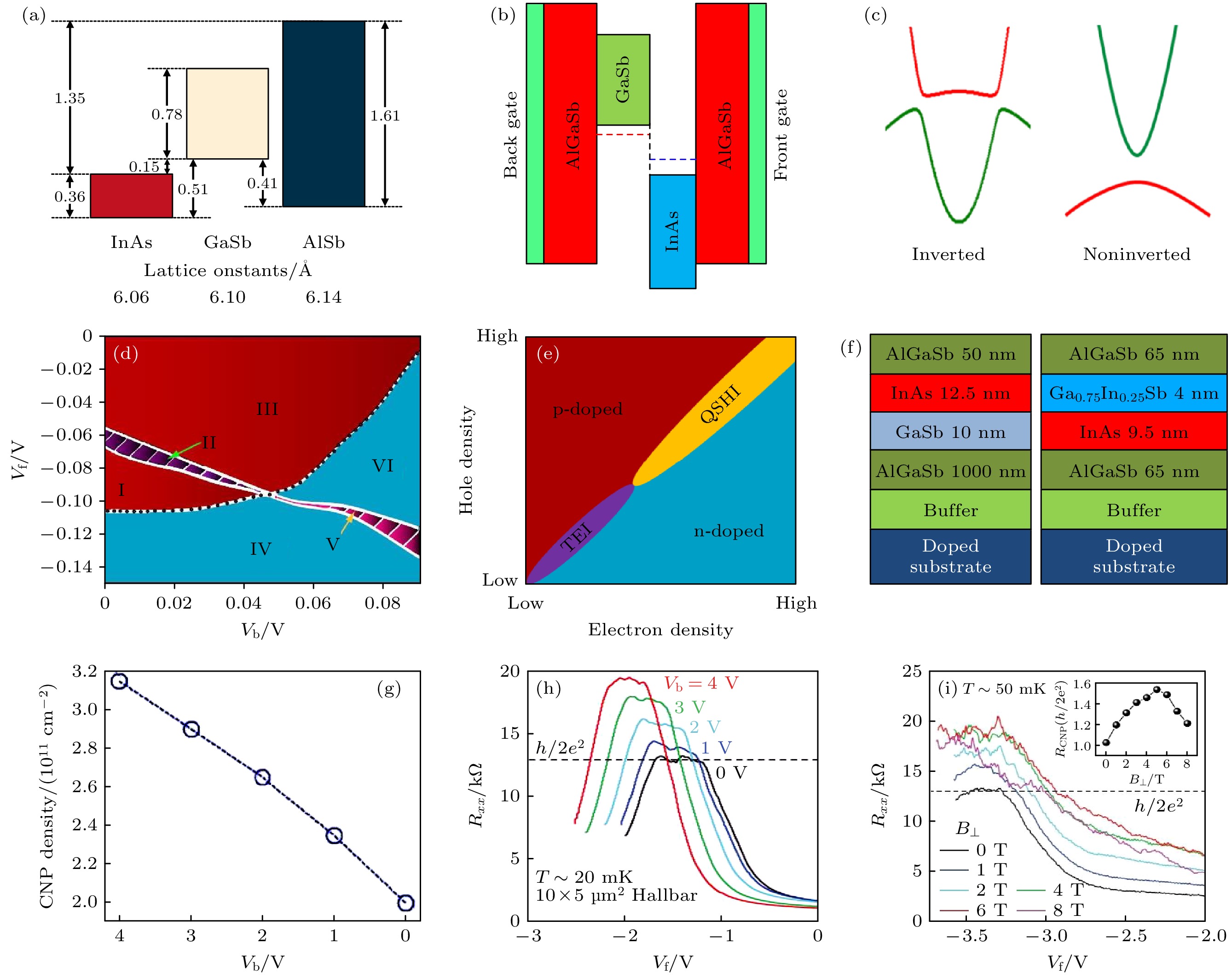
图 1 (a) 6.1 Å家族材料的能带排列和每种材料的晶格常数, 阴影部分表示能隙, 单位为eV [12]; (b) InAs/GaSb反转量子阱的能带示意图, 电子被限制在InAs层, 空穴被限制在GaSb层, 红色虚线表示空穴带顶, 蓝色虚线表示电子带底, 该图主要为体现材料间的能量关系, 未画出界面处的能带弯曲; (c) 反转能带和非反转能带结构示意图; (d) 系统物态关于前栅压和背栅压的相图, 区域I, II, III为反转区, 区域II为费米能在体态能隙中时的量子自旋霍尔相, 区域I, III分别为p, n型掺杂的反转体系, 区域IV, V, VI为非反转区, 区域V为费米能在体态能隙中时的普通绝缘体, 区域IV, VI分别为p, n型掺杂的普通半导体[17]; (e) 反转能带下不同电子空穴浓度时的相图, 远离电荷中性点(charge neutral point, CNP), 系统表现为p型掺杂(p-doped)或n型掺杂(n-doped), 电荷中性点附近, 高载流子浓度时系统为量子自旋霍尔绝缘体(quantum spin Hall insulator, QSHI), 低浓度时为拓扑激子绝缘体(topological exciton insulator, TEI); (f) 典型的InAs/GaSb和InAs/GaInSb量子阱结构; (g) InAs/GaInSb器件在不同背栅压下的电荷中性点载流子浓度; (h) InAs/GaInSb量子阱制备的10 μm×5 μm的霍尔型器件在不同背栅压下的Rxx-Vf曲线; (i) 背栅压为0 V时, InAs/GaInSb量子阱制备的3 μm×1.5 μm霍尔型器件在不同垂直磁场下的Rxx-Vf曲线, 插图为RCNP-B⊥曲线[24]
Fig. 1. (a) Band lineups in the 6.1 Å family material and the lattice constants of each material, the shaded parts show the energy gaps with all energies in eV[12]; (b) the band diagram of inverted InAs/GaSb quantum wells, the electrons are confined in InAs layer, and the holes are confined in GaSb layer, the red dashed line indicates the top of hole band, while the blue dashed line indicates the bottom of electron band, the figure mainly reflects the energy relationship between materials, and the energy bending at the interface is not showed; (c) schematic of inverted and non-inverted band structures; (d) the phase diagram for different front (Vf) and back (Vb) gate voltages. Regions I, II, III are in the inverted regime, in which the striped region II is the quantum spin Hall phase with the Fermi-level in the bulk gap, and I, III are the p-doped and n-doped inverted system. Regions IV, V, VI are in the normal regime, in which the striped region V is the insulating phase with the Fermi level in the bulk gap, and IV, VI are the p-doped and n-doped normal semiconductors[17]; (e) the phase diagram for electron and hole densities in the inverted band structure. Away from the charge neutral point, the system is p-doped or n-doped, near the charge neutral point, the system is a quantum spin Hall insulator at high charge densities and a topological exciton insulator at low charge densities; (f) typical InAs/GaSb and InAs/GaInSb wafer structures; (g) the charge neutral point density vs. back gate voltage traces in the InAs/GaInSb device; (h) Rxx vs. Vf traces measured from a 10 μm×5 μm Hall bar of InAs/GaInSb quantum wells under different back gate voltages; (i) Rxx vs. Vf traces measured from a 3 μm×1.5 μm Hall bar of InAs/GaInSb quantum wells under different perpendicular magnetic fields at Vb = 0 V. Inset: RCNP vs. B⊥ trace[24].
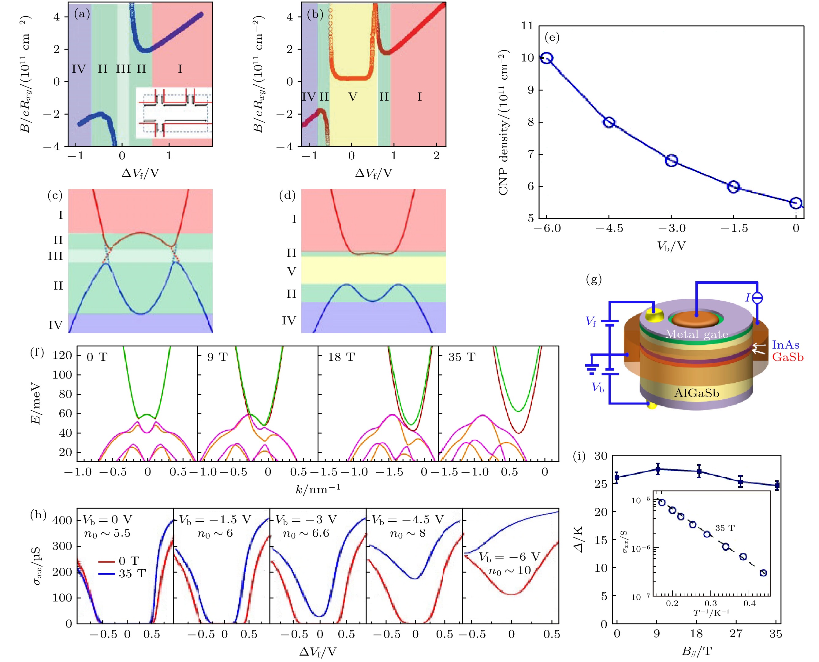
图 2 (a)—(d) 50 μm×50 μm非对称霍尔型器件的输运测量; (a), (b) Vb = 0 V和–6 V时B/(eRxy)随ΔVf的变化, 该数据在300 mK、外加1 T垂直磁场的条件下采集; (c), (d)分别为(a), (b)对应的能带, 红色区域I为电子主导区, 蓝色区域IV为空穴主导区, 绿色区域II为电子空穴共存区, 浅绿色区域III为杂化能隙, 虚线表示杂化能隙中剩余的电子和空穴, 金色区域V为激子绝缘体能隙, 插图为非对称霍尔型器件示意图, 虚线框内为前栅区域; (e) 电荷中性点处的载流子浓度随背栅压的变化; (f) 在B∥为0/9/18/35 T时, 经典反转能带中隧穿电子和空穴的色散关系, 计算采用8能带自洽模型; (g) Corbino测量装置示意图; (h) 在温度为30 mK, 平行磁场分别为0 T和35 T时, 不同载流子浓度的电导σxx-ΔVf曲线, 载流子浓度n0的单位为1010 cm–2; (i) Vb = 0 V时, 不同平行磁场下的能隙Δ, 误差提取自Arrhenius图中能隙的不确定度, 插图35 T时σxx极小值的Arrhenius图, 虚线为辅助线[6]
Fig. 2. (a)–(d) Magneto-transport in an asymmetric 50 μm × 50 μm Hall bar device; (a), (b), B/(eRxy) versus ΔVf for Vb = 0 and –6 V, respectively, the data were taken at 300 mK with a 1 T perpendicular magnetic field; (c), (d) show band alignments corresponding to (a), (b), respectively, the red regime I is the electron dominating regime, the blue regime IV is the hole dominating regime, the green regime II is the electron-hole coexisting regime, the light green regime III is the soft gap, the dotted line means residual electron and hole filling in hybridization gap, the gold regime V is the hard gap (excitonic insulator gap), inset is the schematic of the asymmetric Hallbar, and the region in the dashed box is covered by the front gate; (e) charge neutral point density as a function of back gate bias; (f) energy dispersions calculated with an 8-band self-consistent model for tunneling electrons and holes with a typical inverted band at B∥ = 0, 9, 18, 35 T; (g) schematic of the Corbino measurement; (h) density- dependent σxx-ΔVf traces under 0 T and 35 T in-plane magnetic fields at 30 mK, the value of n0 is noted in units of 1010 cm–2; (i) gap energy Δ vs. B∥ trace at zero back-gate bias, the error bars come from the uncertainty in extraction of gap energy from Arrhenius plot. Inset is Arrhenius plot of the conductance minimum σxx at 35 T. Dashed line is a guide to the eye[6].
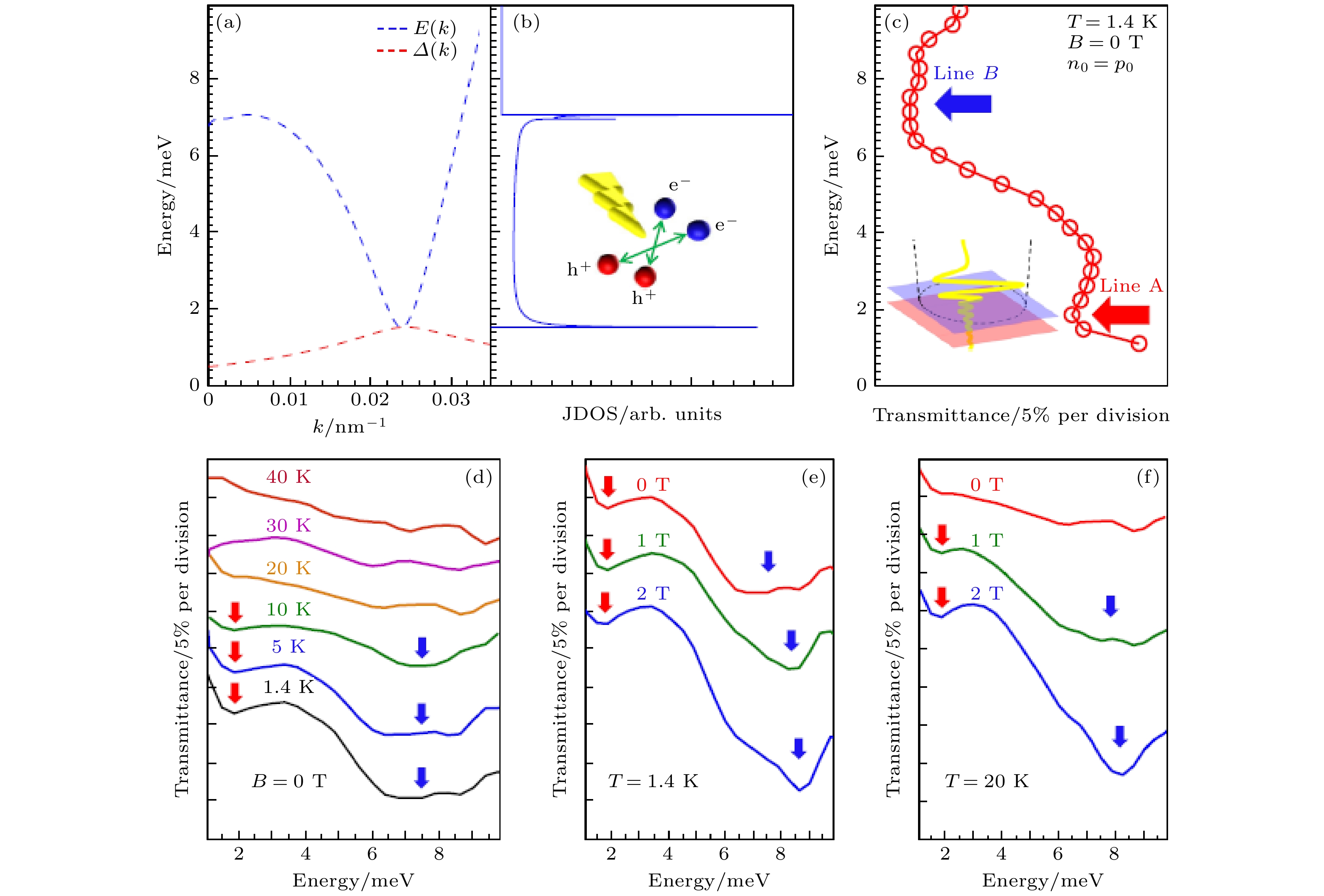
图 3 激子绝缘体的激子对破缺能谱和太赫兹透射实验 (a) Vb = 0 V时, 激子关于波矢k的能隙函数Δ(k)(红色虚线)和对破缺能量E(k)(蓝色虚线); (b) 联合态密度(JDOS)关于能量E的函数, 插图为太赫兹激光诱发的激子对破缺(蓝点表示电子, 红点表示空穴, 黄色箭头表示太赫兹入射光); (c) Vb = 0 V时, 在1.4 K, 0 T的电荷中性点处的太赫兹透射谱, 插图为紫色层为InAs量子阱, 红色层为GaSb量子阱, 黄色波浪线为太赫兹激光, 黑色虚线表示太赫兹入射光在样品上聚焦时的横向范围; (d) 0 T时, 不同温度下的透射谱; (e), (f) 1.4 K和20 K时, 不同磁场下的透射谱, 光谱在垂直方向上平移, 太赫兹能谱的测量误差为±0.2 meV[6]
Fig. 3. Pair-breaking excitation spectra and Terahertz transmission spectrum of excitonic insulator: (a) Gap function Δ(k) (red dashed line) and the pair-breaking energy E(k) (blue dashed line) of the exciton as a function of k for Vb = 0 V; (b) joint density of states (JDOS) as a function of energy. Inset: Pair-breaking induced by THz light (Blue dots are electrons, red dots are holes, yellow arrow is THz light); (c) transmission spectrum at the CNP at 1.4 K and 0 T for Vb = 0 V (Inset: The purple layer represents the InAs quantum well, the red layer represents the GaSb quantum well, the yellow wave indicates the THz light, the dashed black circle marks the lateral extent of the focused THz beam at the sample position); (d) transmittance spectra at various temperatures at 0 T; (e), (f) transmittance spectra at different magnetic fields at 1.4 and 20 K, respectively, the spectra are vertically offset for clarity, the measurement uncertainty in THz energy is ±0.2 meV[6].
图 4 (a) 电容测量的装置结构示意图; (b) 电容测量电路图; (c) Vb = 0 V(红线)和–6 V(蓝线)时的C-ΔVf曲线; (d) Vb = 0 V时, 不同温度(0.3, 2, 4, 6, 10 K)下的C-ΔVf曲线; (e) Vb = 0 V时, 能隙Δ随温度的变化, 红色数据点是基于Cq测量值得到的能隙, 虚线为计算得到的能隙. 误差棒来源于Cq和温度的不确定性[6]
Fig. 4. (a) Schematic of the structure for capacitance measurement; (b) diagram for capacitance measurement circuit; (c) C vs. ΔVf traces for Vb = 0 V (red line) and –6 V (blue line); (d) C vs. ΔVf curves under different temperatures (0.3 K, 2 K, 4 K, 6 K and 10 K) for Vb = 0 V; (e) Gap energy Δ vs. T trace for Vb = 0 V, at the charge-neutral point, the gap energies are extracted from Cq, the dotted dashed line is from the calculation, the error bars come from the uncertainties in Cq and the temperature[6].
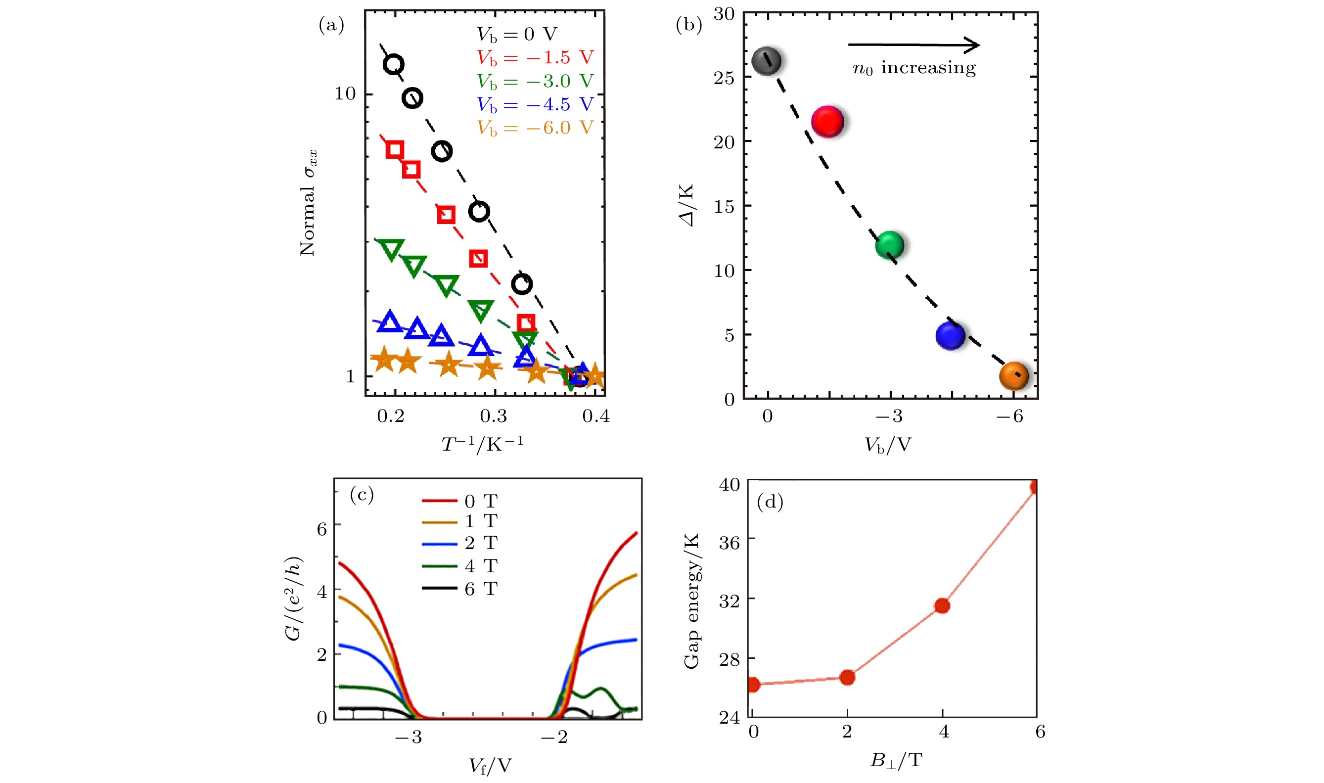
图 5 体态电导对背栅压和垂直磁场的依赖性 (a) 不同背栅压时电导最小值的Arrhenius图, 根据σxx ∝ exp(–Δ/2kBT)拟合得到Δ; 图中σxx根据2.5 K处的值归一化, 虚线为辅助线; (b) 能隙Δ-Vb[6]; (c) 300 mK时, Corbino器件在垂直磁场下测量到的电导G-Vf曲线; (d) G-B⊥曲线[37]
Fig. 5. Dependence of bulk conductance on back gate bias and perpendicular magnetic fields: (a) Arrhenius plot of the conductance minimum for different back-gate bias voltages, the data can be fit by σxx ∝ exp(–Δ/2kBT) to obtain Δ, here the σxx is normalized by its value at 2.5 K, dashed lines are guides to the eye; (b) measured gap energy Δ vs. Vb trace[6]; (c) G vs. Vf traces measured in Corbino device at T = 300 mK under perpendicular magnetic fields; (d) G vs. B⊥ traces[37].
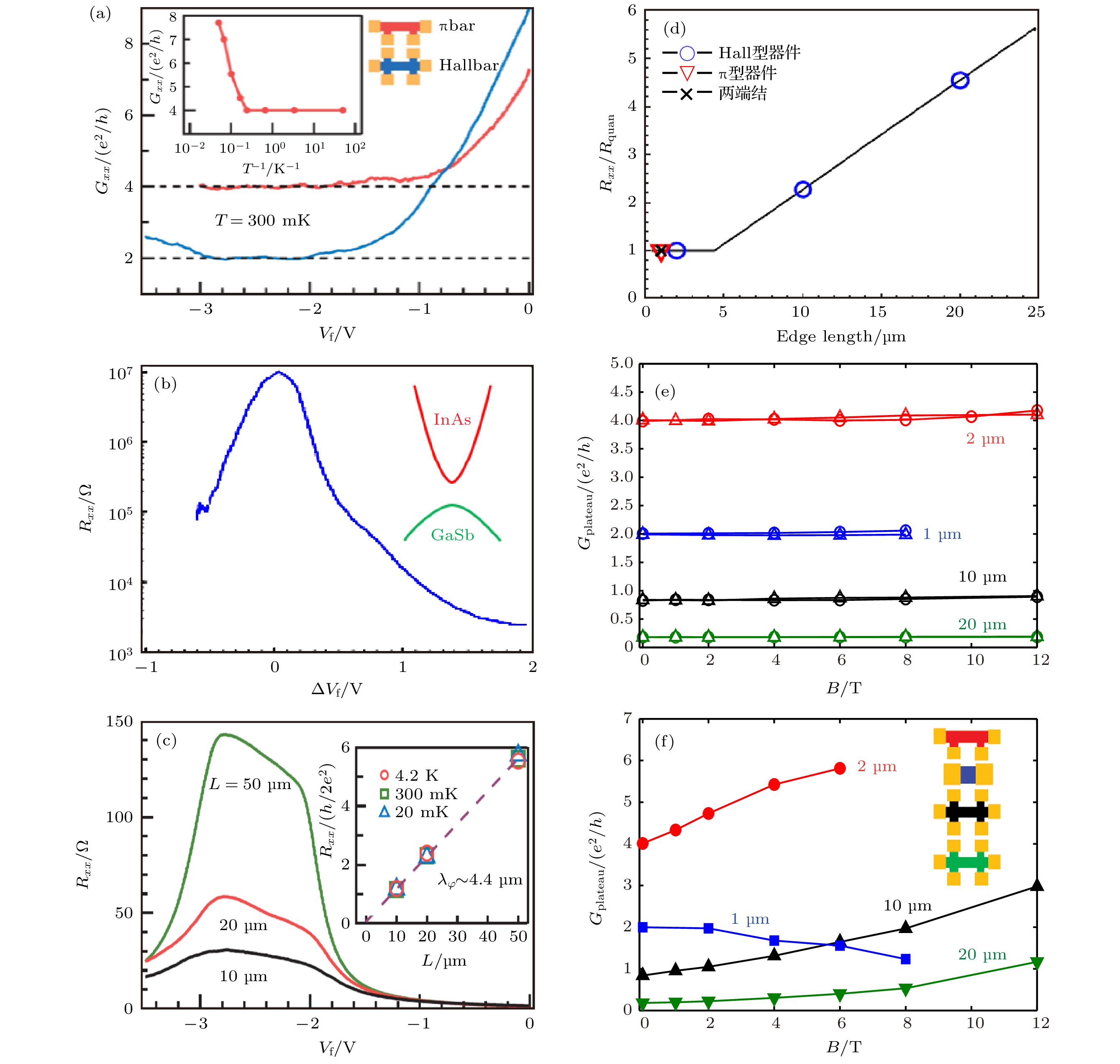
图 6 介观器件中的拓扑边缘态输运 (a) 在1 μm×2 μm的霍尔型器件和π型器件中, 分别测到量子化为2e2/h和4e2/h的宽电导平台, 插图为平台在温度低于4 K时保持稳定; (b) 在300 mK, 0 T时, 非反转量子阱的10 μm×20 μm霍尔器件中测得的Rxx-ΔVf曲线, 插图为非反转能带示意图; (c) 不同边缘长度的器件中的边缘电荷输运, 插图为不同温度下的Rxx-L曲线; (d) 在1 μm×1 μm两端结器件、1 μm×1 μm和1 μm×2 μm π型器件、1 μm×2 μm、5 μm×10 μm和10 μm×20 μm霍尔型器件中, Rxx-L曲线; (e), (f) 测量4种不同结构的器件的边缘态对磁场的依赖性, 对器件分别施加(e) 磁场方向平行(空心圆形)或垂直(空心三角形)于边缘轴向的平行面内磁场, (f) 垂直于量子阱平面的磁场[37]
Fig. 6. Topological edge transport in mesoscopic devices: (a) Wide conductance plateaus in 1 μm×2 μm Hallbar and π bar quantized to 2e2/h and 4e2/h, respectively (Inset: Plateau persists to 4 K); (b) measured Rxx vs. ΔVf trace in a 10 μm × 20 μm Hall bar from the noninverted quantum wells at 300 mK and 0 T (Inset: A sketch of noninverted band); (c) electrical charge transport in devices with different edge lengths (Inset: Rxx vs. device edge length L traces under different temperature); (d) Rxx vs. device edge length L traces in 1μm×1μm junction, 1 μm×1 μm and 1 μm×2 μm π bars, 1 μm×2 μm, 5 μm×10 μm and 10 μm×20 μm Hall bars; (e), (f) dependence of edge states under high magnetic fields in four different kinds of devices, an in-plane magnetic field (e) with a direction parallel (open circles) or perpendicular (open triangulars) to the edge axis and a perpendicular magnetic field (f) is applied to the device, respectively[37].
图 7 (a), (b) 正和负库仑拖曳, 红线和蓝线分别表示手性相反的边缘态; (c) 劈裂的H器件中, 有源驱动电路和拖曳电路的示意图, 驱动电路中, 电极3注入电流, 电极1接地. 拖曳电路中, 测量电极2与4间的电压. 绿框内为库仑拖曳的关键部分. 插图: H器件中间劈裂的空气间隙的扫描电子显微镜成像, 比例尺为100 nm; (d) 相邻两个边缘态的线性色散关系, 费米能在狄拉克点附近; (e), (f) 负和正库仑拖曳的净电流流向示意图, 虚线表示净电流方向, 驱动电路的设置与(c)一致[47]
Fig. 7. Positive (a) and negative (b) Coulomb drags, red and blue lines denote edge states with opposite chirality; (c) schematic of active drive circuit and drag circuit in a split H-bar, a current is injected into contact 3 with contact 1 grounded, and a voltage between contacts 2 and 4 is measured, the active part for Coulomb drag is highlighted by a green box (Inset: Scanning electron micrograph of the air gap in a split H-bar, scale bar is for 100 nm); (d) linearly dispersing energy band structures of two neighboring edges with the Fermi level around the Dirac point; (e), (f) current flow of the negative and positive drag, dashed lines show the current flow, the current is injected into the drive circuit in the same way as in (c)[47].
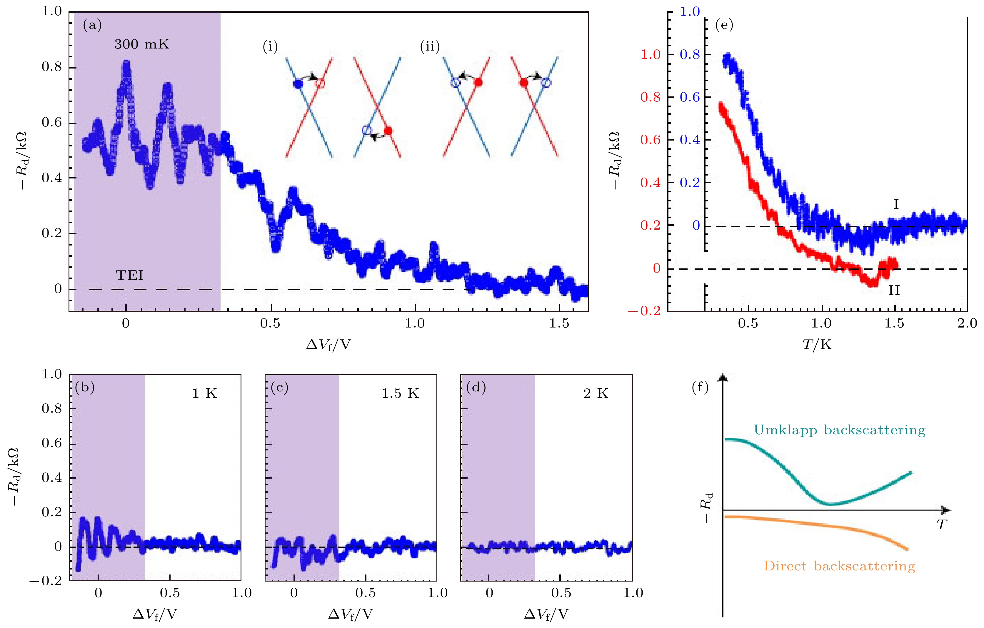
图 8 拓扑边缘态间的库仑拖曳信号对前栅压和温度的依赖性 在300 mK (a), 1 K (b), 1.5 K (c) 和2 K (d)下, 劈裂的H器件中边缘态的拖曳电阻随前栅压的变化, 将电阻信号最强处设为ΔVf = 0 V, 紫色阴影表示激子绝缘体区(插图(i)和(ii)分别描述了直接背散射和反转背散射机制), 蓝色和红色线对应具有线性色散关系的狄拉克能带, 实心/空心圆分别表示散射过程中的初始/最终状态; (e) 样品Ⅰ(蓝色)和样品Ⅱ(红色)在电荷中性点处拖曳电阻随温度的变化; (f)正负库仑拖曳电阻与温度的定性关系, 蓝绿色曲线表示反转背散射对负拖曳信号的贡献, 橙色曲线表示直接背散射对正拖曳信号的贡献[47]
Fig. 8. Front gate voltage and temperature dependence of Coulomb drag signals in topological edges: Drag resistance of edge states vs. front-gate voltage in the split H-bar device at 300 mK (a), 1 K (b), 1.5 K (c) and 2 K (d), the zero front-gate voltage is set at the value for which the resistance is the largest, purple-shaded areas indicate the topological exciton insulator regime (Insets: (i) and (ii) describe the direct and umklapp backscattering mechanisms, respectively), the blue and red lines correspond to linearly dispersing Dirac bands, filled/open circles represent initial/final states in scattering, respectively; (e) temperature dependence of the drag resistance at the CNP for sample Ⅰ (blue) and sample Ⅱ(red); (f) qualitatively sketched temperature dependence of positive and negative drag resistivity, the blue-green curve indicates the contribution of negative drag from umklapp backscattering and the orange curve represents the contribution of positive drag from direct backscattering[47].
-
[1] Frenkel J 1931 Phys. Rev. 37 17
 Google Scholar
[2] Wannier G H 1937 Phys. Rev. 52 191
 Google Scholar
[3] Mott N F 1961 Philos. Mag. 6 287
 Google Scholar
[4] Keldysh L, Kopaev Y V 1965 Sov. Phys. Solid State 6 2219
[5] Jerome D, Rice T, Kohn W 1967 Phys. Rev. 158 462
 Google Scholar
[6] Du L J, Li X, Lou W, Sullivan G, Chang K, Kono J, Du R R 2017 Nat. Commun. 8 1971
 Google Scholar
[7] Halperin B, Rice T 1968 Rev. Mod. Phys. 40 755
 Google Scholar
[8] Lozovik Y E, Yudson V 1975 JETP Lett. 22 274
[9] Littlewood P, Zhu X 1996 Phys. Scr. 1996 56
[10] Zhu X, Littlewood P, Hybertsen M S, Rice T 1995 Phys. Rev. Lett. 74 1633
 Google Scholar
[11] Naveh Y, Laikhtman B 1996 Phys. Rev. Lett. 77 900
 Google Scholar
[12] Kroemer H 2004 Physica E 20 196
 Google Scholar
[13] Sakaki H, Chang L, Ludeke R, Chang C A, Sai-Halasz G, Esaki L 1977 Appl. Phys. Lett. 31 211
 Google Scholar
[14] Datta S, Melloch M, Gunshor R 1985 Phys. Rev. B 32 2607
[15] Cooper L, Patel N, Drouot V, Linfield E, Ritchie D, Pepper M 1998 Phys. Rev. B 57 11915
 Google Scholar
[16] Naveh Y, Laikhtman B 1995 Appl. Phys. Lett. 66 1980
 Google Scholar
[17] Liu C X, Hughes T L, Qi X L, Wang K, Zhang S C 2008 Phys. Rev. Lett. 100 236601
 Google Scholar
[18] Suzuki K, Harada Y, Onomitsu K, Muraki K 2013 Phys. Rev. B 87 235311
 Google Scholar
[19] Mueller S, Pal A N, Karalic M, Tschirky T, Charpentier C, Wegscheider W, Ensslin K, Ihn T 2015 Phys. Rev. B 92 081303
 Google Scholar
[20] Couedo F, Irie H, Suzuki K, Onomitsu K, Muraki K 2016 Phys. Rev. B 94 035301
 Google Scholar
[21] Irie H, Akiho T, Couedo F, Suzuki K, Onomitsu K, Muraki K 2020 Phys. Rev. Mater. 4 104201
[22] Knez I, Du R R, Sullivan G 2010 Phys. Rev. B 81 201301
 Google Scholar
[23] Knez I, Du R R, Sullivan G 2011 Phys. Rev. Lett. 107 136603
 Google Scholar
[24] Du L J, Li T X, Lou W K, Wu X J, Liu X X, Han Z D, Zhang C, Sullivan G, Ikhlassi A, Chang K, Du R R 2017 Phys. Rev. Lett. 119 056803
 Google Scholar
[25] Buttiker M 1986 Phys. Rev. Lett. 57 1761
 Google Scholar
[26] Buttiker M 1988 Phys. Rev. B 38 9375
 Google Scholar
[27] Pikulin D, Hyart T 2014 Phys. Rev. Lett. 112 176403
 Google Scholar
[28] Seradjeh B, Moore J, Franz M 2009 Phys. Rev. Lett. 103 066402
 Google Scholar
[29] Yang M J, Yang C H, Bennett B B, Shanabrook B V 1997 Phys. Rev. Lett. 78 4613
 Google Scholar
[30] Kono J, Mccombe B, Cheng J P, Lo I, Mitchel W, Stutz C 1997 Phys. Rev. B 55 1617
[31] Wang X, Belyanin A, Crooker S, Mittleman D, Kono J 2010 Nat. Phys. 6 126
[32] Zhang Q, Lou M, Li X, Reno J L, Pan W, Watson J D, Manfra M J, Kono J 2016 Nat. Phys. 12 1005
 Google Scholar
[33] Castella H, Wilkins J W 1998 Phys. Rev. B 58 16186
 Google Scholar
[34] Zhang Q, Wang Y R, Gao W L, Long Z Q, Watson J D, Manfra M J, Belyanin A, Kono J 2016 Phys. Rev. Lett. 117 207402
 Google Scholar
[35] Fenton E 1968 Phys. Rev. 170 816
 Google Scholar
[36] Kuramoto Y, Horie C 1978 Solid State Commun. 25 713
 Google Scholar
[37] Du L J, Knez I, Sullivan G, Du R R 2015 Phys. Rev. Lett. 114 096802
 Google Scholar
[38] Bernevig B A, Hughes T L, Zhang S C 2006 Science 314 1757
 Google Scholar
[39] Skolasinski R, Pikulin D I, Alicea J, Wimmer M 2018 Phys. Rev. B 98 201404
 Google Scholar
[40] Paul T, Becerra V F, Hyart T 2022 Phys. Rev. B 106 235420
 Google Scholar
[41] Xue F, Macdonald A H 2018 Phys. Rev. Lett. 120 186802
 Google Scholar
[42] Lopes N, Continentino M A, Barci D G 2022 Phys. Rev. B 105 165125
 Google Scholar
[43] Zeng Y, Xue F, Macdonald A H 2022 Phys. Rev. B 105 125102
 Google Scholar
[44] Blason A, Fabrizio M 2020 Phys. Rev. B 102 035146
 Google Scholar
[45] Saberi-Pouya S, Conti S, Perali A, Croxall A F, Hamilton A R, Peeters F M, Neilson D 2020 Phys. Rev. B 101 140501
 Google Scholar
[46] Varsano D, Palummo M, Molinari E, Rontani M 2020 Nat. Nanotechnol. 15 367
 Google Scholar
[47] Konig M, Wiedmann S, Brune C, Roth A, Buhmann H, Molenkamp L W, Qi X L, Zhang S C 2007 Science 318 766
 Google Scholar
[48] Chou Y Z, Nandkishore R M, Radzihovsky L 2018 Phys. Rev. B 98 054205
 Google Scholar
[49] Zhang S B, Zhang Y Y, Shen S Q 2014 Phys. Rev. B 90 115305
 Google Scholar
[50] Li C A, Zhang S B, Shen S Q 2018 Phys. Rev. B 97 045420
 Google Scholar
[51] Vayrynen J I, Goldstein M, Glazman L I 2013 Phys. Rev. Lett. 110 216402
 Google Scholar
[52] Ezawa Z F 2013 Quantum Hall Effects: Recent Theoretical and Experimental Developments (Vol. 3) (Singapore: World Scientific Publishing Company) pp370–388
[53] Klitzing K V, Dorda G, Pepper M 1980 Phys. Rev. Lett. 45 494
 Google Scholar
[54] Eisenstein J, Macdonald A 2004 Nature 432 691
 Google Scholar
[55] Du L J, Zheng J, Chou Y Z, Zhang J, Wu X, Sullivan G, Ikhlassi A, Du R R 2021 Nat. Electron. 4 573
 Google Scholar
[56] Narozhny B, Levchenko A 2016 Rev. Mod. Phys. 88 025003
 Google Scholar
[57] Nazarov Y V, Averin D 1998 Phys. Rev. Lett. 81 653
 Google Scholar
[58] Flensberg K 1998 Phys. Rev. Lett. 81 184
 Google Scholar
[59] Klesse R, Stern A 2000 Phys. Rev. B 62 16912
 Google Scholar
[60] Ponomarenko V, Averin D 2000 Phys. Rev. Lett. 85 4928
 Google Scholar
[61] Debray P, Zverev V, Raichev O, Klesse R, Vasilopoulos P, Newrock R 2001 J. Phys. Condens. Matter 13 3389
 Google Scholar
[62] Yamamoto M, Stopa M, Tokura Y, Hirayama Y, Tarucha S 2002 Physica E 12 726
 Google Scholar
[63] Yamamoto M, Stopa M, Tokura Y, Hirayama Y, Tarucha S 2006 Science 313 204
 Google Scholar
[64] Laroche D, Gervais G, Lilly M, Reno J 2011 Nat. Nanotechnol. 6 793
 Google Scholar
[65] Laroche D, Gervais G, Lilly M, Reno J 2014 Science 343 631
 Google Scholar
[66] Fiete G A, Le Hur K, Balents L 2006 Phys. Rev. B 73 165104
 Google Scholar
[67] Dmitriev A, Gornyi I, Polyakov D 2012 Phys. Rev. B 86 245402
 Google Scholar
[68] Chou Y Z, Levchenko A, Foster M S 2015 Phys. Rev. Lett. 115 186404
 Google Scholar
[69] Kainaris N, Gornyi I, Levchenko A, Polyakov D 2017 Phys. Rev. B, 95 045150
 Google Scholar
[70] Chou Y Z 2019 Phys. Rev. B 99 045125
 Google Scholar
[71] Syperek M, Stühler R, Consiglio A, Holewa P, Wyborski P, Dusanowski L, Reis F, Hofling S, Thomale R, Hanke W 2022 Nat. Commun. 13 6313
[72] Chen D, Lian Z, Huang X, Su Y, Rashetnia M, Ma L, Yan L, Blei M, Xiang L, Taniguchi T 2022 Nat. Phys. 18 1171
 Google Scholar
[73] Liu X, Li J, Watanabe K, Taniguchi T, Hone J, Halperin B I, Kim P, Dean C R 2022 Science 375 205
 Google Scholar
[74] Jia Y, Wang P, Chiu C L, et al. 2022 Nat. Phys. 18 87
 Google Scholar
[75] Ma L, Nguyen P X, Wang Z, et al. 2021 Nature 598 585
 Google Scholar
[76] Lee J, Kang C J, Eom M J, Kim J S, Min B I, Yeom H W 2019 Phys. Rev. B 99 075408
 Google Scholar
计量
- 文章访问数: 8606
- PDF下载量: 454
- 被引次数: 0


 下载:
下载:
