


-
IV族元素锗材料由于具有电子和空穴迁移率高、禁带宽度小、与硅工艺相兼容等优势, 在低功耗高迁移率场效应晶体管领域具有广泛的应用潜力, 相应的Ge基金属-氧化物-半导体场效应晶体管(MOSFET)技术成为延续摩尔(more Moore)和超越摩尔(more than Moore)技术领域的前沿研究热点. 面向高迁移率的Ge基晶体管制备, 高质量栅极氧化物工艺是关键. 而高介电常数的Ge基栅极氧化物可以在提高栅控能力的同时, 有效降低器件栅极漏电, 提升器件的性能. 稀土系氧化物LaLuO3介电常数较高, 并且晶化温度高, 是制备Ge基MOSFET栅介质的优选方案. 本文通过磁控溅射技术制备Ge基氧化物LaLuO3介质, 并系统研究了退火工艺的气体种类、压强等氛围条件对Ge MOS栅电容特性的影响, 揭示了常压氧气氛围退火可以改善器件栅电容迟滞现象, 但存在栅界面层厚度增大的问题; 通过进一步发展基于高压低氧含量(0.1% O2)气体氛围退火技术, 在修复LaLuO3/Ge界面缺陷并减少氧空位产生的同时, 实现了极低的等效氧化层厚度(1.8 nm), 相应的LaLuO3/Ge MOS结构电容-电压曲线迟滞仅为 40 mV, 为Ge MOSFET提供了高性能LaLuO3/Ge栅极工艺方案.
-
关键词:
- Ge基金属-氧化物-半导体场效应晶体管 /
- 栅极结构工艺 /
- 稀土氧化物 /
- 高介电常数
Germanium material holds great potential applications in low-power, high-mobility field-effect transistors because of their advantages of high electron and hole mobility, narrow bandgap, and compatibility with silicon CMOS technologies. The development of high-quality gate oxide processes is crucial in fabricating high-mobility Ge-based transistors, especially those with high dielectric constant for superior gate control and preferable gate stability. Rare-earth oxides represented by LaLuO3 have high dielectric constants and high crystallization temperatures, making them potential candidates for Ge-based metal-oxide-semiconductor field-effect transistor (MOSFET) gate technology. In this work, a germanium (Ge)-based oxide dielectric LaLuO3 is fabricated utilizing a p-type Ge substrate with a (111) crystal orientation and a doping concentration of 1×1016 cm–3, and radio-frequency (RF) co-sputtering 2-inch 99.9% La2O3 and Lu2O3 targets. Systematical investigations are conducted to evaluate the effects of annealing process conditions on the characteristics of the LaLuO3/Ge MOS gate structure under three specifically designed annealing atmospheres, i.e. nitrogen, oxygen, and a nitrogen-oxygen mixed gas with an N2:O2 ratio of 0.999∶0.001. Meanwhile, the influence of annealing pressure is also explored. The results show that annealing in pure oxygen at atmospheric pressure can reduce the hysteresis of gate capacitance, but it can lead to the formation of interface layers. Correspondingly, annealing technique based on high-pressure and low-oxygen-content (0.1% O2) atmosphere is developed, which not only improves the LaLuO3/Ge interface quality and suppresses the oxygen vacancy generation, but also achieves an extremely low equivalent oxide thickness (EOT) of 1.8 nm and a hysteresis voltage of only 40 mV, resulting in an ideal LaLuO3/Ge MOS structure. This work thus provides a high-performance LaLuO3/Ge gate process solution for Ge MOSFETs.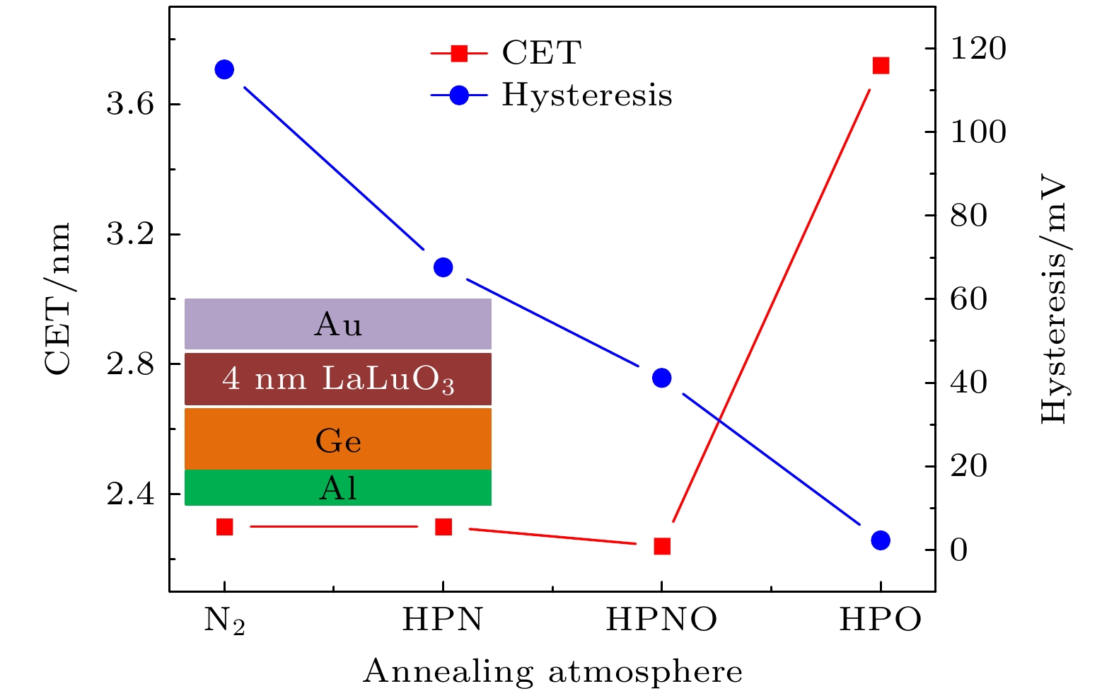
-
Keywords:
- Ge-based metal-oxide-semiconductor field-effect transistor /
- gate stack process /
- rare-earth oxide /
- high-k dielectric constant
[1] Del Alamo J A 2011 Nature 479 317
 Google Scholar
[2] 赵毅, 李骏康, 郑泽杰 2019 68 167301
Google Scholar
Zhao Y, Li J K, Zheng Z J 2019 Acta Phys. Sin. 68 167301
Google Scholar
[3] Wang S W, Guo H X, Ma T, Lei Z F, Ma W Y, Zhong X L, Zhang H, Lu X J, Li J F, Fang J L, Zeng T X 2024 Acta Phys. Sin. 73 238501 [王颂文, 郭红霞, 马腾, 雷志锋, 马武英, 钟向丽, 张鸿, 卢小杰, 李济芳, 方俊霖, 曾天祥 2024 73 238501]
Google Scholar
Wang S W, Guo H X, Ma T, Lei Z F, Ma W Y, Zhong X L, Zhang H, Lu X J, Li J F, Fang J L, Zeng T X 2024 Acta Phys. Sin. 73 238501
Google Scholar
[4] Shao Y J, Zhou J, Xu N, Chen J, Watanabe K, Taniguchi T, Shi Y, Li S L 2023 Chin. Phys. Lett. 40 068501
Google Scholar
[5] Yan N, Xiong Z R, Qin C B, Li X X 2024 Chin. Phys. Lett. 41 028101
Google Scholar
[6] 王琛, 温盼, 彭聪, 徐萌, 陈龙龙, 李喜峰, 张建华 2023 72 087302
Google Scholar
Wang C, Wen P, Peng C, Xu M, Chen L L, Li X F, Zhang J H 2023 Acta Phys. Sin. 72 087302
Google Scholar
[7] Wu H, Wu W, Si M, Peide D Y 2015 IEEE International Electron Devices Meeting (IEDM) Washington DC USA, December 7−9, 2015 p2.1.1
[8] Yu B, Chang L, Ahmed S, Wang H, Bell S, Yang C Y, Tabery C, Ho C, Xiang Q, King T J, Bokor J, Hu C, Lin M R, Kyser D 2002 IEEE International Electron Devices Meeting (IEDM) San Francisco, CA, USA, December 8−11, 2002 p10.2.1
[9] 曹磊, 刘红侠 2012 61 247303
Google Scholar
Cao L, Liu H 2012 Acta Phys. Sin. 61 247303
Google Scholar
[10] Kim J H, Kim S, Park B G 2019 IEEE Trans. Elec. Dev. 66 1656
Google Scholar
[11] 陈俊东, 韩伟华, 杨冲, 赵晓松, 郭仰岩, 张晓迪, 杨富华 2020 69 137701
Google Scholar
Chen J D, Han W H, Yang C, Zhao X S, Guo Y Y, Zhang X D, Yang F H 2020 Acta Phys. Sin. 69 137701
Google Scholar
[12] Liu C, Wang X Z, Shen C, Ma L P, Yang X Q, Kong Y, Ma W, Liang Y, Feng S, Wang X Y, Wei Y N, Zhu X, Li B, Li C Z, Dong S C, Zhang L N, Ren W C, Sun D M, Cheng H M 2024 Nature 632 782
Google Scholar
[13] Wei W J, Lü W F, Han Y, Zhang C Y, Chen D K 2023 Chin. Phys. B 32 097301
Google Scholar
[14] Takagi S, Zhang R, Suh J, Kim S H, Yokoyama M, Nishi K, Takenaka M 2015 Jpn. J. Appl. Phys. 54 06FA01
Google Scholar
[15] Kamata Y 2008 Mater. Today 11 30
Google Scholar
[16] Zhang R, Huang P C, Lin J C, Taoka N, Takenaka M, Takagi S 2013 IEEE Trans. Elec. Dev. 60 927
Google Scholar
[17] Nakaharai S, Tezuka T, Sugiyama N, Moriyama Y, Takagi S 2003 Appl. Phys. Lett. 83 3516
Google Scholar
[18] Chen C W, Tzeng J Y, Chung C T, Chien H P, Chien C H, Luo G L 2014 IEEE Trans. Elec. Dev. 61 2656
Google Scholar
[19] Zhang R, Tang X, Yu X, Li J, Zhao Y 2016 IEEE Elec. Dev. Lett. 37 831
Google Scholar
[20] Murad S A, Baine P T, McNeill D W, Mitchell S J N, Armstrong B M, Modreanu M, Hughes G, Chellappan R K 2012 Solid-state Electrons. 78 136
Google Scholar
[21] Lee C H, Nishimura T, Nagashio K, Kita K, Toriumi A 2011 IEEE Trans. Elec. Dev. 58 1295
Google Scholar
[22] Xie M, Nishimura T, Yajima T, Toriumi A 2020 J. Appl. Phys. 127 024101
Google Scholar
[23] Wang S K, Kita K, Nishimura T, Nagashio K, Toriumi A 2011 Jpn. J. Appl. Phys. 50 04DA01
Google Scholar
[24] Ogawa S, Suda T, Yamamoto T, Kutsuki K, Hideshima I, Hosoi T, Shimura T, Watanabe H 2011 Appl. Phys. Lett. 99 142101
Google Scholar
[25] Roeckerath M, Heeg T, Lopes J M J, Schubert J, Mantl S, Besmehn A, Myllymӓki P, Niinistö L 2008 Thin Solid Films 517 201
Google Scholar
[26] Goh K H, Haseeb A S M A, Wong Y H 2017 Mater. Sci. Semicon. Proc. 68 302
Google Scholar
[27] Gu J J, Liu Y Q, Xu M, Celler G K, Gordon R G, Ye P D 2010 Appl. Phys. Lett. 97 012106
Google Scholar
[28] Özben E D, Lopes J M J, Nichau A, Schnee M, Lenk S, Besmehn A, Bourdelle K K, Zhao Q T, Schubert J, Mantl S 2010 IEEE Elec. Dev. Lett. 32 15
Google Scholar
[29] Yu W J, Zhang B, Liu C, Xue Z Y, Chen M, Zhao Q T 2014 Chin. Phys. Lett. 31 016101
Google Scholar
[30] Xiong K, Robertson 2009 Microelectron. Eng. 86 1672
Google Scholar
[31] Radtke C, Krug C, Soares G V, Baumvol I J R, Lopes J M J, Durgun-Ozben E, Nichau A, Schubert J, Mantl S 2010 Electrochem. Solid-State Lett. 13 G37
Google Scholar
[32] Tabata T, Lee C H, Kita K, Toriumi A 2008 ECS Trans. 16 479
Google Scholar
[33] Lee C H, Tabata T, Nishimura T, Nagashio K, Toriumi A 2012 Appl. Phys. Lett. 5 114001
Google Scholar
-
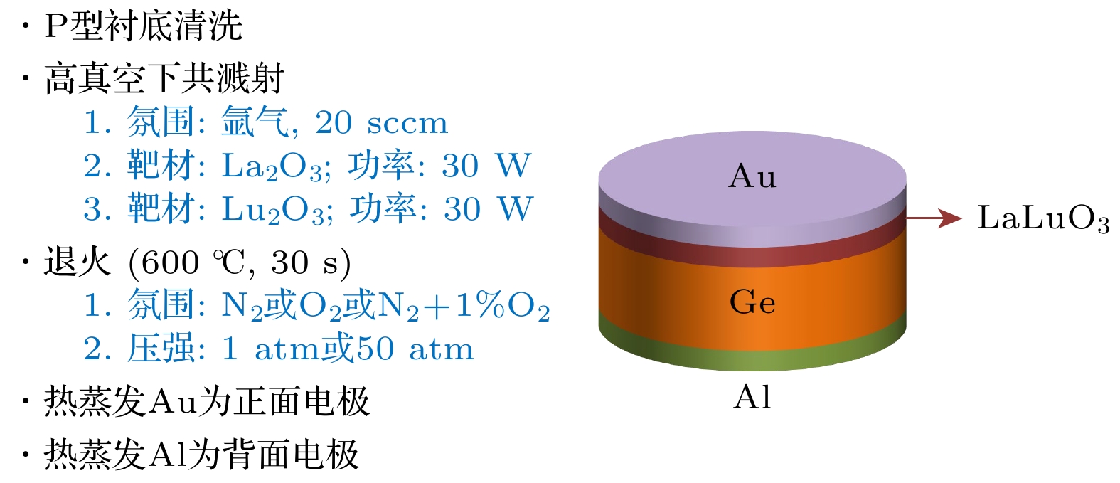
图 1 Au/LaLuO3/Ge/Al MOS电容制备工艺流程和器件结构示意图
Fig. 1. Fabrication process and device structure of Au/LaLuO3/Ge/Al MOS capacitor.
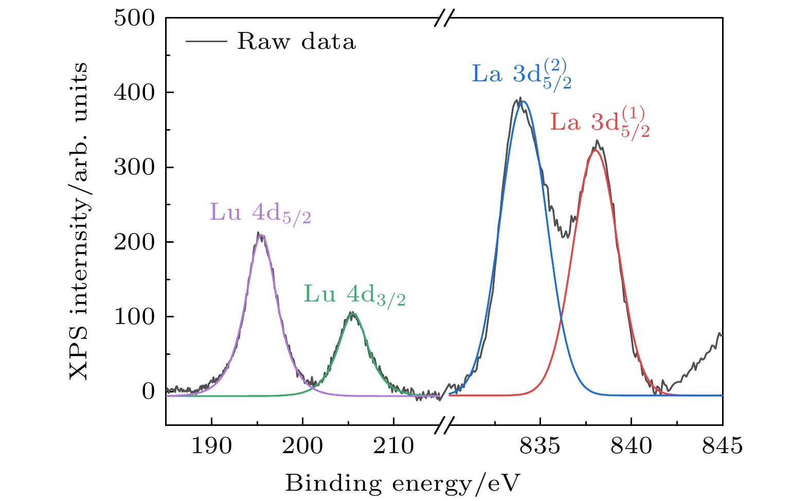
图 2 共溅射生成的30 nm LaLuO3薄膜的XPS测试数据与拟合峰
Fig. 2. XPS data and fitting peak curves for 30 nm LaLuO3 film by co-sputtering.
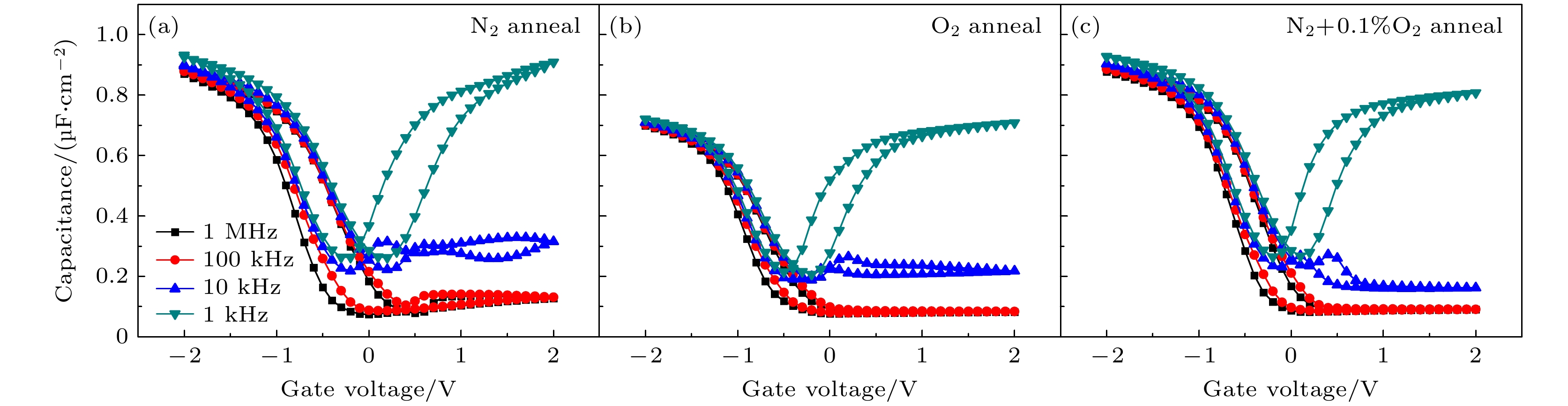
图 3 10 nm LaLuO3/Ge MOS 电容在不同环境下退火的电容-电压曲线(退火温度为600 ℃, 时间是30 s, 测试频率为 1 kHz—1 MHz) (a)氮气氛围; (b)氧气氛围; (c)低氧含量气体氛围
Fig. 3. The C -V curves of 10 nm LaLuO3/Ge MOS capacitors under different annealing atmosphere: (a) N2; (b) O2; (c) N2+0.1% O2. The annealing temperature is 600 ℃ and time is 30 s, with frequency changing from 1 kHz to 1 MHz.
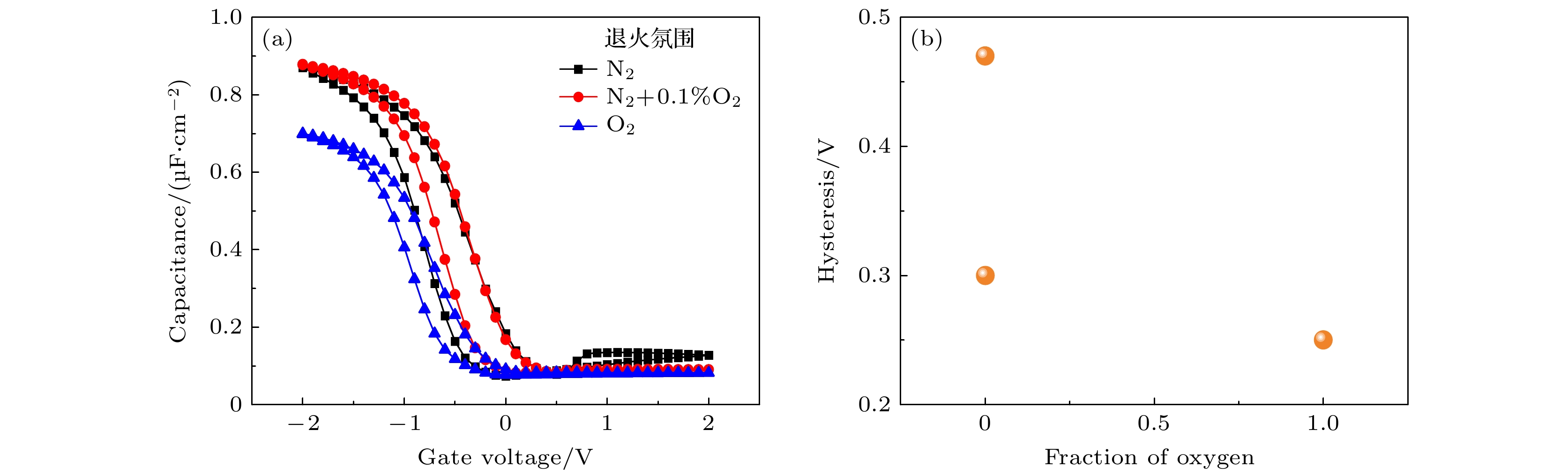
图 4 不同气体氛围下退火的LaLuO3/Ge MOS电容在1 MHz测试频率下的(a)电容-电压曲线和(b)迟滞电压
Fig. 4. The (a) C -V curves and (b) hysteresis values of LaLuO3/Ge MOS capacitors under different annealing atmospheres at frequency of 1 MHz
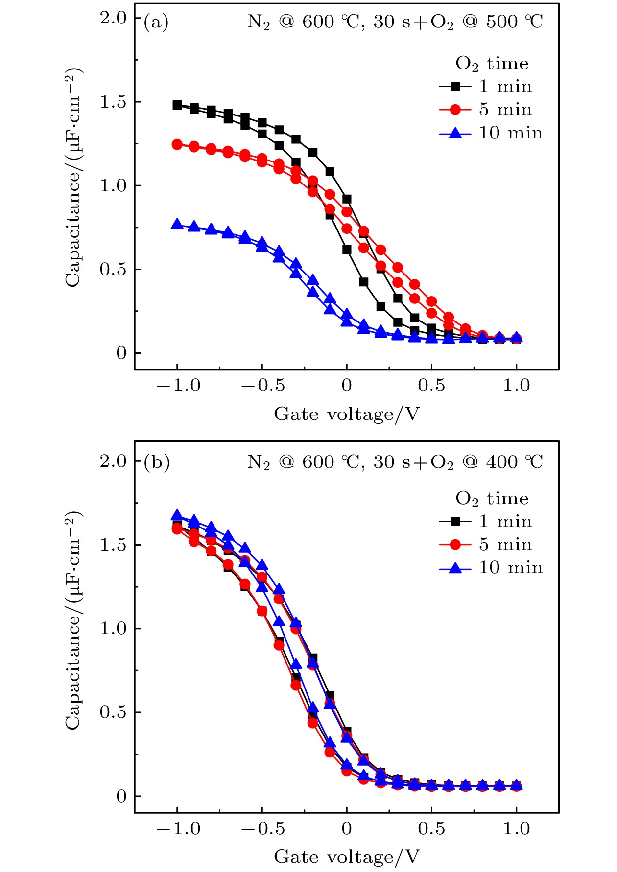
图 5 采用两步退火处理后的LaLuO3/Ge MOS电容的CV曲线, 第1步为600 ℃下氮气退火30 s , 第2步为氧气退火, 温度分别为(a) 500 ℃和(b) 400 ℃
Fig. 5. The C -V curves of LaLuO3/Ge MOS capacitors under two-stage annealing procedure, the first step is annealing in N2 ambient for 30 s at 600 ℃ and the second step is annealing in O2 ambient at (a) 500 ℃ and (b) 400 ℃.
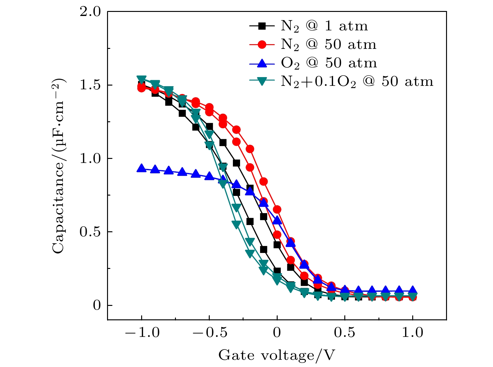
图 6 4 nm LaLuO3/Ge MOS 电容在不同环境下退火的电容-电压曲线, 测试频率为 1 MHz
Fig. 6. The C -V curves of 4 nm LaLuO3/Ge MOS capacitors under different annealing atmosphere at measuring frequency of 1 MHz.
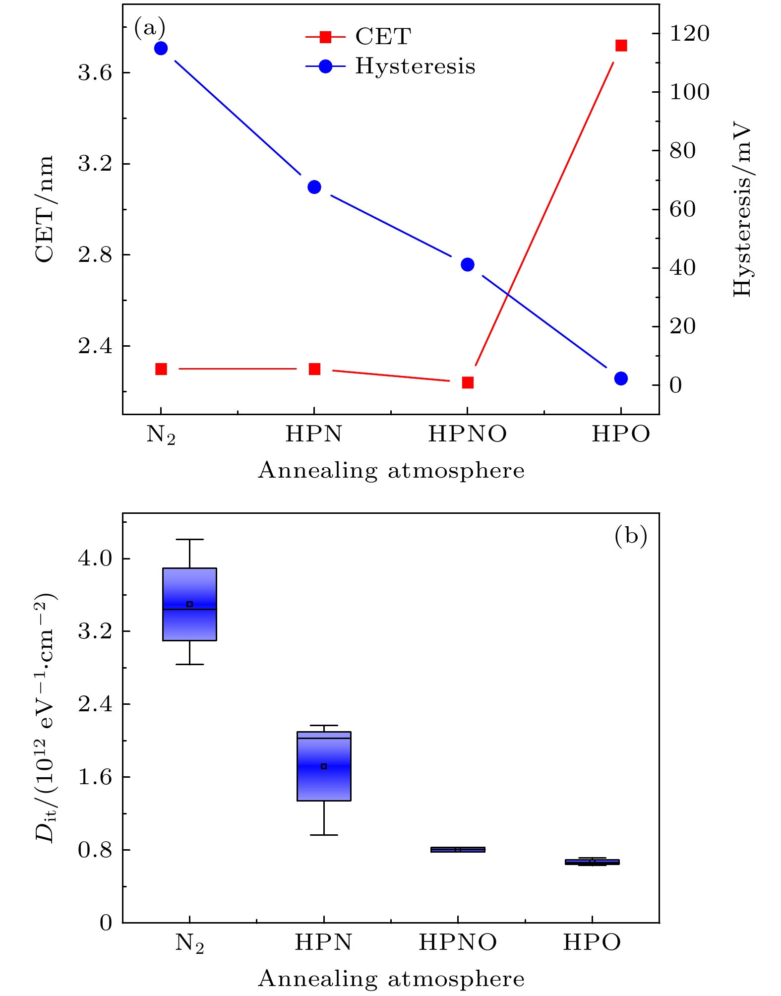
图 7 不同环境下退火的LaLuO3/Ge MOS 电容的(a) CET和迟滞, 以及(b)界面态密度Dit计算结果
Fig. 7. (a) CET and hysteresis and (b) Dit at Fermi level of LaLuO3/Ge MOS capacitors under different annealing atmosphere.
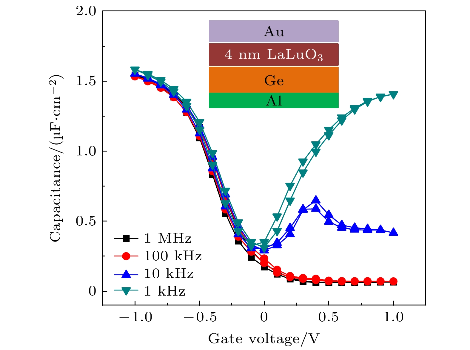
图 8 采用高压低氧含量(0.1%)气体退火后的4 nm LaLuO3/Ge MOS的电容-电压曲线
Fig. 8. The C -V characteristics of 4 nm LaLuO3/Ge MOS capacitors under high pressure N2+0.1%O2 mixture ambient.
-
[1] Del Alamo J A 2011 Nature 479 317
Google Scholar
[2] 赵毅, 李骏康, 郑泽杰 2019 68 167301
Google Scholar
Zhao Y, Li J K, Zheng Z J 2019 Acta Phys. Sin. 68 167301
Google Scholar
[3] Wang S W, Guo H X, Ma T, Lei Z F, Ma W Y, Zhong X L, Zhang H, Lu X J, Li J F, Fang J L, Zeng T X 2024 Acta Phys. Sin. 73 238501 [王颂文, 郭红霞, 马腾, 雷志锋, 马武英, 钟向丽, 张鸿, 卢小杰, 李济芳, 方俊霖, 曾天祥 2024 73 238501]
Google Scholar
Wang S W, Guo H X, Ma T, Lei Z F, Ma W Y, Zhong X L, Zhang H, Lu X J, Li J F, Fang J L, Zeng T X 2024 Acta Phys. Sin. 73 238501
Google Scholar
[4] Shao Y J, Zhou J, Xu N, Chen J, Watanabe K, Taniguchi T, Shi Y, Li S L 2023 Chin. Phys. Lett. 40 068501
Google Scholar
[5] Yan N, Xiong Z R, Qin C B, Li X X 2024 Chin. Phys. Lett. 41 028101
Google Scholar
[6] 王琛, 温盼, 彭聪, 徐萌, 陈龙龙, 李喜峰, 张建华 2023 72 087302
Google Scholar
Wang C, Wen P, Peng C, Xu M, Chen L L, Li X F, Zhang J H 2023 Acta Phys. Sin. 72 087302
Google Scholar
[7] Wu H, Wu W, Si M, Peide D Y 2015 IEEE International Electron Devices Meeting (IEDM) Washington DC USA, December 7−9, 2015 p2.1.1
[8] Yu B, Chang L, Ahmed S, Wang H, Bell S, Yang C Y, Tabery C, Ho C, Xiang Q, King T J, Bokor J, Hu C, Lin M R, Kyser D 2002 IEEE International Electron Devices Meeting (IEDM) San Francisco, CA, USA, December 8−11, 2002 p10.2.1
[9] 曹磊, 刘红侠 2012 61 247303
Google Scholar
Cao L, Liu H 2012 Acta Phys. Sin. 61 247303
Google Scholar
[10] Kim J H, Kim S, Park B G 2019 IEEE Trans. Elec. Dev. 66 1656
Google Scholar
[11] 陈俊东, 韩伟华, 杨冲, 赵晓松, 郭仰岩, 张晓迪, 杨富华 2020 69 137701
Google Scholar
Chen J D, Han W H, Yang C, Zhao X S, Guo Y Y, Zhang X D, Yang F H 2020 Acta Phys. Sin. 69 137701
Google Scholar
[12] Liu C, Wang X Z, Shen C, Ma L P, Yang X Q, Kong Y, Ma W, Liang Y, Feng S, Wang X Y, Wei Y N, Zhu X, Li B, Li C Z, Dong S C, Zhang L N, Ren W C, Sun D M, Cheng H M 2024 Nature 632 782
Google Scholar
[13] Wei W J, Lü W F, Han Y, Zhang C Y, Chen D K 2023 Chin. Phys. B 32 097301
Google Scholar
[14] Takagi S, Zhang R, Suh J, Kim S H, Yokoyama M, Nishi K, Takenaka M 2015 Jpn. J. Appl. Phys. 54 06FA01
Google Scholar
[15] Kamata Y 2008 Mater. Today 11 30
Google Scholar
[16] Zhang R, Huang P C, Lin J C, Taoka N, Takenaka M, Takagi S 2013 IEEE Trans. Elec. Dev. 60 927
Google Scholar
[17] Nakaharai S, Tezuka T, Sugiyama N, Moriyama Y, Takagi S 2003 Appl. Phys. Lett. 83 3516
Google Scholar
[18] Chen C W, Tzeng J Y, Chung C T, Chien H P, Chien C H, Luo G L 2014 IEEE Trans. Elec. Dev. 61 2656
Google Scholar
[19] Zhang R, Tang X, Yu X, Li J, Zhao Y 2016 IEEE Elec. Dev. Lett. 37 831
Google Scholar
[20] Murad S A, Baine P T, McNeill D W, Mitchell S J N, Armstrong B M, Modreanu M, Hughes G, Chellappan R K 2012 Solid-state Electrons. 78 136
Google Scholar
[21] Lee C H, Nishimura T, Nagashio K, Kita K, Toriumi A 2011 IEEE Trans. Elec. Dev. 58 1295
Google Scholar
[22] Xie M, Nishimura T, Yajima T, Toriumi A 2020 J. Appl. Phys. 127 024101
Google Scholar
[23] Wang S K, Kita K, Nishimura T, Nagashio K, Toriumi A 2011 Jpn. J. Appl. Phys. 50 04DA01
Google Scholar
[24] Ogawa S, Suda T, Yamamoto T, Kutsuki K, Hideshima I, Hosoi T, Shimura T, Watanabe H 2011 Appl. Phys. Lett. 99 142101
Google Scholar
[25] Roeckerath M, Heeg T, Lopes J M J, Schubert J, Mantl S, Besmehn A, Myllymӓki P, Niinistö L 2008 Thin Solid Films 517 201
Google Scholar
[26] Goh K H, Haseeb A S M A, Wong Y H 2017 Mater. Sci. Semicon. Proc. 68 302
Google Scholar
[27] Gu J J, Liu Y Q, Xu M, Celler G K, Gordon R G, Ye P D 2010 Appl. Phys. Lett. 97 012106
Google Scholar
[28] Özben E D, Lopes J M J, Nichau A, Schnee M, Lenk S, Besmehn A, Bourdelle K K, Zhao Q T, Schubert J, Mantl S 2010 IEEE Elec. Dev. Lett. 32 15
Google Scholar
[29] Yu W J, Zhang B, Liu C, Xue Z Y, Chen M, Zhao Q T 2014 Chin. Phys. Lett. 31 016101
Google Scholar
[30] Xiong K, Robertson 2009 Microelectron. Eng. 86 1672
Google Scholar
[31] Radtke C, Krug C, Soares G V, Baumvol I J R, Lopes J M J, Durgun-Ozben E, Nichau A, Schubert J, Mantl S 2010 Electrochem. Solid-State Lett. 13 G37
Google Scholar
[32] Tabata T, Lee C H, Kita K, Toriumi A 2008 ECS Trans. 16 479
Google Scholar
[33] Lee C H, Tabata T, Nishimura T, Nagashio K, Toriumi A 2012 Appl. Phys. Lett. 5 114001
Google Scholar


 下载:
下载:


计量
- 文章访问数: 2236
- PDF下载量: 49
- 被引次数: 0
