


-
在SrTiO3基氧化物异质结中, 由于Ti 3d轨道的影响, 界面处的二维电子气(2DEG)室温迁移率较低, 这限制了它们在半导体器件中的应用. 而SnO2的导带底由Sn的5s轨道组成, 因此, 基于SnO2的异质结界面具有形成室温下高迁移率2DEG的潜力. 本文采用第一性原理计算的方法, 对(001) HfO2/SnO2异质结构的界面电子结构进行了系统研究. 计算结果表明, 无缺陷的HfO2/SnO2异质结具有半导体的能带结构, 其界面附近不会形成2DEG. 当异质结界面附近的SnO2侧存在氧空位时, 体系出现跳跃导电, 但其界面附近仍不会出现2DEG. 当氧空位处于异质结的HfO2表面时, 氧空位的存在使表面产生缺陷态. 缺陷态的电子处于局域态, 并不参与导电, 但缺陷态与异质结构的导带底(由界面贡献) 发生交叠, 使异质结表面缺陷态中的电子转移至界面, 并在异质结界面附近形成2DEG. 此外, 对于HfO2层较薄的HfO2/SnO2异质结构, 比如HfO2层为7个单胞(约2.37 nm)厚时, HfO2表面吸附的H原子向异质结提供电子, 这些电子部分转移到界面附近的导带, 形成2DEG. 随着HfO2层厚度的增加, 表面电子转移到界面的概率逐渐下降, 使得界面处的电子浓度逐渐降低.In SrTiO3-based oxide heterostructures, the mobility of the two-dimensional electron gas (2DEG) at the interface is relatively low at room temperature due to the influence of Ti 3d orbitals, which limits their applications in semiconductor devices. In contrast, the conduction band bottom of SnO2 is composed of Sn 5s orbitals, and it has been demonstrated that bulk SnO2 exhibits high carrier mobility at room temperature. Therefore, SnO2-based heterostructure interfaces have the potential to form 2DEG with high mobility at room temperature. In this paper, we construct a heterostructure (HfO2)7/(SnO2)13 with $2 \times 1$ supercell in (001) plane and systematically investigate the electronic structure of the heterostructure by using first-principles calculations. The calculation results show that the defect-free (HfO2)7/(SnO2)13 heterostructure has a band structure similar to that of a semiconductor, and there is no 2DEG near the interface of the heterostructure. However, the conduction band bottom is mainly contributed by non-degenerate Sn 5s orbitals in this situation. In the in-plane $2 \times 1$ supercell of the (HfO2)7/(SnO2)13 heterostructure, each layer contains 8 oxygen atoms (the thickness of 1 unit cell is defined as a layer). When an oxygen atom in a layer on the SnO2 side near the interface of the heterostructure is removed, the presence of the oxygen vacancy leads to the formation of a defect band below the conduction band. This will lead to hopping conductivity in the heterostructure. However, 2DEG still does not appear near the heterostructure interface. When the oxygen vacancy is located in the surface layer of the HfO2 in the supercell structure, the presence of the oxygen vacancy leads to the formation of a defect state in the surface. The electrons in the defect state are localized and do not contribute to conductivity. However, the defect band overlaps with the conduction band at the interface, causing the electrons on the surface of HfO2 to tunnel towards the interface. In this scenario, the 2DEG emerges in the vicinity of the heterostructure interface. In addition, for HfO2/SnO2 heterostructures with thinner HfO2 layers, such as HfO2 layer with a thickness of 7 unit cells (about 2.37 nm), the H atoms adsorbed on the HfO2 surface provide electrons for the heterostructure. Some of these electrons transfer to the conduction band near the interface, leading to the formation of a 2DEG in that region. Meanwhile, the remaining electrons stay on the surface, forming a conductive layer with a thickness of approximately 2 unit cells. As the thickness of the HfO2 layer increases, the probability of electrons transferring from the surface to the interface gradually decreases, resulting in a gradual decrease in the electron density at the interface.
[1] Ohtomo A, Hwang H Y 2004 Nature 427 423
 Google Scholar
[2] Tampo H, Shibata H, Matsubara K, Yamada A, Fons P, Niki S, Yamagata M, Kanie H 2006 Appl. Phys. Lett. 89 132113
Google Scholar
[3] Hotta Y, Susaki T, Hwang H Y 2007 Phys. Rev. Lett. 99 236805
Google Scholar
[4] Chen Y Z, Bovet N, Trier F, Christensen D V, Qu F M, Andersen N H, Kasama T, Zhang W, Giraud R, Dufouleur J, Jespersen T S, Sun J R, Smith A, Nygård J, Lu L, Büchner B, Shen B G, Linderoth S, Pryds N 2013 Nat. Commun. 4 1371
Google Scholar
[5] Zou K, Ismail-Beigi S, Kisslinger K, Shen X, Su D, Walker F J, Ahn C H 2015 APL Mater. 3 036104
Google Scholar
[6] Zhang Y W, Neal A, Xia Z B, Joishi C, Johnson J M, Zheng Y H, Bajaj S, Brenner M, Dorsey D, Chabak K, Jessen G, Hwang J, Mou S, Heremans J P, Rajan S 2018 Appl. Phys. Lett. 112 173502
Google Scholar
[7] 颜送灵, 唐黎明, 赵宇清 2016 65 077301
Google Scholar
Yan S L, Tang L M, Zhao Y Q 2016 Acta Phys. Sin. 65 077301
Google Scholar
[8] Zhang H R, Yun Y, Zhang X J, Zhang H, Ma Y, Yan X, Wang F, Li G, Li R, Khan T, Chen Y S, Liu W, Hu F X, Liu B G, Shen B G, Han W, Sun J R 2018 Phys. Rev. Lett. 121 116803
Google Scholar
[9] Kozuka Y, Tsukazaki A, Maryenko D, Falson J, Akasaka S, Nakahara K, Nakamura S, Awaji S, Ueno K, Kawasaki M 2011 Phys. Rev. B 84 033304
Google Scholar
[10] Chen Z, Liu Y, Zhang H, Liu Z R, Tian H, Sun Y Q, Zhang M, Zhou Y, Sun J R, Xie Y W 2021 Science 372 721
Google Scholar
[11] 王继光, 李珑玲, 邱嘉图, 陈许敏, 曹东兴 2023 72 176801
Google Scholar
Wang J G, Li L L, Qiu G T, Chen X M, Cao D X 2023 Acta Phys. Sin. 72 176801
Google Scholar
[12] Thiel S, Hammerl G, Schmehl A, Schneider C W, Mannhart J 2006 Science 313 1942
Google Scholar
[13] Chen X H, Li Z Q, Hu Z X, Gao K H 2022 Phys. Rev. B 105 205437
Google Scholar
[14] Nakano M, Tsukazaki A, Ueno K, Gunji R Y, Ohtomo A, Fukumura T, Kawasaki M 2010 Appl. Phys. Lett. 96 052116
Google Scholar
[15] 张阳, 顾书林, 叶建东, 黄时敏, 顾然, 陈斌, 朱顺明, 郑有炓 2013 62 150202
Google Scholar
Zhang Y, Gu S L, Ye J D, Huang S M, Gu R, Chen B, Zhu S M, Zhen Y D 2013 Acta Phys. Sin. 62 150202
Google Scholar
[16] Himmetoglu B, Janotti A, Peelaers H, Alkauskas A, Van de Walle C G 2014 Phys. Rev. B 90 241204
Google Scholar
[17] Himmetoglu B, Janotti A 2016 J. Phys. Condens. Matter 28 065502
Google Scholar
[18] Lee J, Demkov A A 2008 Phys. Rev. B 78 193104
Google Scholar
[19] Chen X H, Li Z Q, Hou D Y, Hu Z X, Gao K H 2023 Phys. Rev. B 107 165411
Google Scholar
[20] Sanon G, Rup R, Mansingh A 1991 Phys. Rev. B 44 5672
Google Scholar
[21] Toyosaki H, Kawasaki M, Tokura Y 2008 Appl. Phys. Lett. 93 132109
Google Scholar
[22] Paudel T R, Tsymbal E Y 2017 Phys. Rev. B 96 245423
Google Scholar
[23] Nazir S, Cheng J L, Yang K S 2016 ACS Appl. Mater. Interfaces 8 390
Google Scholar
[24] Lee B H, Kang L, Nieh R, Qi W J, Lee J C 2000 Appl. Phys. Lett. 76 1926
Google Scholar
[25] Seo M, Kim S K, Han J H, Hwang C S 2010 Chem. Mater. 22 4419
Google Scholar
[26] Seo M, Kim S K, Min Y S, Hwang C S 2011 J. Mater. Chem. 21 18497
Google Scholar
[27] Blöchl P E 1994 Phys. Rev. B 50 17953
Google Scholar
[28] Kresse G, Hafner J 1993 Phys. Rev. B 47 558
Google Scholar
[29] Kresse G, Furthmüller J 1996 Phys. Rev. B 54 11169
Google Scholar
[30] Kresse G, Joubert D 1999 Phys. Rev. B 59 1758
Google Scholar
[31] Gilani R, Rehman S U, Butt F K, Haq B U, Aleem F 2018 Silicon 10 2317
Google Scholar
[32] Singh A K, Janotti A, Schefler M, Van de Walle C G 2008 Phys. Rev. Lett. 101 055502
Google Scholar
[33] Park J, Saidi W A, Chorpening B, Duan Y H 2021 J. Phys. Chem. C 125 22231
Google Scholar
[34] Marcillo F, Stashans A 2015 J. Theor. Comput. Chem. 13 1450069
Google Scholar
[35] Heyd J, Peralta J E, Scuseria G E, Martin R L 2005 J. Chem. Phys. 123 174101
Google Scholar
[36] Pavoni E, Mohebbi E, Stipa P, Mencarelli D, Pierantoni L 2022 Materials 15 4175
Google Scholar
[37] Akbar W, Elahi I, Nazir S 2020 J. Magn. Magn. Mater. 511 166948
Google Scholar
[38] Li J P, Meng S H, Yang C, Lu H T, Tohyama T 2018 Chin. Phys. B 27 027101
Google Scholar
[39] Krishnaswamy K, Himmetoglu B, Kang Y, Janotti A, Van de Walle C G 2017 Phys. Rev. B 95 205202
Google Scholar
[40] Herranz G, Basletić M, Bibes M, Carrétéro C, Tafra E, Jacquet E, Bouzehouane K, Deranlot C, HamzićA, Broto J M, Barthélémy A, Fert A 2007 Phys. Rev. Lett. 98 216803
Google Scholar
[41] Oh T 2017 Trans. Electr. Electron. Mater. 18 21
Google Scholar
[42] Liu H Y, Zeng F, Lin Y S, Wang G Y, Pan F 2013 Appl. Phys. Lett. 102 181908
Google Scholar
[43] Singh R, Khan M A, Mukherjee S, Kranti A 2018 IEEE Trans. Electron Devices 65 2850
Google Scholar
[44] Bandura A V, Kubicki J D, Sofo J O 2008 J. Phys. Chem. B 112 11616
Google Scholar
[45] Li L, Huang X, Zhang Y F, Guo X, Chen W K 2013 Appl. Surf. Sci. 264 424
Google Scholar
[46] Jia H, Liang W H, Zhou M, Cao E S, Yang Z, Hao W T, Zhang Y J 2018 J. Supercond. Novel. Magn. 31 3361
Google Scholar
[47] Li Y, Phattalung S N, Limpijumnong S, Kim J, Yu J 2011 Phys. Rev. B 84 245307
Google Scholar
-
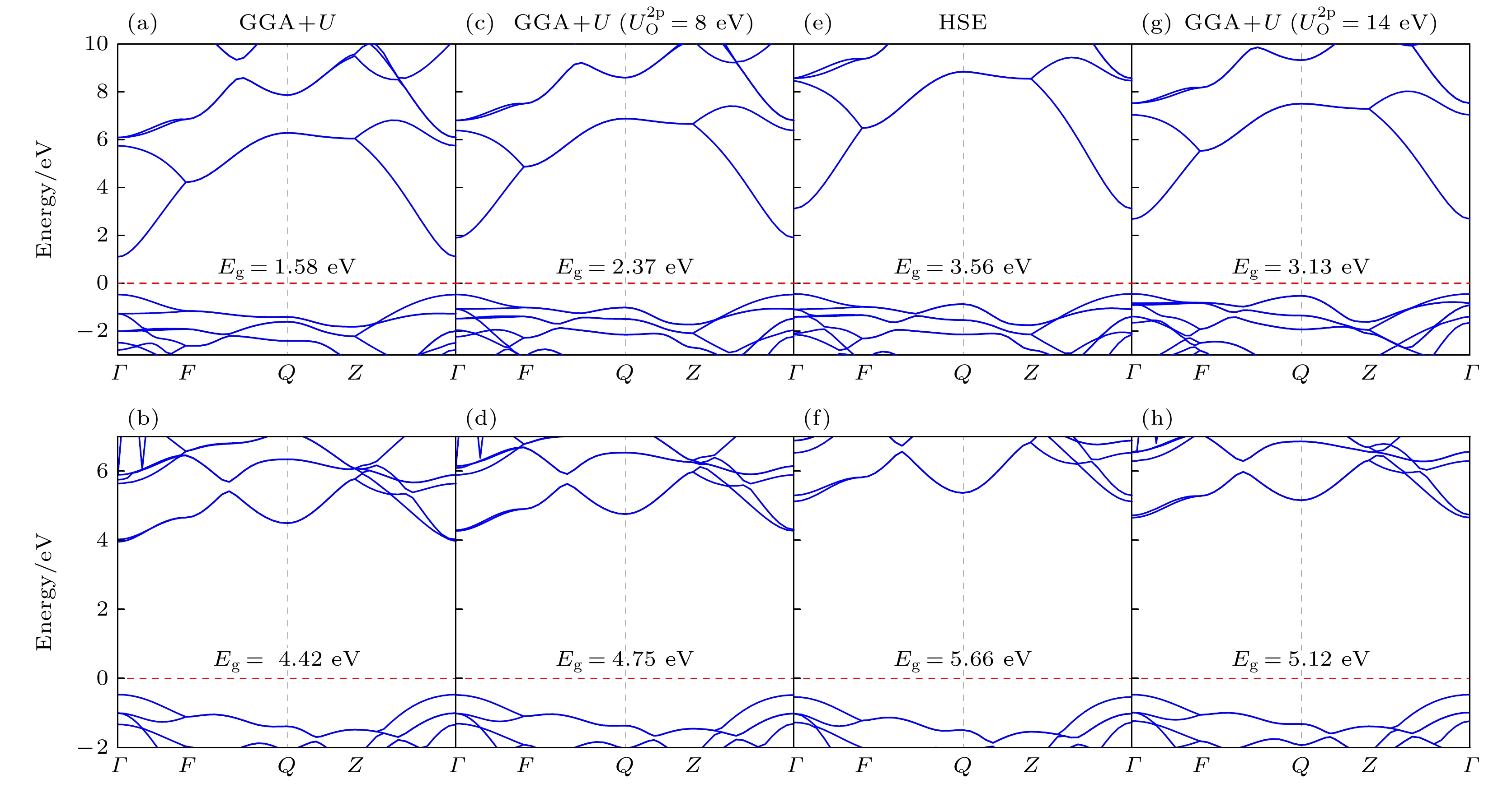
图 1 SnO2和HfO2块体的能带结构图(费米能级设为零点) (a), (b)采用GGA+U所得(a) SnO2和(b) HfO2的能带结构; (c), (d)采用$U_{\text{O}}^{{\text{2p}}}$ = 8 eV的GGA+U所得(c) SnO2和(d) HfO2的能带结构; (e), (f)采用HSE杂化泛函所得(e) SnO2和(f) HfO2的能带结构; (g), (h)采用$U_{\text{O}}^{{\text{2p}}}$ = 14 eV的GGA+U所得(g) SnO2和(h) HfO2的能带结构
Fig. 1. Band structure of bulk SnO2 and HfO2. The band structures of (a) SnO2 and (b) HfO2 obtained by GGA+U. (c) SnO2 and (d) HfO2 obtained by GGA+U with $U_{\text{O}}^{{\text{2p}}}$ = 8 eV. The band structures of (e) SnO2 and (f) HfO2 obtained by HSE hybrid functional. The band structures of (g) SnO2 and (h) HfO2 obtained by GGA+U with $U_{\text{O}}^{{\text{2p}}}$ = 14 eV. The Fermi level is set as zero.
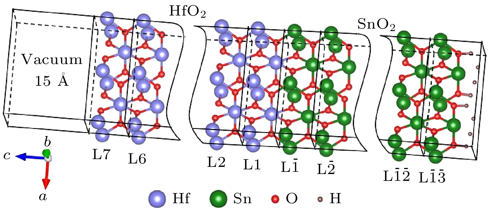
图 2 面内2×1 (HfO2)7/(SnO2)13异质结构示意图
Fig. 2. Schematic structure of the in-plane 2×1 (HfO2)7/(SnO2)13 heterostructure.
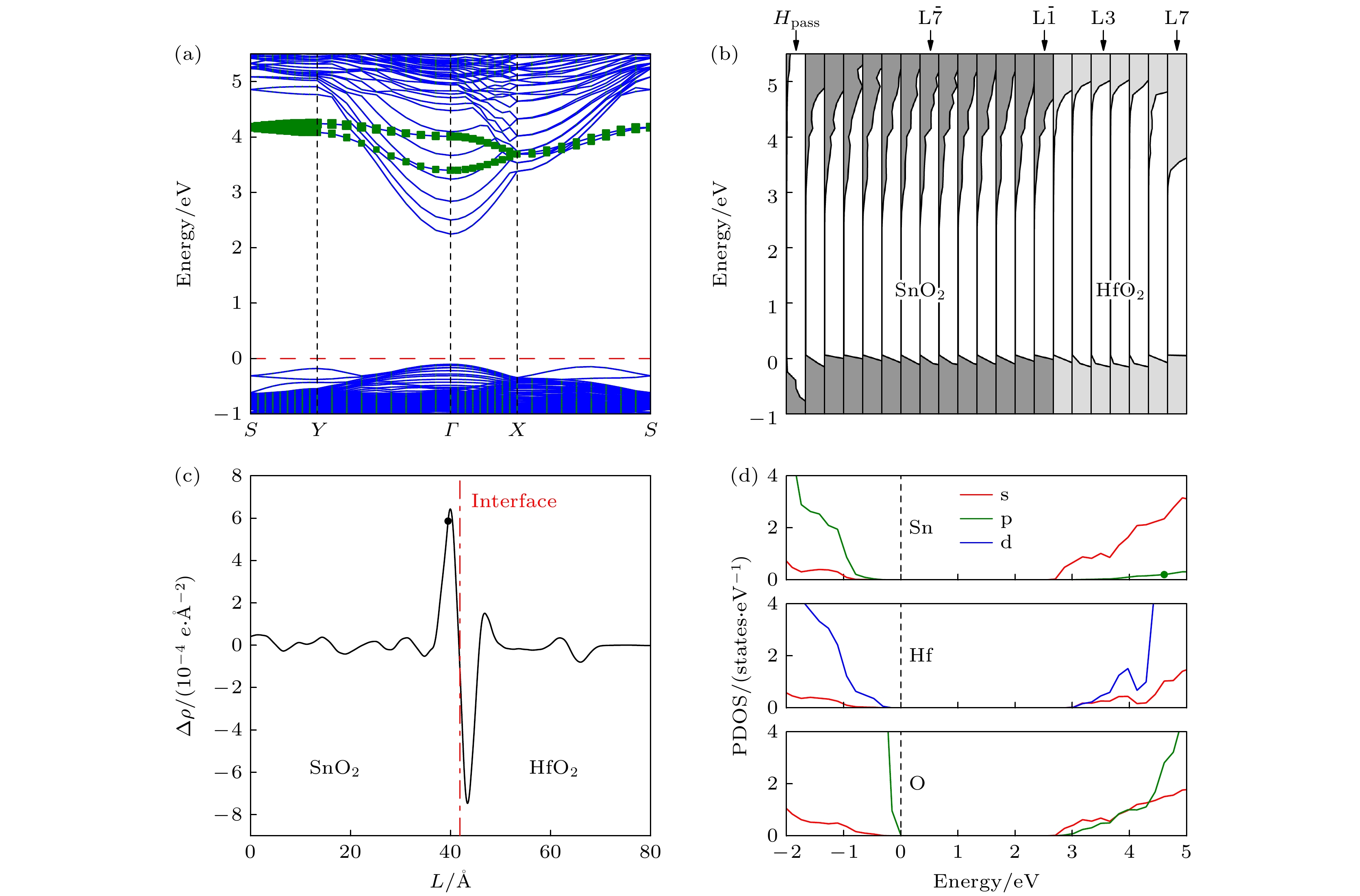
图 3 (HfO2)7/(SnO2)13异质结构的电子结构(费米能级设为零点) (a)能带结构图, 方形点线标记能带来源于异质结表面L7层不饱和悬键的畸变; (b)原子层分解态密度图; (c)平面平均电荷密度差, 其中负值和正值分别表示电子的耗尽和积累, L表示沿异质结构的距离, 点划线给出了异质结界面的位置; (d) Sn, Hf, O原子轨道投影态密度
Fig. 3. Electronic structure of (HfO2)7/(SnO2)13 heterostructure. (a) The energy band structure. The band marked by the square dots originates from the distortion of the unsaturated dangling bonds of the L7 layer near the heterojunction surface. (b) The partial density of states projected onto atomic planes. (c) The plane-averaged charge density difference. The negative and positive values represent the depletion and accumulation of electrons, respectively. L is noted as the distance along direction of the heterostructure, and the dashed line gives the location of the interface. (d) Projection density of states for Sn, Hf, and O atomic orbitals, where the Fermi level is set as zero.
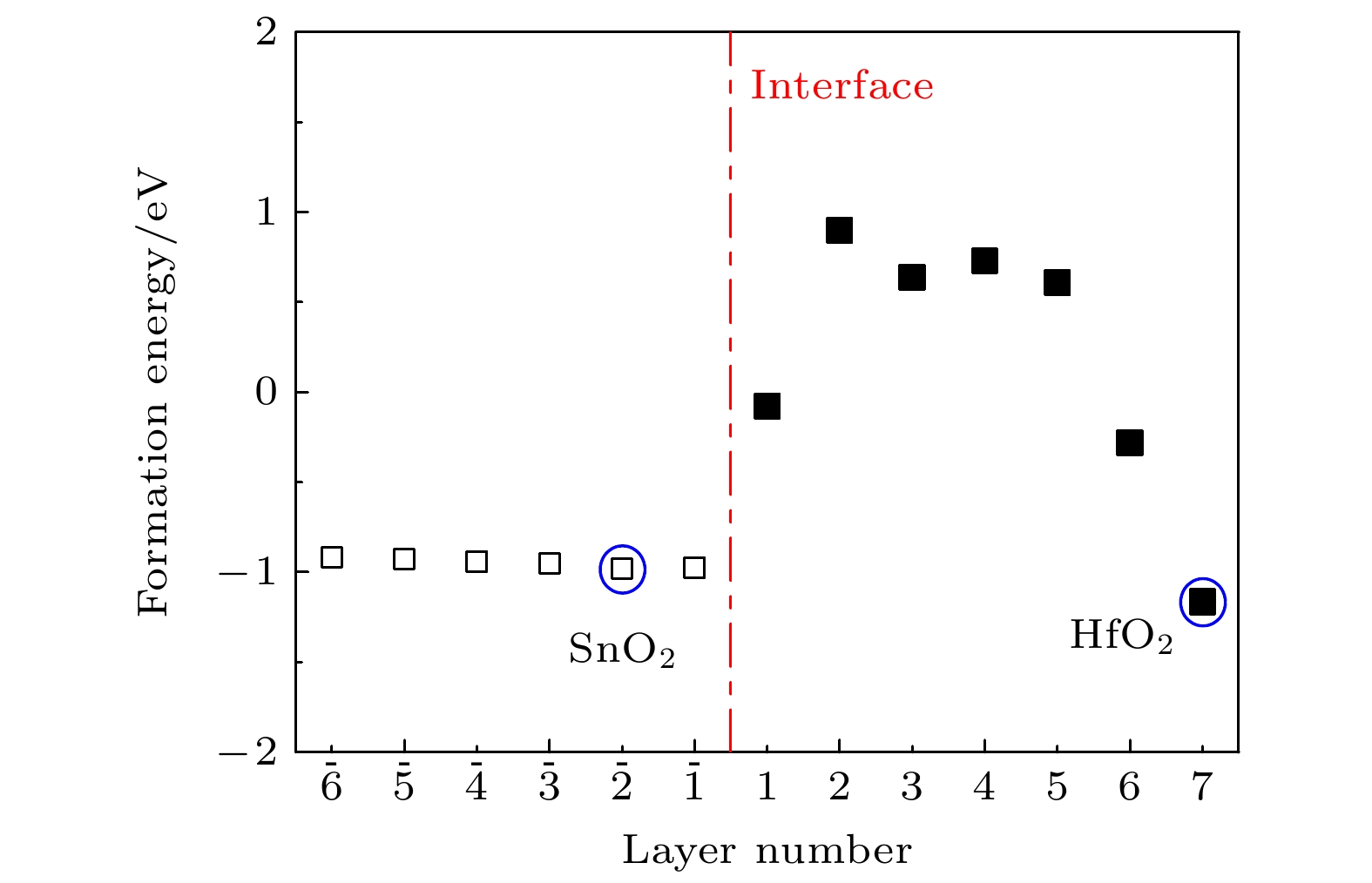
图 4 (HfO2)7/(SnO2)13异质结表面和界面附近不同原子层的氧空位形成能, 其中点划线给出了异质结界面的位置, 圆圈标记为SnO2侧和HfO2侧的氧空位形成能最低的位置
Fig. 4. Formation energies of oxygen vacancies in different atomic layers near the surface and interface of (HfO2)7/(SnO2)13 heterostructure. The dashed line gives the position of the interface of the heterostructure, and the circles mark the lowest oxygen vacancy formation energy on the SnO2 side and the HfO2 side.
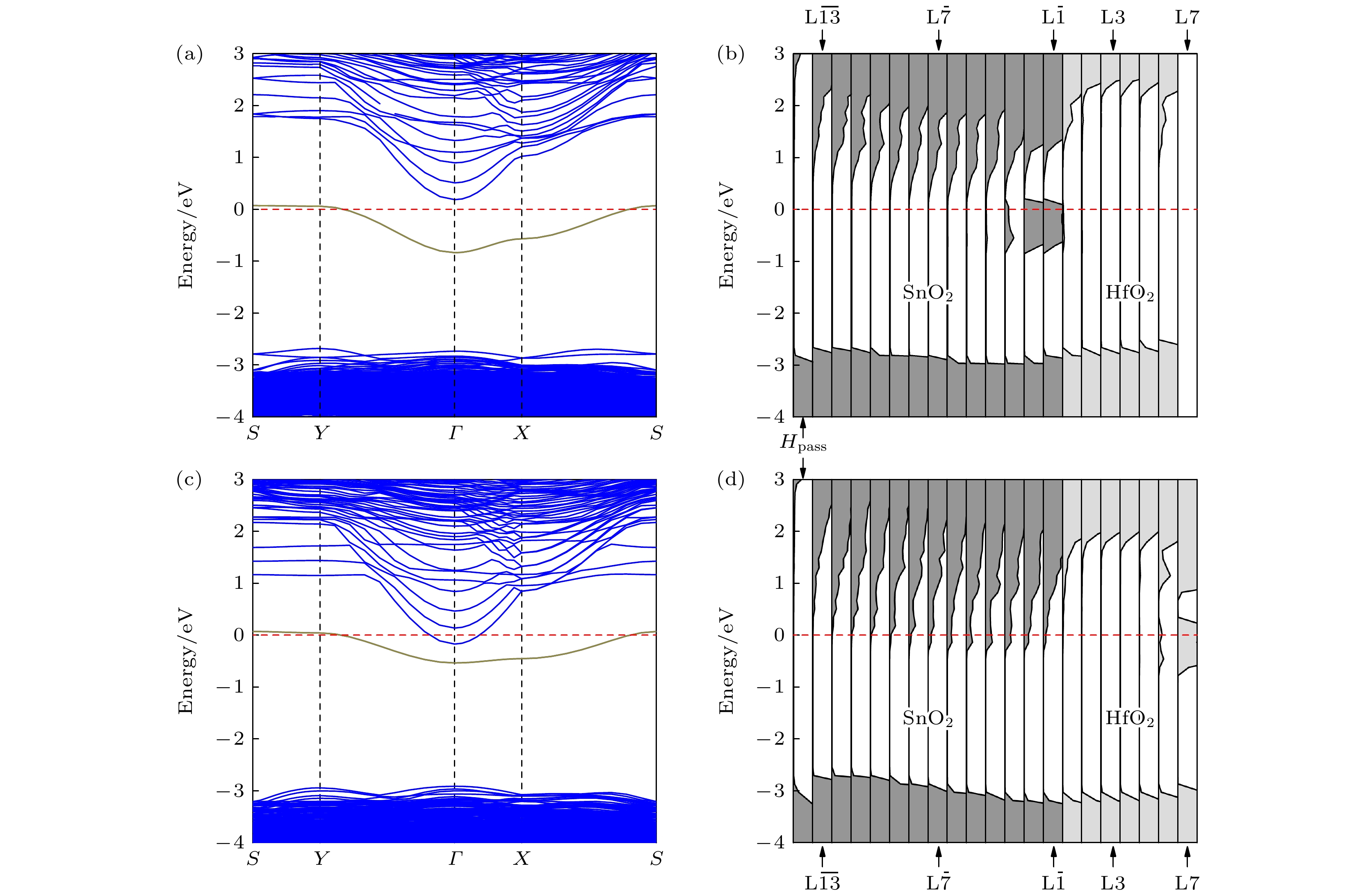
图 5 存在氧空位时(HfO2)7/(SnO2)13异质结的能带结构图和原子层分解态密度图 (a), (b)氧空位位于L$\overline {2} $原子层的情况; (c), (d)氧空位位于L7原子层的情况; 棕实线标记能带为氧空位的缺陷能级, 计算结果基于$U_{\text{O}}^{2{\text{p}}}$ = 14 eV的GGA+U方法, 费米能级设为零点
Fig. 5. Energy band structure and partial density of states projected onto atomic planes of (HfO2)7/(SnO2)13 heterostructure with oxygen vacancy: (a), (b) The cases for oxygen vacancy on the L$\overline {2} $ layer; (c), (d) the cases for oxygen vacancy on the L7 layer. The band marked by brown solid line are the defective energy levels of the oxygen vacancy. The calculation results are based on the GGA+U method of $U_{\text{O}}^{{\text{2p}}}$ = 14 eV, and the Fermi level is set as zero.
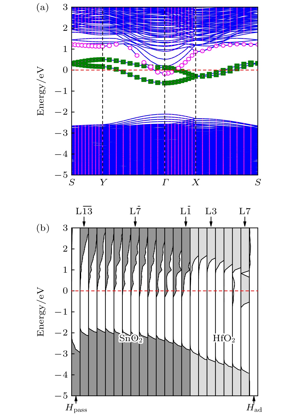
图 6 表面吸附H原子的(HfO2)7/(SnO2)13异质结的电子结构(费米能级设为零点) (a)能带结构图, 方形点线标记能带来源于表面处电子, 圆圈标记能带来自界面处电子; (b)原子层分解态密度图
Fig. 6. Electronic structure of (HfO2)7/(SnO2)13 heterostructure adsorbed H atoms on the surface. (a) The energy band structure. The band marked by the square dots originates from the surface electrons, and the band marked by the circles comes from electrons at interface. (b) The partial density of states projected onto atomic planes. The Fermi level is set as zero.
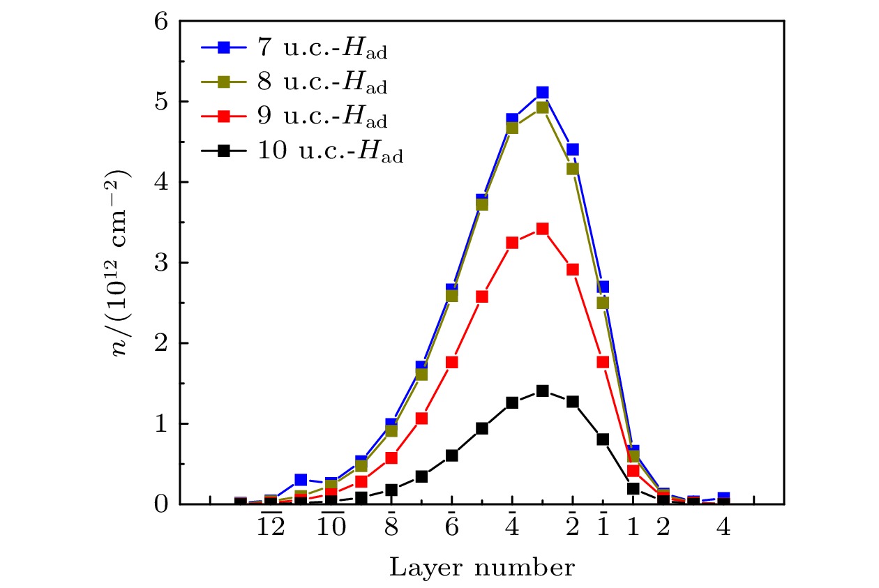
图 7 表面吸附H原子$ {\left( {{\text{Hf}}{{\text{O}}_2}} \right)_l}/{\left( {{\text{Sn}}{{\text{O}}_2}} \right)_{13}} $(l = 7, 8, 9, 10 u.c.)异质结界面附近的电子浓度
Fig. 7. Electron density near the interface of $ {\left( {{\text{Hf}}{{\text{O}}_2}} \right)_l}/ $$ {\left( {{\text{Sn}}{{\text{O}}_2}} \right)_{13}} $ (l = 7, 8, 9, 10 u.c.) heterostructures adsorbed H atoms on the HfO2 surface.
-
[1] Ohtomo A, Hwang H Y 2004 Nature 427 423
Google Scholar
[2] Tampo H, Shibata H, Matsubara K, Yamada A, Fons P, Niki S, Yamagata M, Kanie H 2006 Appl. Phys. Lett. 89 132113
Google Scholar
[3] Hotta Y, Susaki T, Hwang H Y 2007 Phys. Rev. Lett. 99 236805
Google Scholar
[4] Chen Y Z, Bovet N, Trier F, Christensen D V, Qu F M, Andersen N H, Kasama T, Zhang W, Giraud R, Dufouleur J, Jespersen T S, Sun J R, Smith A, Nygård J, Lu L, Büchner B, Shen B G, Linderoth S, Pryds N 2013 Nat. Commun. 4 1371
Google Scholar
[5] Zou K, Ismail-Beigi S, Kisslinger K, Shen X, Su D, Walker F J, Ahn C H 2015 APL Mater. 3 036104
Google Scholar
[6] Zhang Y W, Neal A, Xia Z B, Joishi C, Johnson J M, Zheng Y H, Bajaj S, Brenner M, Dorsey D, Chabak K, Jessen G, Hwang J, Mou S, Heremans J P, Rajan S 2018 Appl. Phys. Lett. 112 173502
Google Scholar
[7] 颜送灵, 唐黎明, 赵宇清 2016 65 077301
Google Scholar
Yan S L, Tang L M, Zhao Y Q 2016 Acta Phys. Sin. 65 077301
Google Scholar
[8] Zhang H R, Yun Y, Zhang X J, Zhang H, Ma Y, Yan X, Wang F, Li G, Li R, Khan T, Chen Y S, Liu W, Hu F X, Liu B G, Shen B G, Han W, Sun J R 2018 Phys. Rev. Lett. 121 116803
Google Scholar
[9] Kozuka Y, Tsukazaki A, Maryenko D, Falson J, Akasaka S, Nakahara K, Nakamura S, Awaji S, Ueno K, Kawasaki M 2011 Phys. Rev. B 84 033304
Google Scholar
[10] Chen Z, Liu Y, Zhang H, Liu Z R, Tian H, Sun Y Q, Zhang M, Zhou Y, Sun J R, Xie Y W 2021 Science 372 721
Google Scholar
[11] 王继光, 李珑玲, 邱嘉图, 陈许敏, 曹东兴 2023 72 176801
Google Scholar
Wang J G, Li L L, Qiu G T, Chen X M, Cao D X 2023 Acta Phys. Sin. 72 176801
Google Scholar
[12] Thiel S, Hammerl G, Schmehl A, Schneider C W, Mannhart J 2006 Science 313 1942
Google Scholar
[13] Chen X H, Li Z Q, Hu Z X, Gao K H 2022 Phys. Rev. B 105 205437
Google Scholar
[14] Nakano M, Tsukazaki A, Ueno K, Gunji R Y, Ohtomo A, Fukumura T, Kawasaki M 2010 Appl. Phys. Lett. 96 052116
Google Scholar
[15] 张阳, 顾书林, 叶建东, 黄时敏, 顾然, 陈斌, 朱顺明, 郑有炓 2013 62 150202
Google Scholar
Zhang Y, Gu S L, Ye J D, Huang S M, Gu R, Chen B, Zhu S M, Zhen Y D 2013 Acta Phys. Sin. 62 150202
Google Scholar
[16] Himmetoglu B, Janotti A, Peelaers H, Alkauskas A, Van de Walle C G 2014 Phys. Rev. B 90 241204
Google Scholar
[17] Himmetoglu B, Janotti A 2016 J. Phys. Condens. Matter 28 065502
Google Scholar
[18] Lee J, Demkov A A 2008 Phys. Rev. B 78 193104
Google Scholar
[19] Chen X H, Li Z Q, Hou D Y, Hu Z X, Gao K H 2023 Phys. Rev. B 107 165411
Google Scholar
[20] Sanon G, Rup R, Mansingh A 1991 Phys. Rev. B 44 5672
Google Scholar
[21] Toyosaki H, Kawasaki M, Tokura Y 2008 Appl. Phys. Lett. 93 132109
Google Scholar
[22] Paudel T R, Tsymbal E Y 2017 Phys. Rev. B 96 245423
Google Scholar
[23] Nazir S, Cheng J L, Yang K S 2016 ACS Appl. Mater. Interfaces 8 390
Google Scholar
[24] Lee B H, Kang L, Nieh R, Qi W J, Lee J C 2000 Appl. Phys. Lett. 76 1926
Google Scholar
[25] Seo M, Kim S K, Han J H, Hwang C S 2010 Chem. Mater. 22 4419
Google Scholar
[26] Seo M, Kim S K, Min Y S, Hwang C S 2011 J. Mater. Chem. 21 18497
Google Scholar
[27] Blöchl P E 1994 Phys. Rev. B 50 17953
Google Scholar
[28] Kresse G, Hafner J 1993 Phys. Rev. B 47 558
Google Scholar
[29] Kresse G, Furthmüller J 1996 Phys. Rev. B 54 11169
Google Scholar
[30] Kresse G, Joubert D 1999 Phys. Rev. B 59 1758
Google Scholar
[31] Gilani R, Rehman S U, Butt F K, Haq B U, Aleem F 2018 Silicon 10 2317
Google Scholar
[32] Singh A K, Janotti A, Schefler M, Van de Walle C G 2008 Phys. Rev. Lett. 101 055502
Google Scholar
[33] Park J, Saidi W A, Chorpening B, Duan Y H 2021 J. Phys. Chem. C 125 22231
Google Scholar
[34] Marcillo F, Stashans A 2015 J. Theor. Comput. Chem. 13 1450069
Google Scholar
[35] Heyd J, Peralta J E, Scuseria G E, Martin R L 2005 J. Chem. Phys. 123 174101
Google Scholar
[36] Pavoni E, Mohebbi E, Stipa P, Mencarelli D, Pierantoni L 2022 Materials 15 4175
Google Scholar
[37] Akbar W, Elahi I, Nazir S 2020 J. Magn. Magn. Mater. 511 166948
Google Scholar
[38] Li J P, Meng S H, Yang C, Lu H T, Tohyama T 2018 Chin. Phys. B 27 027101
Google Scholar
[39] Krishnaswamy K, Himmetoglu B, Kang Y, Janotti A, Van de Walle C G 2017 Phys. Rev. B 95 205202
Google Scholar
[40] Herranz G, Basletić M, Bibes M, Carrétéro C, Tafra E, Jacquet E, Bouzehouane K, Deranlot C, HamzićA, Broto J M, Barthélémy A, Fert A 2007 Phys. Rev. Lett. 98 216803
Google Scholar
[41] Oh T 2017 Trans. Electr. Electron. Mater. 18 21
Google Scholar
[42] Liu H Y, Zeng F, Lin Y S, Wang G Y, Pan F 2013 Appl. Phys. Lett. 102 181908
Google Scholar
[43] Singh R, Khan M A, Mukherjee S, Kranti A 2018 IEEE Trans. Electron Devices 65 2850
Google Scholar
[44] Bandura A V, Kubicki J D, Sofo J O 2008 J. Phys. Chem. B 112 11616
Google Scholar
[45] Li L, Huang X, Zhang Y F, Guo X, Chen W K 2013 Appl. Surf. Sci. 264 424
Google Scholar
[46] Jia H, Liang W H, Zhou M, Cao E S, Yang Z, Hao W T, Zhang Y J 2018 J. Supercond. Novel. Magn. 31 3361
Google Scholar
[47] Li Y, Phattalung S N, Limpijumnong S, Kim J, Yu J 2011 Phys. Rev. B 84 245307
Google Scholar


 下载:
下载:


计量
- 文章访问数: 1070
- PDF下载量: 35
- 被引次数: 0
