-
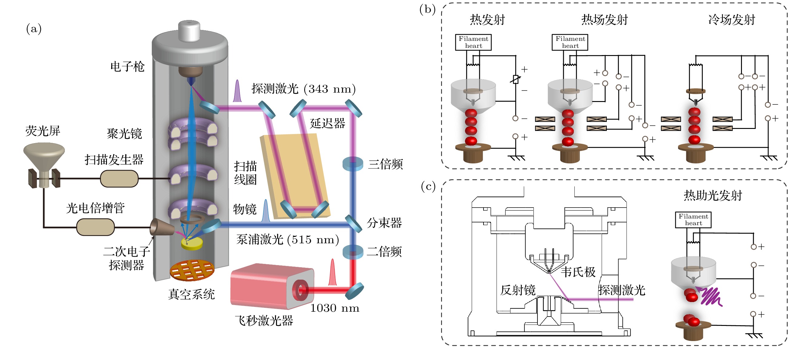
超快扫描电子显微镜将泵浦探测技术与显微成像相结合, 能够实现高时空分辨率下光诱导表面电荷动力学的可视化研究, 对于半导体表面态以及光电器件的高分辨检测具有非常重要的意义. 本文基于首台全国产化超快扫描电子显微镜的研制工作, 阐述了将热发射电子枪改造成光发射电子枪后的参数化设计, 定量分析了偏压, 阴极、韦氏极、阳极的空间位置与交叉点位置、大小、发散角的依赖关系. 分析结果显示, 当韦氏极与阳极位置从8 mm调整到23 mm后, 通过将灯丝深度从0.65 mm调整至0.45 mm, 配合偏压调节可以实现热发射高分辨成像、低工作电压以及光发射的正常使用. 此外, 也分析了反射镜分布对电子光路的影响, 发现当阳极高出反射镜1.4 mm后, 图像畸变几乎消失. 还研究了偏置电压对脉冲光电子在时域上的影响, 结果表明随着偏压的增大, 光发射的时间零点会推后且时间展宽变大. 这些工作将为后续超快电子显微镜的发展及光发射电子源的设计奠定基础.Ultrafast scanning electron microscope (USEM) integrates pump-probe technique with microscopic imaging, enabling the visualizing of photon-induced surface charge dynamics with high spatial and temporal resolution. This capability is crucial for high-resolution detection of semiconductor surface states and optoelectronic devices. This work discusses the parametric design of a thermionic emission electron gun that has been modified into a photoemission electron gun, based on a home-built ultrafast scanning electron microscope. Given that the dose of the photoemitting electron beam is usually much lower than that of thermionic emission, the transition to photoemission requires the removal of the self-bias voltage function of the original electron microscope power supply to ensure the normal operation of the Wehnelt electrode. We quantitatively analyze the dependence of bias voltage, cathode, Wehnelt electrode, and anode on the position, size and divergence angle of crossover, which helps to improve the parameter adjustment of the modified electron gun. The analysis results indicate that if the distance between the Wehnelt electrode and the anode is adjusted from 8 to 23 mm, the distance between the filament and wehnelt can be changes from 0.65 to 0.45 mm to cooperate with the bias adjustment, so that the normal use of high-resolution thermionic emission mode, low voltage mode and photoemission mode can be realized. Subsequently, the effect of the mirror’s position on the electron optical path is analyzed. It is found that when the anode is raised 1.4 mm above the mirror, the influence on the electron optical path can be ignored. Additionally, the zero-of-time and temporal broadening of the photo-electron pulse are further simulated. The results indicate that with the increase of bias voltage, the time zero of photoemission will be delayed and the temporal broadening will become larger. This study lays a foundation for the future development of ultrafast electron microscope and the design of photoemission electron sources.
-
Keywords:
- photo-emission electron gun /
- ultrafast scanning electron microscope /
- electron optics /
- finite element analysis methods
[1] Mohammed O F, Yang D S, Pal S K, Zewail A H 2011 J. Am. Chem. Soc. 133 7708
 Google Scholar
[2] Yang D S, Mohammed O F, Zewail A H 2010 Proc. Natl. Acad. Sci. U.S.A. 107 14993
 Google Scholar
[3] Zhang Y, Chen X, Yu Y, Huang Y, Qiu M, Liu F, Feng M, Gao C, Deng S, Fu X 2024 Adv. Sci. 11 2400633
 Google Scholar
[4] Perez C, Ellis S R, Alcorn F M, Smoll E J, Fuller E J, Leonard F, Chandler D, Talin A A, Bisht R S, Ramanathan S, Goodson K E, Kumar S 2024 Sci. Adv. 10 eadn8980
 Google Scholar
[5] Tian Y, Yang D, Ma Y, Li Z, Li J, Deng Z, Tian H, Yang H, Sun S, Li J 2024 Nanomaterials 14 310
 Google Scholar
[6] Najafi E, Ivanov V, Zewail A, Bernardi M 2017 Nat. Commun. 8 15177
 Google Scholar
[7] Najafi E, Scarborough T D, Tang J, Zewail A 2015 Science 347 164
 Google Scholar
[8] Ellis S R, Bartelt N C, Leonard F, Celio K C, Fuller E J, Hughart D R, Garland D, Marinella M J, Michael J R, Chandler D W, Liao B, Talin A A 2021 Phys. Rev. B 104 L161303
 Google Scholar
[9] Pan J H, Liu S, Tang J 2021 Phys. Rev. B 104 045309
 Google Scholar
[10] Liao B, Najafi E, Li H, Minnich A J, Zewail A H 2017 Nat. Nanotechnol. 12 871
 Google Scholar
[11] Liao B, Zhao H, Najafi E, Yan X, Tian H, Tice J, Minnich A J, Wang H, Zewail A H 2017 Nano Lett. 17 3675
 Google Scholar
[12] Bose R, Adhikari A, Burlakov V M, Liu G Y, Haque M A, Priante D, Hedhili M N, Wehbe N, Zhao C, Yang H Z, Ng T K, Goriely A, Bakr O M, Wu T, Ooi B S, Mohammed O F 2018 ACS Energy Lett. 3 476
 Google Scholar
[13] Shaheen B S, El-Zohry A M, Yin J, De Bastiani M, De Wolf S, Bakr O M, Mohammed O F 2019 J. Phys. Chem. Lett. 10 1960
 Google Scholar
[14] Shaheen B S, El-Zohry A M, Zhao J, Yin J, Hedhili M N, Bakr O M, Mohammed O F 2020 ACS Appl. Mater. Interfaces 12 7760
 Google Scholar
[15] Sun J, Adhikari A, Shaheen B S, Yang H, Mohammed O F 2016 J. Phys. Chem. Lett. 7 985
 Google Scholar
[16] Najafi E, Liao B, Scarborough T, Zewail A 2018 Ultramicroscopy 184 46
 Google Scholar
[17] Kozak M, McNeur J, Schonenberger N, Illmer J, Li A, Tafel A, Yousefi P, Eckstein T, Hommelhoff P 2018 J. Appl. Phys. 124 023104
 Google Scholar
[18] Shiloh R, Chlouba T, Hommelhoff P 2022 Phys. Rev. Lett. 128 235301
 Google Scholar
[19] Arashida Y, Jeong S, Kawasaki K, Emoto Y, Noyama G, Hada M, Kishibe Y, Shigekawa H, Akada K, Yoshida S, Fujita J ichi 2024 ACS Photonics 11 2171
 Google Scholar
[20] Haine M E, Cosslett V E, Marton L 1961 Phys. Today 14 52
 Google Scholar
[21] Bigelow W C 2010 Microsc. Today 18 26
 Google Scholar
-
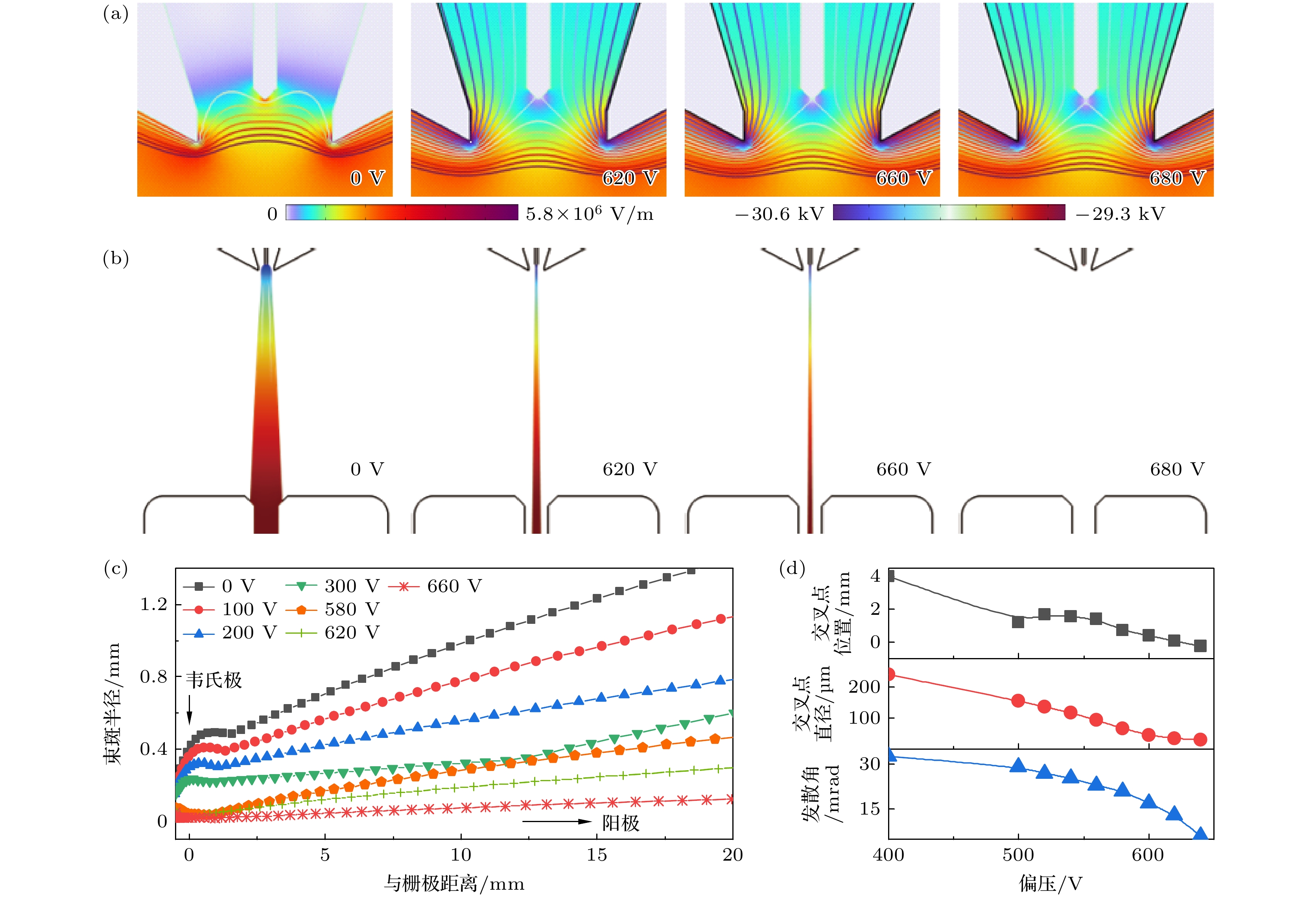
图 2 偏压对电子光学的影响 (a) 灯丝尖端的电场分布; (b) 电子束轨迹; (c) 电子束的几何光学, 其中z = 0 mm处为韦氏极, z = –0.5 mm处为灯丝尖端, z = 23 mm处为阳极; (d) 交叉点位置、直径、发散角
Fig. 2. Effect of bias voltage on the electron optics: (a) Electric field distribution at the filament tip; (b) electron beam trajectories; (c) optics geometry of electron beam, where the wehnelt at z = 0 mm, the filament tip at z = –0.5 mm, and the anode at z = 23 mm; (d) position, diameter, divergence angle as a function of bias voltage.
图 3 (a)截止偏压与韦氏极-阳极间距的关系, 工作电压为30 kV; (b)截止偏压与工作电压的关系, 韦氏极与阳极间距为23 mm
Fig. 3. (a) Relationship between cutoff bias voltage and the distance between the wehnelt electrode and the anode at 30 kV; (b) relationship between cutoff bias voltage and working voltage with a distance of 23 mm between the wehnelt electrode and the anode.
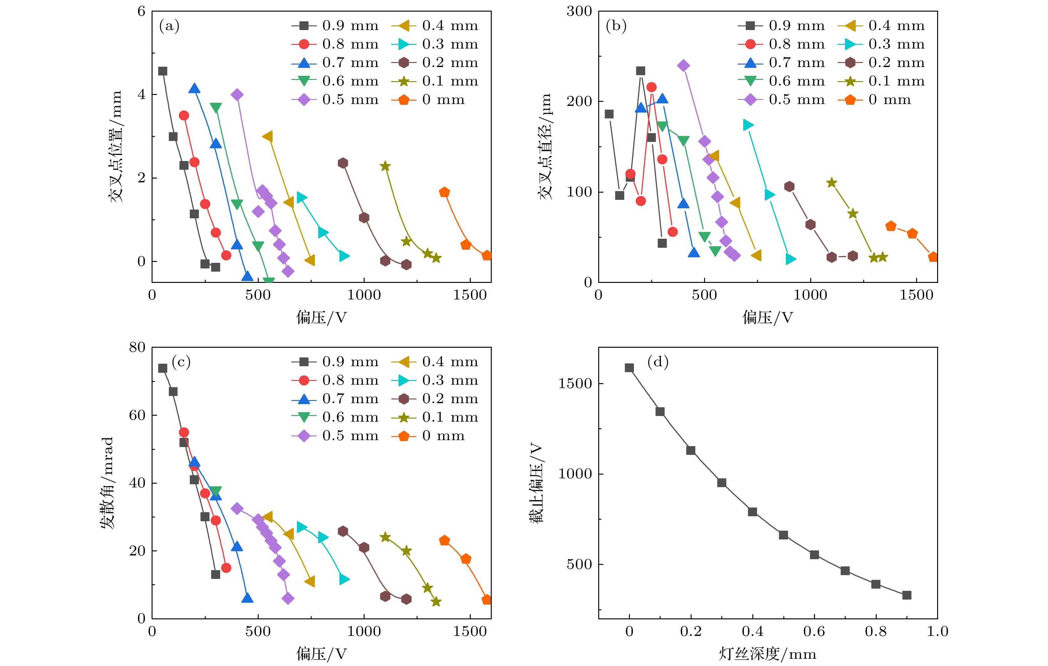
图 4 不同灯丝深度的发射状态 (a)—(c) 不同灯丝深度的交叉点位置、交叉点大小、发散角等随偏压的变化; (d) 不同灯丝深度条件下的截止偏压, 当偏压大于截止偏压时处于禁止发射状态
Fig. 4. Emission states at different distances between filament and wehnelt: (a)–(c) Variation of positions, diameters and divergence angles of crossover with bias voltage; (d) the cut-off bias voltage at the different distance between filament and wehnelt; when the bias voltage is greater than the cut-off bias voltage, the emission is prohibited.
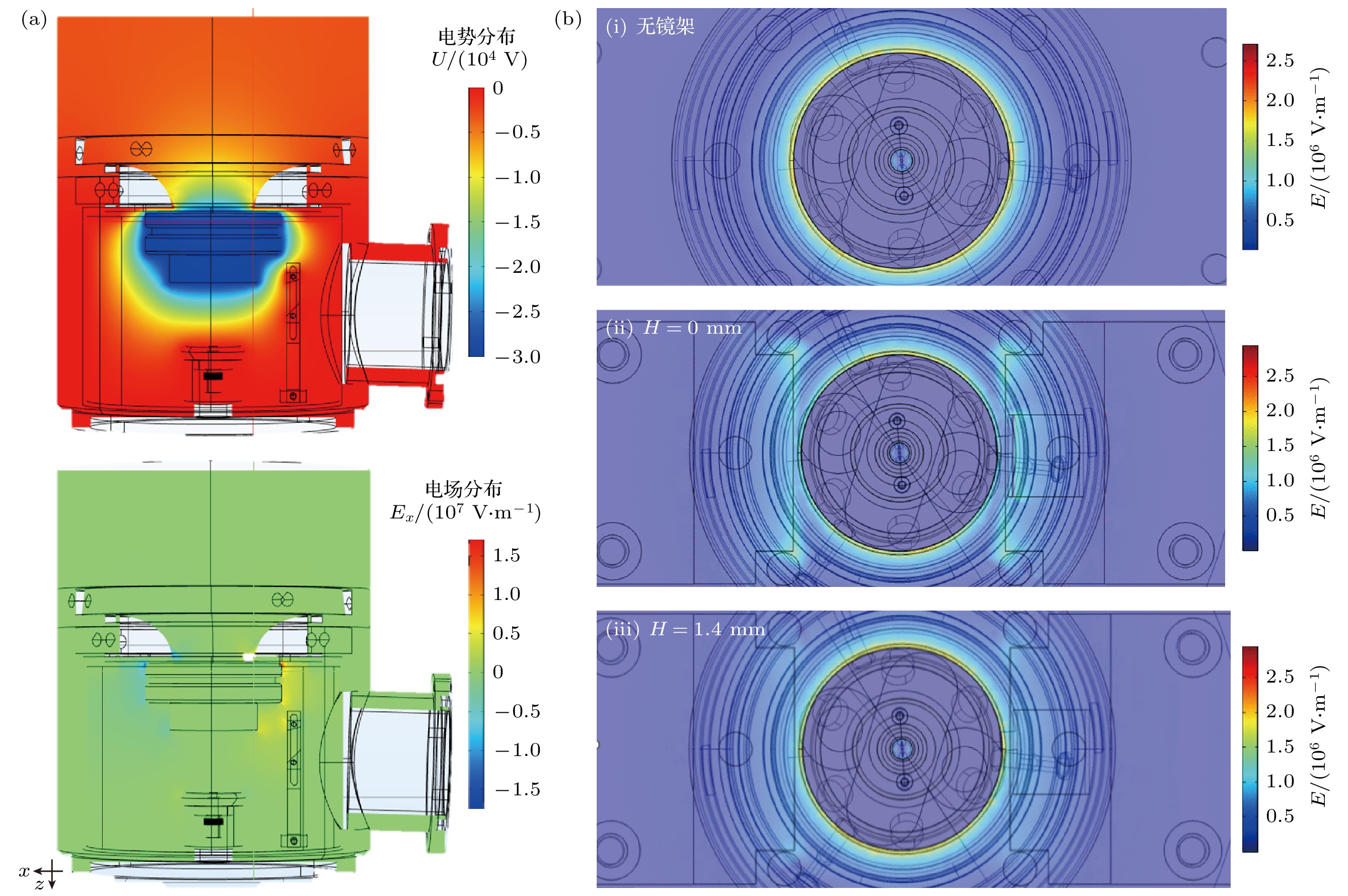
图 5 反射镜对电子枪内部电场的影响 (a) 不对称放置反射镜的纵向截面电势分布(上图)、电场分布(下图). (b) 阳极平面处的横向截面电场分布 (i)无反射镜; (ii), (iii)阳极与反射镜高度差为H = 0, 1.4 mm
Fig. 5. Effect of mirrors on the electric field inside the electron gun: (a) Longitudinal cross-sectional potential distribution (top) and electric field distribution (bottom) for asymmetrically placed mirrors. (b) Transverse cross-sectional electric field distribution at the anode plane: (i) Without mirrors; (ii), (iii) height difference between the anode and mirror H = 0, 1.4 mm.
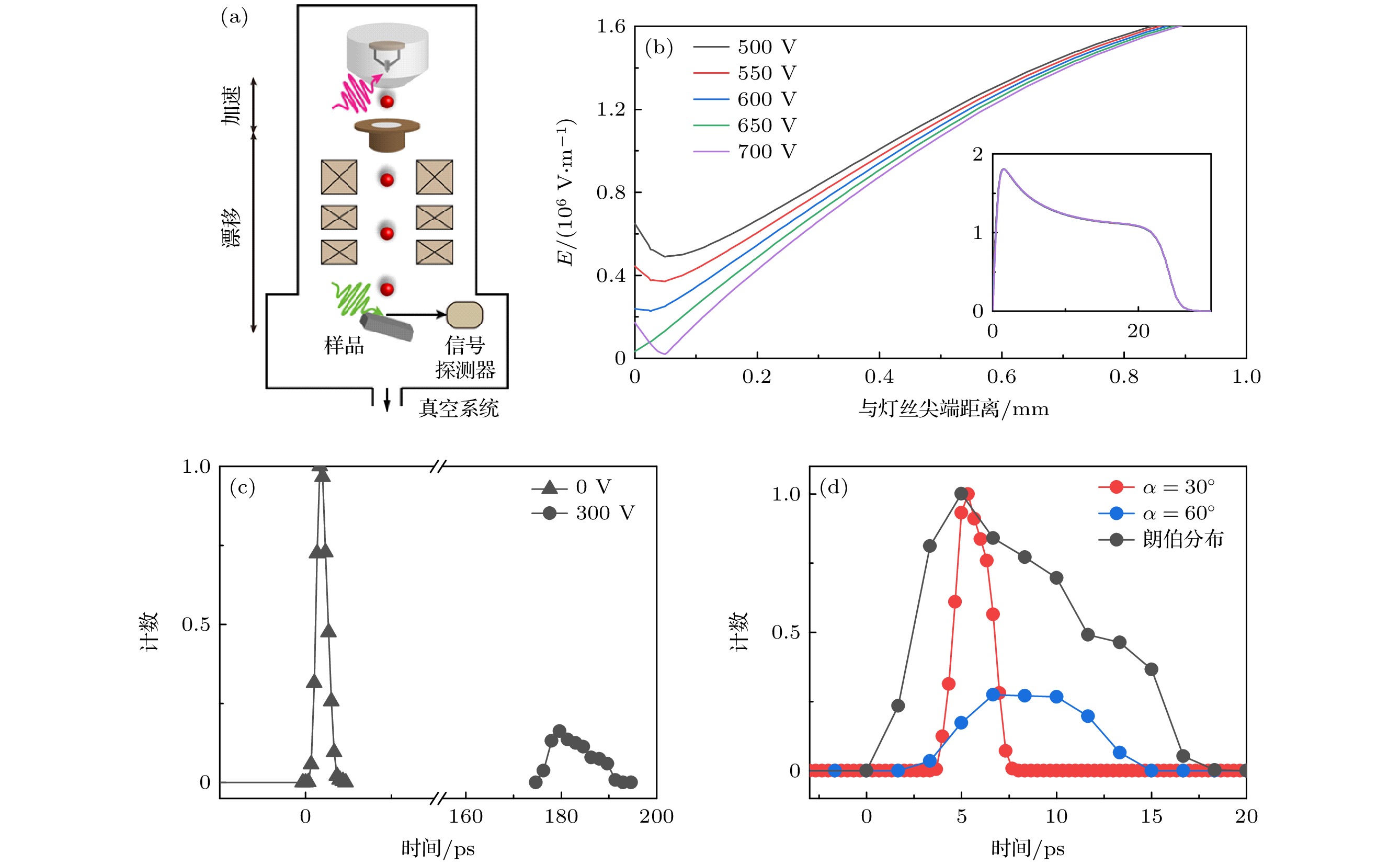
图 6 偏压对电子漂移时间的影响 (a) 电子漂移示意图; (b) 阴极附近光轴上的电场分布随偏压的变化, 插图为整个加速区间电场分布; (c) 偏压Vbias = 0, 300 V时的电子束时间展宽; (d) 偏压为300 V时, 不同发射分布下的电子束时间展宽
Fig. 6. Effect of bias voltages on electron drift time: (a) Schematic diagram of electron drift; (b) electric field distribution along the optical axis near the cathode as a function of bias voltage, with the illustration showing the electric field distribution across the entire acceleration region; (c) temporal broadening of the electron beam at Vbias = 0, 300 V; (d) temporal broadening of the electron beam under different emission distributions at Vbias = 300 V.
-
[1] Mohammed O F, Yang D S, Pal S K, Zewail A H 2011 J. Am. Chem. Soc. 133 7708
 Google Scholar
[2] Yang D S, Mohammed O F, Zewail A H 2010 Proc. Natl. Acad. Sci. U.S.A. 107 14993
 Google Scholar
[3] Zhang Y, Chen X, Yu Y, Huang Y, Qiu M, Liu F, Feng M, Gao C, Deng S, Fu X 2024 Adv. Sci. 11 2400633
 Google Scholar
[4] Perez C, Ellis S R, Alcorn F M, Smoll E J, Fuller E J, Leonard F, Chandler D, Talin A A, Bisht R S, Ramanathan S, Goodson K E, Kumar S 2024 Sci. Adv. 10 eadn8980
 Google Scholar
[5] Tian Y, Yang D, Ma Y, Li Z, Li J, Deng Z, Tian H, Yang H, Sun S, Li J 2024 Nanomaterials 14 310
 Google Scholar
[6] Najafi E, Ivanov V, Zewail A, Bernardi M 2017 Nat. Commun. 8 15177
 Google Scholar
[7] Najafi E, Scarborough T D, Tang J, Zewail A 2015 Science 347 164
 Google Scholar
[8] Ellis S R, Bartelt N C, Leonard F, Celio K C, Fuller E J, Hughart D R, Garland D, Marinella M J, Michael J R, Chandler D W, Liao B, Talin A A 2021 Phys. Rev. B 104 L161303
 Google Scholar
[9] Pan J H, Liu S, Tang J 2021 Phys. Rev. B 104 045309
 Google Scholar
[10] Liao B, Najafi E, Li H, Minnich A J, Zewail A H 2017 Nat. Nanotechnol. 12 871
 Google Scholar
[11] Liao B, Zhao H, Najafi E, Yan X, Tian H, Tice J, Minnich A J, Wang H, Zewail A H 2017 Nano Lett. 17 3675
 Google Scholar
[12] Bose R, Adhikari A, Burlakov V M, Liu G Y, Haque M A, Priante D, Hedhili M N, Wehbe N, Zhao C, Yang H Z, Ng T K, Goriely A, Bakr O M, Wu T, Ooi B S, Mohammed O F 2018 ACS Energy Lett. 3 476
 Google Scholar
[13] Shaheen B S, El-Zohry A M, Yin J, De Bastiani M, De Wolf S, Bakr O M, Mohammed O F 2019 J. Phys. Chem. Lett. 10 1960
 Google Scholar
[14] Shaheen B S, El-Zohry A M, Zhao J, Yin J, Hedhili M N, Bakr O M, Mohammed O F 2020 ACS Appl. Mater. Interfaces 12 7760
 Google Scholar
[15] Sun J, Adhikari A, Shaheen B S, Yang H, Mohammed O F 2016 J. Phys. Chem. Lett. 7 985
 Google Scholar
[16] Najafi E, Liao B, Scarborough T, Zewail A 2018 Ultramicroscopy 184 46
 Google Scholar
[17] Kozak M, McNeur J, Schonenberger N, Illmer J, Li A, Tafel A, Yousefi P, Eckstein T, Hommelhoff P 2018 J. Appl. Phys. 124 023104
 Google Scholar
[18] Shiloh R, Chlouba T, Hommelhoff P 2022 Phys. Rev. Lett. 128 235301
 Google Scholar
[19] Arashida Y, Jeong S, Kawasaki K, Emoto Y, Noyama G, Hada M, Kishibe Y, Shigekawa H, Akada K, Yoshida S, Fujita J ichi 2024 ACS Photonics 11 2171
 Google Scholar
[20] Haine M E, Cosslett V E, Marton L 1961 Phys. Today 14 52
 Google Scholar
[21] Bigelow W C 2010 Microsc. Today 18 26
 Google Scholar
计量
- 文章访问数: 4084
- PDF下载量: 235
- 被引次数: 0


 下载:
下载:
