


-
非晶氧化镓(a-GaOx)具有较宽的带隙、大击穿场强、高可见光透过率、对特定波长的紫外光敏感、制备温度低、工艺较为简单、衬底适用范围广及易获得高质量薄膜等特点, 一般用于制备透明电子器件、紫外探测器, 大功率器件以及气体传感器. 目前对于a-GaOx的研究较少且集中于氧镓化学计量比(O/Ga比)小于等于1.5的薄膜. 薄膜中的O/Ga比的变化会影响其化学键的形成, 并对能带结构产生较大影响, 本文通过控制合适的工艺参数, 制备了氧镓比从3.89—3.39呈梯度变化的薄膜, 并对其能带结构和MS界面电子输运机制进行研究, 发现其光学带隙和局域态浓度逐渐增大, 其MS界面IV特性从肖特基整流特性逐渐向欧姆特性转变. 结果表明, 氧原子比例增大会使其价带顶升高, 并且过量的氧原子会与镓原子形成Ga2O, 使其局域态浓度增大, 导致其导带底降低以及施主浓度增大, 从而改变MS界面的电子输运机制.Amorphous gallium oxide (a-GaOx) exhibits excellent electrical conductivity, a wide bandgap, high breakdown field strength, high visible light transmittance, high sensitivity to specific ultraviolet wavelengths, low preparation temperatures, relatively simple processing, wide substrate applicability, and ease of obtaining high-quality thin films. These attributes make it a suitable candidate for applications in transparent electronic devices, ultraviolet detectors, high-power devices, and gas sensors. Presently, the research on a-GaOx remains limited, focusing primarily on films with an O/Ga ratio less than or equal to 1.5. Increasing the concentration of oxygen vacancies to enhance the conductivity of the material often leads to a reduction in its bandgap, which is undesirable for high-power applications. Variations in O/Ga in the films can affect the formation of chemical bonds and significantly influence the band structure. In this study, five groups of a-GaOx thin films with high oxygen-to-gallium ratios are successfully fabricated by increasing the gas flow rate at low sputtering power. The elemental compositions of the films are analyzed using energy dispersive spectroscopy (EDS), revealing the O/Ga ratio gradually decreasing from 3.89 to 3.39. Phase analysis by using X-ray Diffraction (XRD) confirms the amorphous nature of the films. Optical properties are characterized using an ultraviolet-visible spectrophotometer (UV-Vis), indicating that the optical bandgap and the density of localized states gradually increase. X-ray photoelectron spectroscopy (XPS) is utilized to analyze the elemental compositions, chemical states, and valence band structures of the films, showing that the valence band maximum decreases and the content of Ga2O within the material increases. Subsequently, Au/a-Ga2Ox/Ti/Au Schottky devices are fabricated under the same processing conditions. The I-V characteristics of these devices are measured using a Keithley 4200, revealing changes in the electron transport mechanism at the metal-semiconductor (MS) interface, with the gradual increase in electron affinity calculated. C-V characteristics are measured using a Keithley 590, and the donor concentration (density of localized states) at the interface is calculated to gradually increase. In summary, by controlling appropriate process parameters, it is possible to improve the conductivity of electronic devices while increasing the bandgap of a-GaOx, which is significant for high-power applications.
-
Keywords:
- amorphous gallium oxide /
- O/Ga ratio /
- band structure /
- electron transport mechanism
-
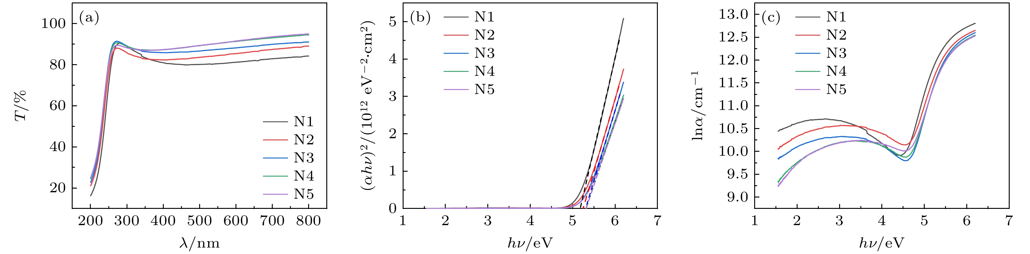
图 2 (a) a-GaOx薄膜的紫外-可见光吸收率曲线; (b) a-GaOx薄膜的$ hv{\text{ - }}{\left( {\alpha hv} \right)^2} $关系曲线; (c) a-GaOx薄膜的$ \ln \alpha {\text{ - }}hv $关系曲线
Fig. 2. (a) Ultraviolet-visible light absorption curve of a-GaOx thin film; (b) the $ hv{\text{ - }}{\left( {\alpha hv} \right)^2} $ relationship curve of a-GaOx thin film; (c) the $ \ln \alpha {\text{ - }}hv $ relationship curve of a-GaOx thin film.
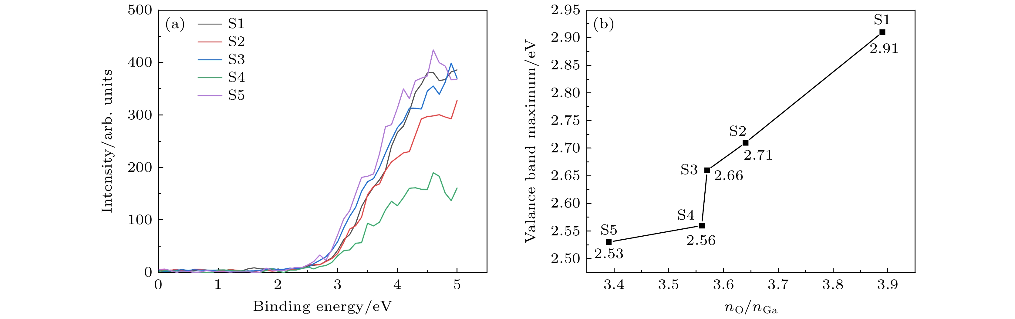
图 3 (a) a-GaOx薄膜的XPS价带谱; (b) a-GaOx薄膜的价带顶能量值
Fig. 3. (a) XPS valence band spectrum of a-GaOx thin films; (b) the valence of a-GaOx film with the maximum energy value.
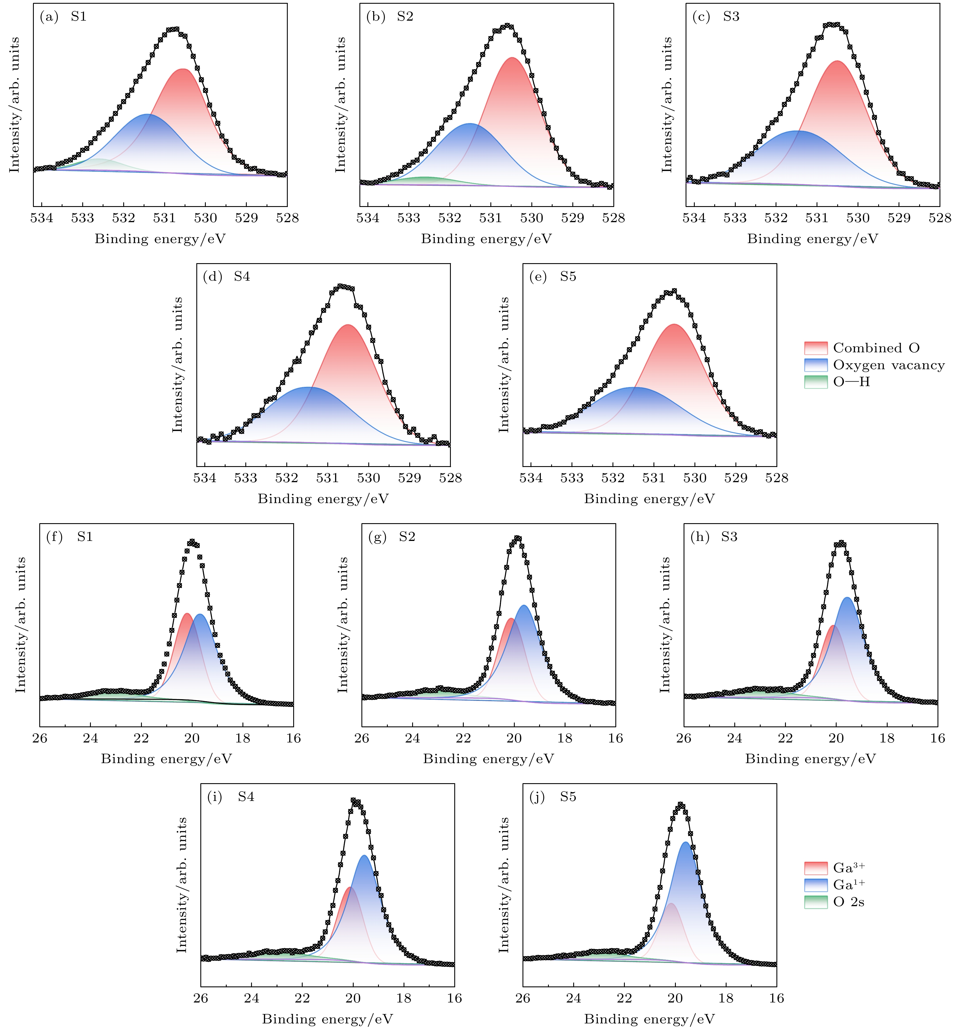
图 4 (a)—(e) a-GaOx薄膜O 1s的XPS图谱; (f)—(j) a-GaOx薄膜Ga 3d XPS图谱
Fig. 4. (a)–(e) O 1s XPS spectra of a-GaOx thin film; (f)–(j) Ga 3d XPS spectra of a-GaOx thin film.
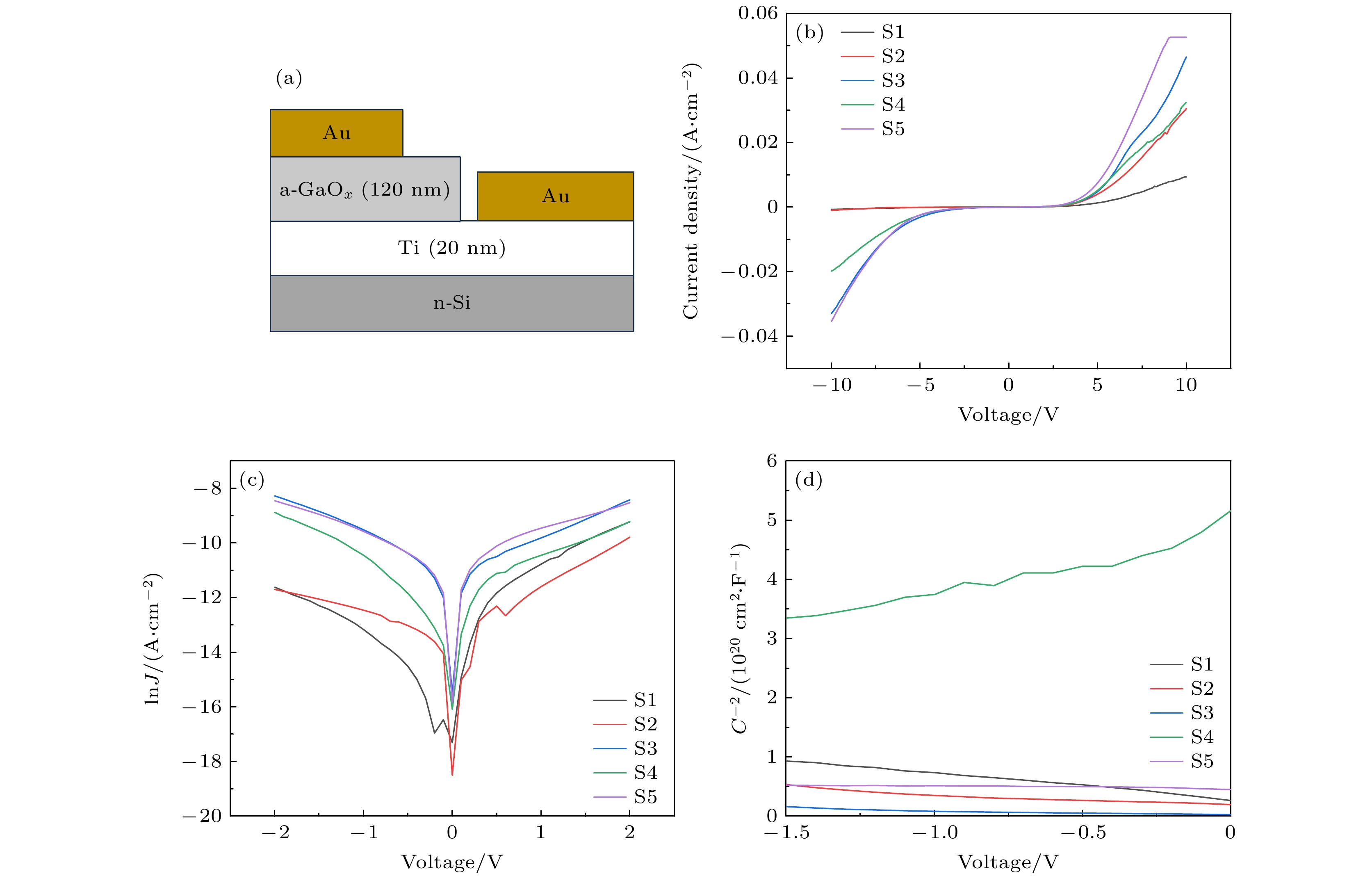
图 5 a-GaOx Schottky器件 (a)结构图; (b) J-V特性曲线; (c) lnJ-V特性曲线; (d) 1/C2-V特性曲线
Fig. 5. a-GaOx Schottky device: (a) Structure; (b) J-V curves; (c) lnJ-V curves; (d) 1/C2-V curves.
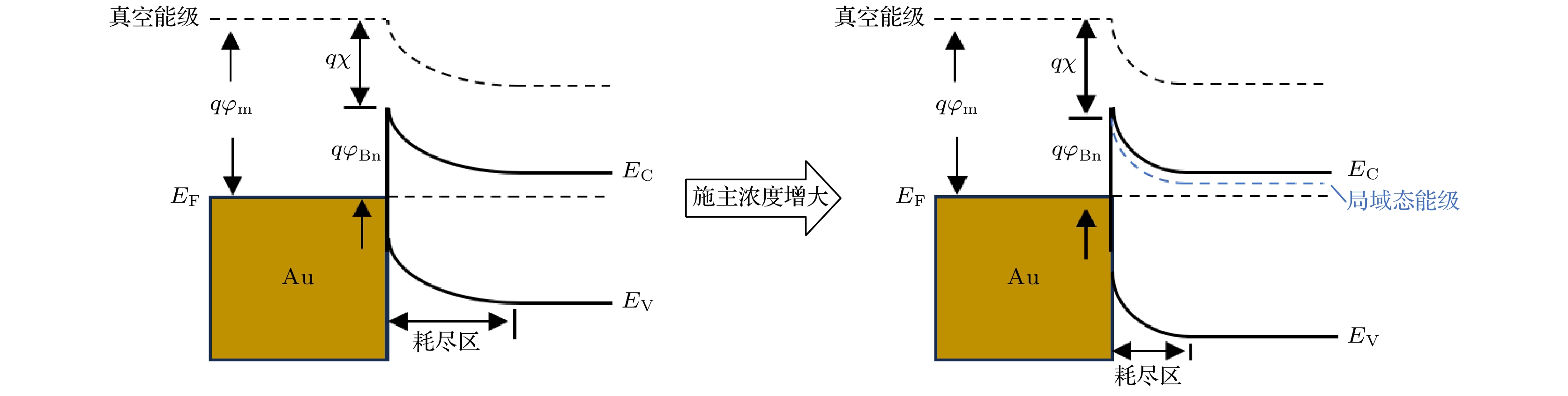
图 6 Au/a-GaOx界面处能带结构示意图
Fig. 6. Schematic diagram of the band structure at the Au/a-GaOx interface.
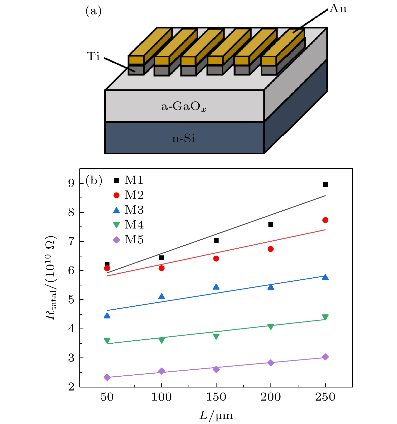
图 7 (a) TLM结构示意图; (b) a-GaOx的 Rtatal -L关系图
Fig. 7. (a) Schematic diagram of TLM structure; (b) diagrams Rtatal -L of a-GaOx.
表 1 a-GaOx中各元素原子百分比与O/Ga比
Table 1. Percentage of atoms of each element and O/Ga ratio in a-GaOx.
样品 O/% Ga/% Si/% O/Ga比 氧气流量/(cm3·min–1) N1 79.31 20.37 0.32 3.89 0 N2 77.33 21.19 1.48 3.64 2 N3 77.11 21.57 1.32 3.57 3 N4 77.37 21.73 0.91 3.56 4 N5 76.60 22.57 0.83 3.39 5  下载: 导出CSV
表 2 a-GaOx的Eg与EU
Table 2. Eg and EU of a-GaOx.
样品 N1 N2 N3 N4 N5 Eg /eV 5.200 5.237 5.271 5.277 5.282 EU/eV 0.337 0.349 0.408 0.411 0.422 O/Ga比 3.89 3.64 3.57 3.56 3.39 氧气流量/(cm3·min–1) 0 2 3 4 5
下载: 导出CSV
表 3 a-GaOx的氧空位浓度与Ga1+浓度
Table 3. Oxygen Vacancy Concentration and Ga1+ Concentration in a-GaOx.
样品 S1 S2 S3 S4 S5 O/Ga比 3.89 3.64 3.57 3.56 3.39 氧空位浓度/% 36 35 38 40 38 Ga1+浓度/% 58 62 67 68 76
下载: 导出CSV
表 4 Au/a-GaOx界面的理想因子n与势垒$ {\varphi _{{\text{Bn}}}} $
Table 4. Ideal factors n and potential barriers $ {\varphi _{{\text{Bn}}}} $ of Au/ a-GaOx interface.
样品 S1 S2 S3 S4 S5 n 1.663 1.397 1.041 1.395 0.923 $ {\varphi _{{\text{Bn}}}} $/V 0.867 0.866 0.812 0.803 0.797 $ q\chi $/eV 4.233 4.234 4.288 4.297 4.303 $ {R_{{\text{on, sp}}}} $ /(Ω·cm2) 1483 413 332 305 208
下载: 导出CSV
表 5 a-GaOx的TLM结构的接触电阻率rc与片电阻Rsheet
Table 5. Contact resistivity rc and chip resistance Rsheet of the TLM structure of a-GaOx.
样品 M1 M2 M3 M4 M5 rc/(Ω·mm) 2.63×10⁹ 2.71×10⁹ 2.17×10⁹ 2.08×10⁹ 1.70×10⁹ Rsheet/
(Ω·□–1)1.33×10¹⁰ 7.94×10⁹ 5.94×10⁹ 4.16×10⁹ 3.39×10⁹
下载: 导出CSV
-
[1] Wang Y F, Su J, Lin Z H, Zhang J C, Chang J J, Hao Y 2022 J. Mater. Chem. C 10 13395
 Google Scholar
[2] Wang Y F, Xue Y X, Su J, Lin Z H, Zhang J C, Chang J J, Hao Y 2022 Mater. Today Adv. 16 100324
Google Scholar
[3] Peelaers H, Van de Walle C G 2015 Phys. Status Solidi (a) 252 828
Google Scholar
[4] Segura A, Artús L, Cuscó R, Goldhahn R, Feneberg M 2017 Phys. Rev. Mater. 1 024604
Google Scholar
[5] Vu T K O, Lee D U, Kim E K 2019 J. Alloys Compd. 806 874
Google Scholar
[6] Feng X J, Li Z, Mi W, Luo Y, Ma J 2015 Mater. Sci. Semicond. Process. 34 52
Google Scholar
[7] He W, Wang Z X, Zheng T, Wang L Y, Zheng S W 2021 J. Electron. Mater. 50 3856
Google Scholar
[8] Zhang Y J, Yan J L, Li Q S, Qu C, Zhang L Y, Xie W F 2011 Mater. Sci. Eng. B 176 846
Google Scholar
[9] Tak B, Dewan S, Goyal A, Pathak R, Gupta V, Kapoor A, Nagarajan S, Singh R 2019 Appl. Surf. Sci. 465 973
Google Scholar
[10] Kim B G 2021 J. Korean Phys. Soc. 79 946
Google Scholar
[11] Cui S J, Mei Z X, Zhang Y H, Liang H L, Du X L 2017 Adv. Opt. Mater. 5 1700454
Google Scholar
[12] Zhang F, Li H, Cui Y T, Li G L, Guo Q 2018 AIP Adv. 8 045112
Google Scholar
[13] Zhu W H, Xiong L L, Si J W, Hu Z L, Gao X, Long L Y, Li T, Wan R Q, Zhang L, Wang L C 2020 Semicond. Sci. Technol. 35 055037
Google Scholar
[14] An Y H, Guo D Y, Li S Y, Wu Z P, Huang Y Q, Li P G, Li L, Tang W H 2016 J. Phys. D: Appl. Phys. 49 285111
Google Scholar
[15] Zhang Y F, Chen X H, Xu Y, Ren F F, Gu S L, Zhang R, Zheng Y D, Ye J D 2019 Chin. Phys. B 28 028501
Google Scholar
[16] Akiyama T, Kawamura T, Ito T 2023 Appl. Phys. Express 16 015508
Google Scholar
[17] Li W X, Wan J X, Tu Z X, Li H, Wu H, Liu C 2022 Ceram. Int. 48 3185
Google Scholar
[18] Heinemann M D, Berry J, Teeter G, Unold T, Ginley D 2016 Appl. Phys. Lett. 108 022107
Google Scholar
[19] Zhang J L, Yuan Y D, Yang X T, Zheng Y J, Zhang H G, Zeng G G 2023 J. Phys. D: Appl. Phys. 56 085103
Google Scholar
[20] Ding J Q, Liu Y, Gu X Y, Zhang L, Zhang X D, Chen X, Liu W J, Cai Y, Guo S S, Sun C L 2024 Physica B 682 415888
Google Scholar
[21] Lyle L A, Back T C, Bowers C T, Green A J, Chabak K D, Dorsey D L, Heller E R, Porter L M 2021 APL Mater. 9 061104
Google Scholar
[22] Gopalan P, Knight S, Chanana A, Stokey M, Ranga P, Scarpulla M A, Krishnamoorthy S, Darakchieva V, Galazka Z, Irmscher K 2020 Appl. Phys. Lett. 117 252103
Google Scholar

 下载:
下载:


计量
- 文章访问数: 324
- PDF下载量: 5
- 被引次数: 0
