


-
栅氧化层的经时击穿作为影响互补型金属-氧化物-半导体集成电路可靠性的一个重要因素, 一直是国内外学者研究的重点. 为了对其进一步研究, 首先从栅氧化层在电应力下经时击穿的微观机理出发, 基于栅氧化层中电子陷阱密度累积达到临界值时发生击穿的原理和电子陷阱生成过程的随机性, 提出了栅氧化层经时击穿的非平衡统计理论分析方法, 然后分别给出了恒定电流应力和恒定电压应力下电子陷阱生成速率方程, 导出了电子陷阱密度的概率密度分布函数. 最后以具体器件为例进行分析, 得到了栅氧化层的最概然寿命随电流应力、电压应力及其厚度的变化规律, 并类比固体断裂现象中“疲劳极限”的概念定义“击穿极限”概念. 计算出了累积失效率随电流应力、电压应力和时间的变化规律, 引入特征值来描述累积失效率达到0.63所用的时间. 结果表明: 电子陷阱密度的概率密度分布函数满足对数正态分布, 且理论结果与实验结果相符.As one of the important factors affecting the reliability of Complementary metal oxide semiconductor integrated circuits, the time-dependent dielectric breakdown of gate oxide has always been the focus of domestic and foreign scientists. The previous researches have shown that when the electrons pass through the silicon dioxide lattice and collide with it, part of their kinetic energy will be dissipated, then among of which can create some sort of defects that behave as electron traps. However, when the electron traps density reaches a critical value in the gate oxide, the destructive thermal effects open a low-resistance ohmic path between the electrodes, thus, triggering the breakdown conducting mechanism. In this paper, in order to employing a statistical theoretical analysis method, the behavior related with time-dependent dielectric breakdown of gate oxide was investigated in detail. The following useful results are obtained, (i) According to the microscopic mechanism of the time-dependent dielectric breakdown of gate oxide under electrical stresses associated with the randomness and irreversibility of the electron traps generation in gate oxide, a theoretical analysis method has been proposed, which is based on the equation of the electron traps generation rate combined with the Langevin equation in random theory and the Fokker-Planck equation in the non-equilibrium statistical theory. (ii) In light of the dynamic equilibrium model, the generation rate equations of electron traps under constant current stress and constant voltage stress as well as the probability density distribution functions of electron traps density were determined. By integrating these distribution function, the cumulative failure rate was further obtained. (iii) Taking the specific metal oxide semiconductor capacitors as examples, the relationship between the most probable lifetime of the gate oxide and the constant current stress, constant voltage stress, as well as its thickness have been revealed. And the concept of "breakdown limit" was defined by analogy with the concept of "fatigue limit" in the phenomenon of solid fracture. (iv) The dependence of the cumulative failure rate on the current stress, voltage stress, and time has been presented. A characteristic value of the time was introduced to indicate the time when the cumulative failure rate reaches 0.63. At this time, most devices have breakdown failure. Besides, the test parameters are not affected by previous failures, and they are close to that of the cumulative failure rate of 1. The results show that the probability density distribution function of electron traps density satisfies lognormal distribution, and the obtained distribution of failures fits well with the experimental statistical data.
-
Keywords:
- gate oxide /
- time-dependent dielectric breakdown /
- nonequilibrium statistical theory /
- cumulative failure
[1] 简维廷, 赵永, 张荣哲 2010 半导体技术 35 154
 Google Scholar
Jane W T, Zhao Y, Zhang R Z 2010 Semicond. Technol. 35 154
Google Scholar
[2] Stathis J H, Linder B P, Rodriguez R, Lombardo S 2003 Microelectron. Reliab. 43 1353
Google Scholar
[3] 王彦刚, 许铭真, 谭长华, 段小蓉 2005 54 3884
Google Scholar
Wang Y G, Xu M Z, Tan C H, Duan C H 2005 Acta Phys. Sin. 54 3884
Google Scholar
[4] 胡恒升, 张敏, 林立谨 2000 电子学报 28 80
Google Scholar
Hu H S, Zhang M, Lin L J 2000 Acta Electron. Sin. 28 80
Google Scholar
[5] Harari E 1978 J. Appl. Phys. 49 2478
Google Scholar
[6] Chen I C, Holland S E, Hu C M 1985 IEEE Trans. Electron Devices 32 413
Google Scholar
[7] Ricco B, Azbel M Y, Brodsky M H 1983 Phys. Rev. Lett. 51 1795
Google Scholar
[8] Apte P P, Saraswat K C 1994 IEEE Trans. Electron Devices 41 1595
Google Scholar
[9] 马仲发, 庄奕琪, 杜磊, 包军林, 李伟华 2003 52 2046
Google Scholar
Ma Z F, Zhuang Y Q, Du L, Bao J L, Li W H 2003 Acta Phys. Sin. 52 2046
Google Scholar
[10] Lee J C, Chen I C, Hu C M 1988 IEEE Trans. Electron Devices 35 2268
Google Scholar
[11] Suñé J, Placencia I, Barnio N, Farrés E, Martin F, Aymerich X 1990 Thin Solid Films 185 347
Google Scholar
[12] Nissan-Cohen Y, Shappir J, Frohman-Bentchkowsky D 1985 J. Appl. Phys. 58 2252
Google Scholar
[13] 姚峰英, 胡恒升, 张敏 2001 电子学报 29 1522
Google Scholar
Yao F Y, Hu H S, Zhang M 2001 Acta Electron. Sin. 29 1522
Google Scholar
[14] Suñé J, Placencia I, Barniol N, Farrés E, Aymerich X 1989 Phys. Status Solidi A 111 675
Google Scholar
[15] 林立谨, 张敏 2000 电子学报 28 59
Google Scholar
Lin L J, Zhang M 2000 Acta Elect. Sin. 28 59
Google Scholar
[16] Dumin D J, Maddux J R, Scott R S, Subramoniam R 1994 IEEE Trans. Electron Devices 41 1570
Google Scholar
[17] [18] 邢修三 1991 材料科学进展 5 22
Google Scholar
Xing X S 1991 Mater. Sci. Prog 5 22
Google Scholar
[19] 杨晓丽, 王斌容, 胡海云 2018 67 180501
Google Scholar
Yang X L, Wang B R, Hu H Y 2018 Acta Phys. Sin. 67 180501
Google Scholar
[20] Kottalam J, Lindenberg K, West B J 1986 J. Stat. Phys. 42 979
Google Scholar
[21] Olivo P, Ricco B, Nguyen T N, Kuan T S, Jeng S J 1987 Appl. Phys. Lett. 51 2245
Google Scholar
[22] Chen C F, Wu C Y, Lee M K, Chen C N 1987 IEEE Trans. Electron Devices 34 1540
Google Scholar
[23] 刘红侠, 郝跃 2002 半导体学报 23 952
Liu H X, Hao Y 2002 Chin. J. Semicond. 23 952
[24] Piyas S 2017 J. Semicond. 38 50
Google Scholar
-
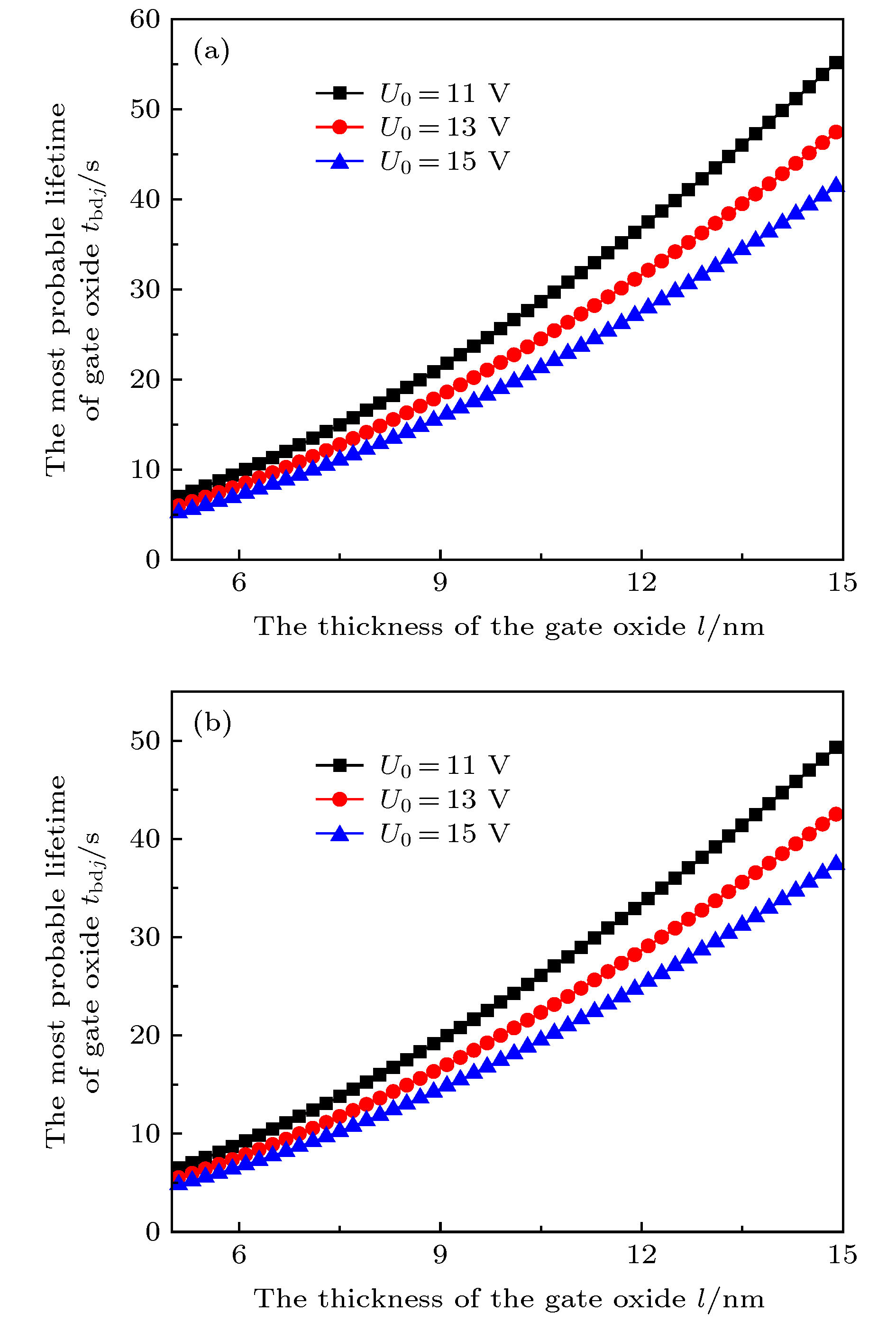
图 1 不同厚度栅氧化层的最概然寿命 (a) 样品1[21],
$J = 1 \;{\rm{A}}/{\rm{c}}{{\rm{m}}^{2}}$ ; (b) 样品2[22],$J = 0.8 \;{\rm{A}}/{\rm{c}}{{\rm{m}}^{2}}$ Fig. 1. The most probable lifetime of gate oxide with different thickness: (a) Sample 1[21] at
$J = 1 \;{\rm{A}}/{\rm{c}}{{\rm{m}}^{2}}$ ; (b) sample 2[22] at$J = 0.8 \;{\rm{A}}/{\rm{c}}{{\rm{m}}^{2}}$ 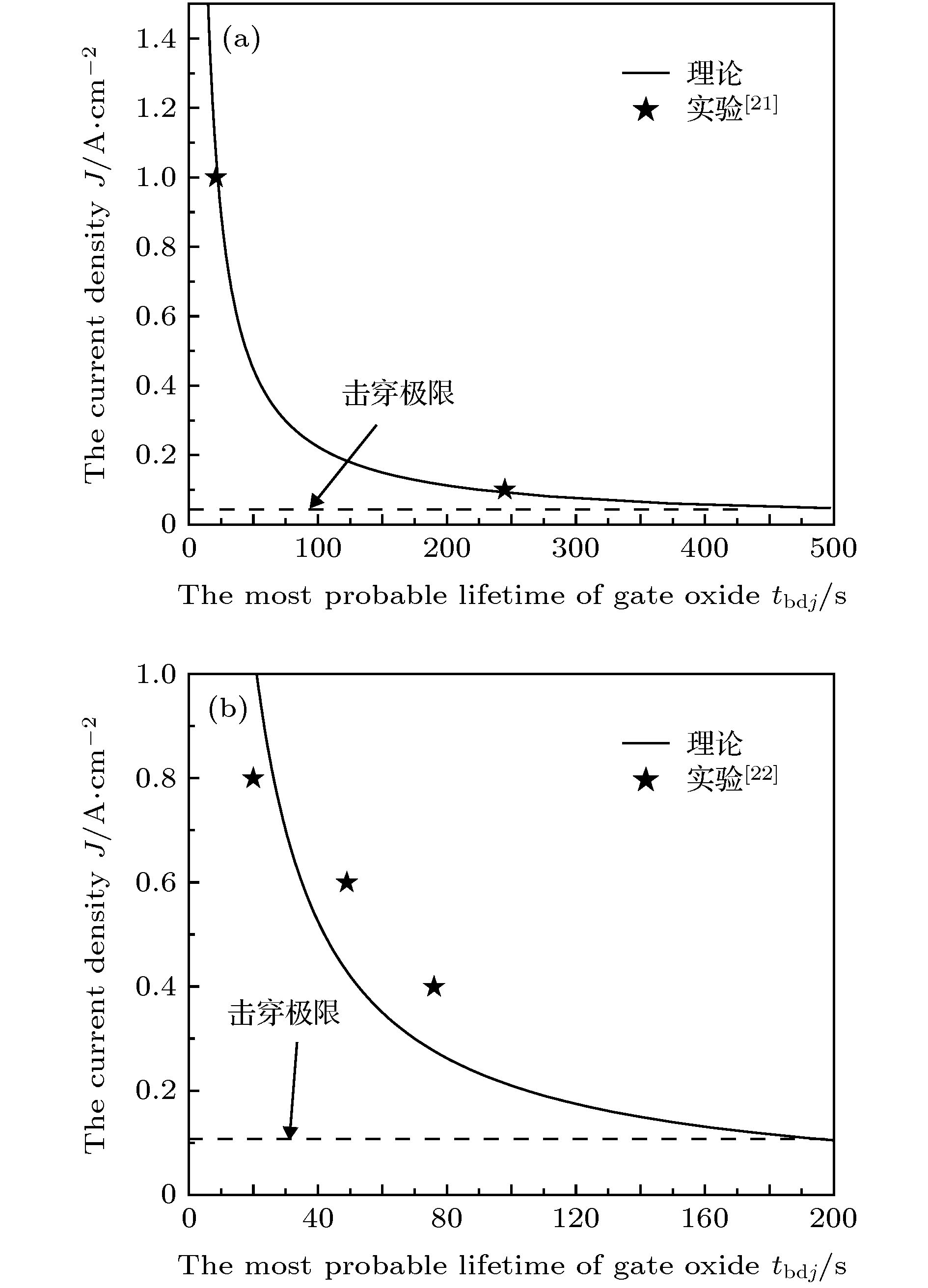
图 2 不同电流密度对应的栅氧化层的最概然寿命 (a) 样品1; (b) 样品2
Fig. 2. The most probable lifetime of gate oxide under different electric current density: (a) Sample 1; (b) sample 2
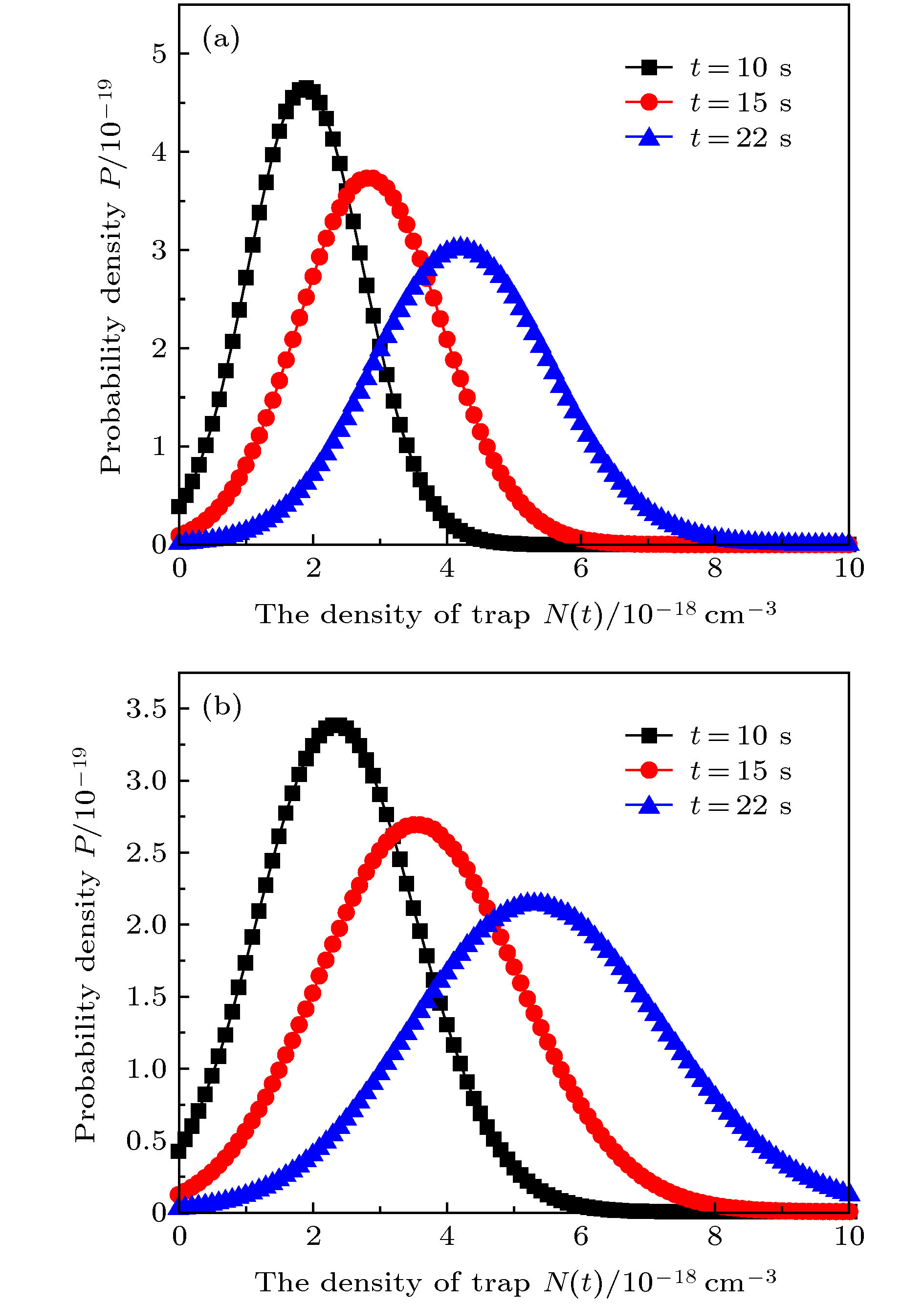
图 3 不同时刻的P-N图 (a) 样品1,
$J = 1\; {\rm{A}}/{\rm{c}}{{\rm{m}}^{2}}$ ; (b) 样品2,$J = 0.8\; {\rm{A}}/{\rm{c}}{{\rm{m}}^{2}}$ Fig. 3. The probability density varies with electron trap density at different time: (a) Sample 1 at
$J = 1\; {\rm{A}}/{\rm{c}}{{\rm{m}}^{2}}$ ; (b) sample 2 at$J = 0.8\; {\rm{A}}/{\rm{c}}{{\rm{m}}^{2}}$ 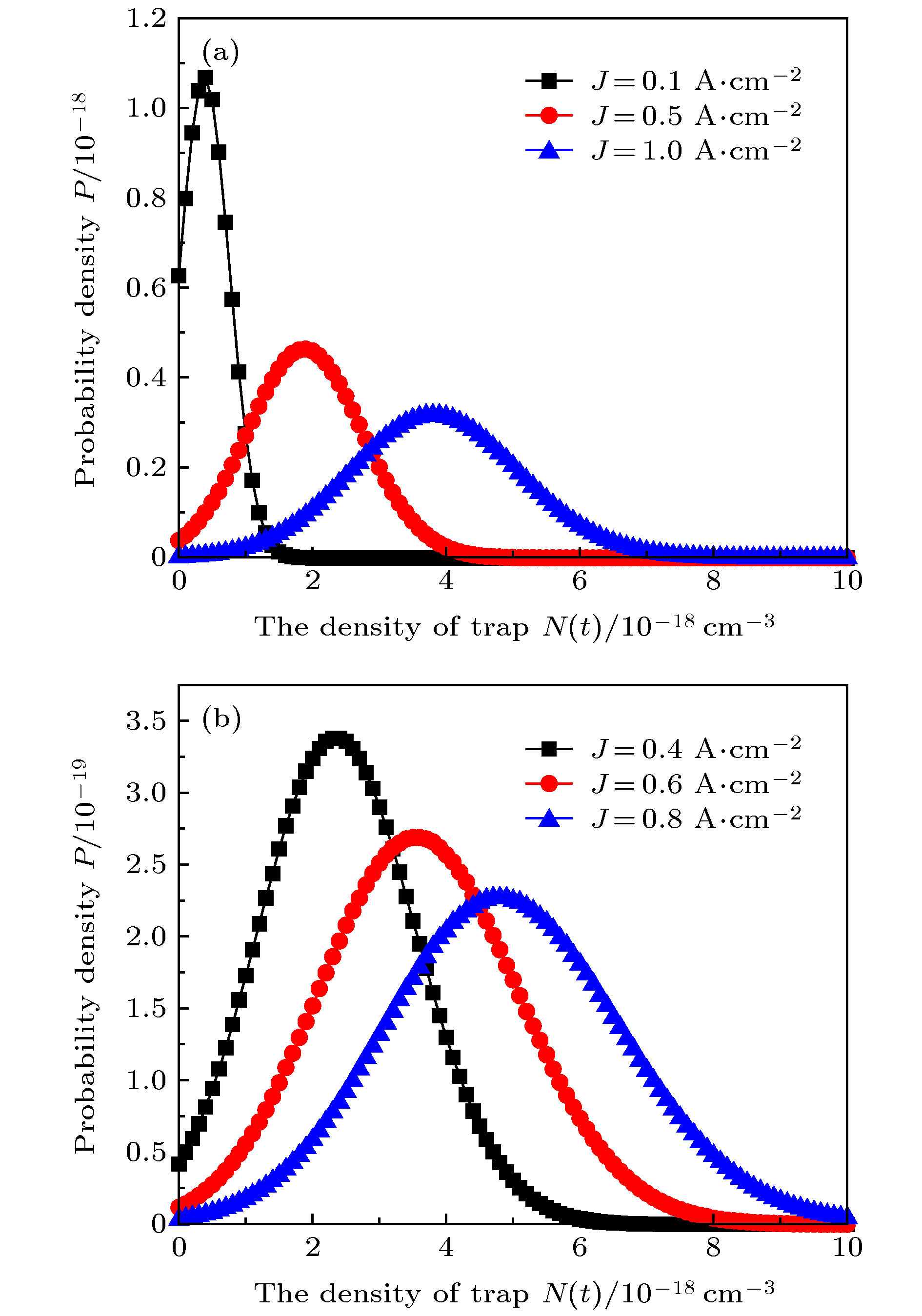
图 4 不同电流密度下的P-N图(
$t = {\rm{2}}0\;{\rm{ s}}$ ) (a) 样品1; (b) 样品2Fig. 4. The probability density varies with electron trap density under different electric current density(
$t = {\rm{2}}0\;{\rm{ s}}$ ): (a) Sample 1; (b) sample 2.
图 5 样品1中两种不同电流密度的累积失效率 (a) J = 0.1 A/ cm2; (b)
$J = 1\;{\rm{A}}/{\rm{c}}{{\rm{m}}^{2}}$ Fig. 5. Breakdown cumulative distributions for two different electric current densities in sample 1: (a) J =
$ 0.1~\rm A/cm^{2} $ ; (b)$J = 1 \;{\rm{A}}/{\rm{c}}{{\rm{m}}^{ 2}}$ 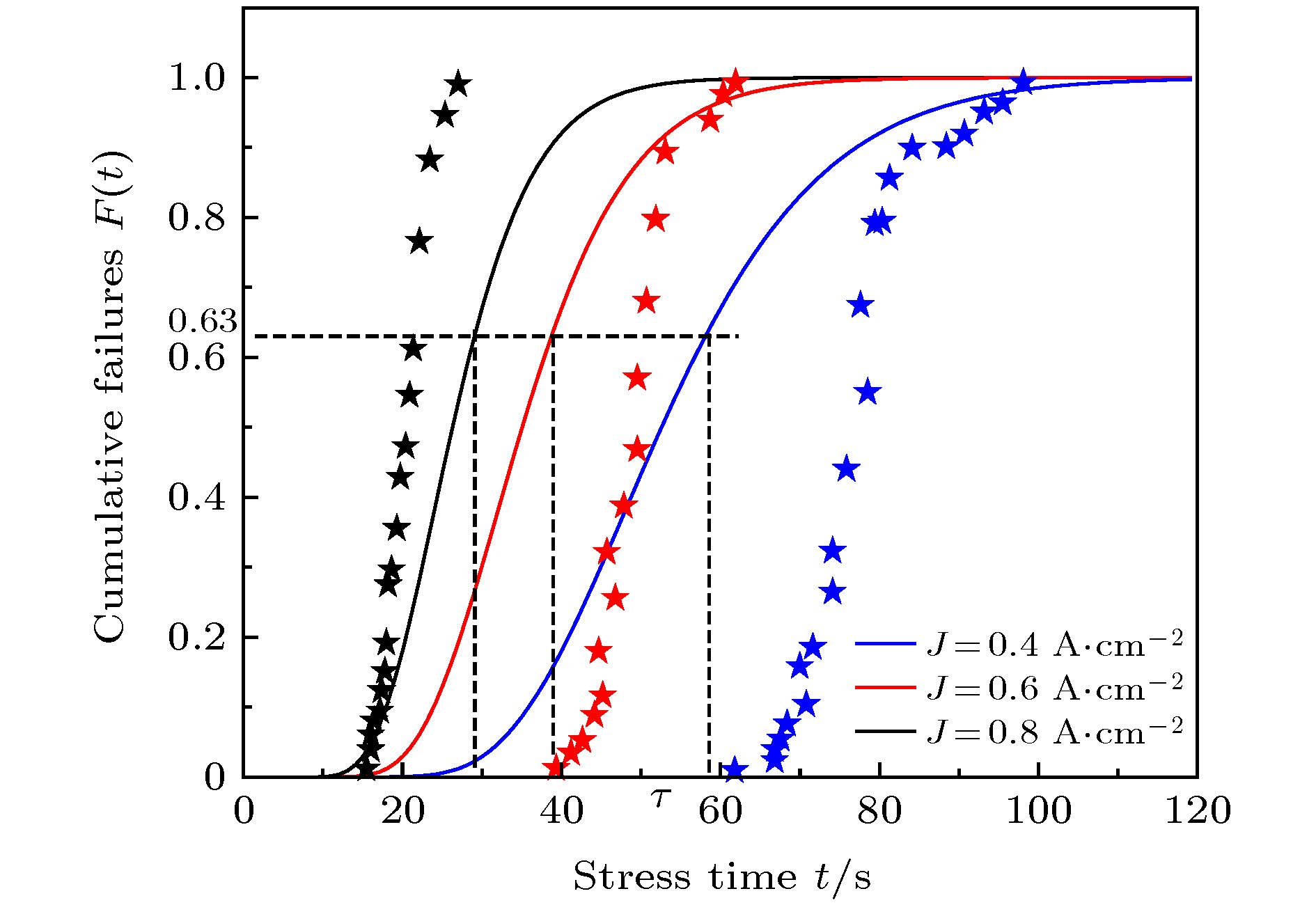
图 6 样品2中三种不同电流密度的累积失效率 (注: 实心五角星代表实验值, 线段代表理论值.)
Fig. 6. Breakdown cumulative distributions for three electric current densities in sample 2. (Note: solid five-pointed star represents experimental value and line segment represents theoretical value.)
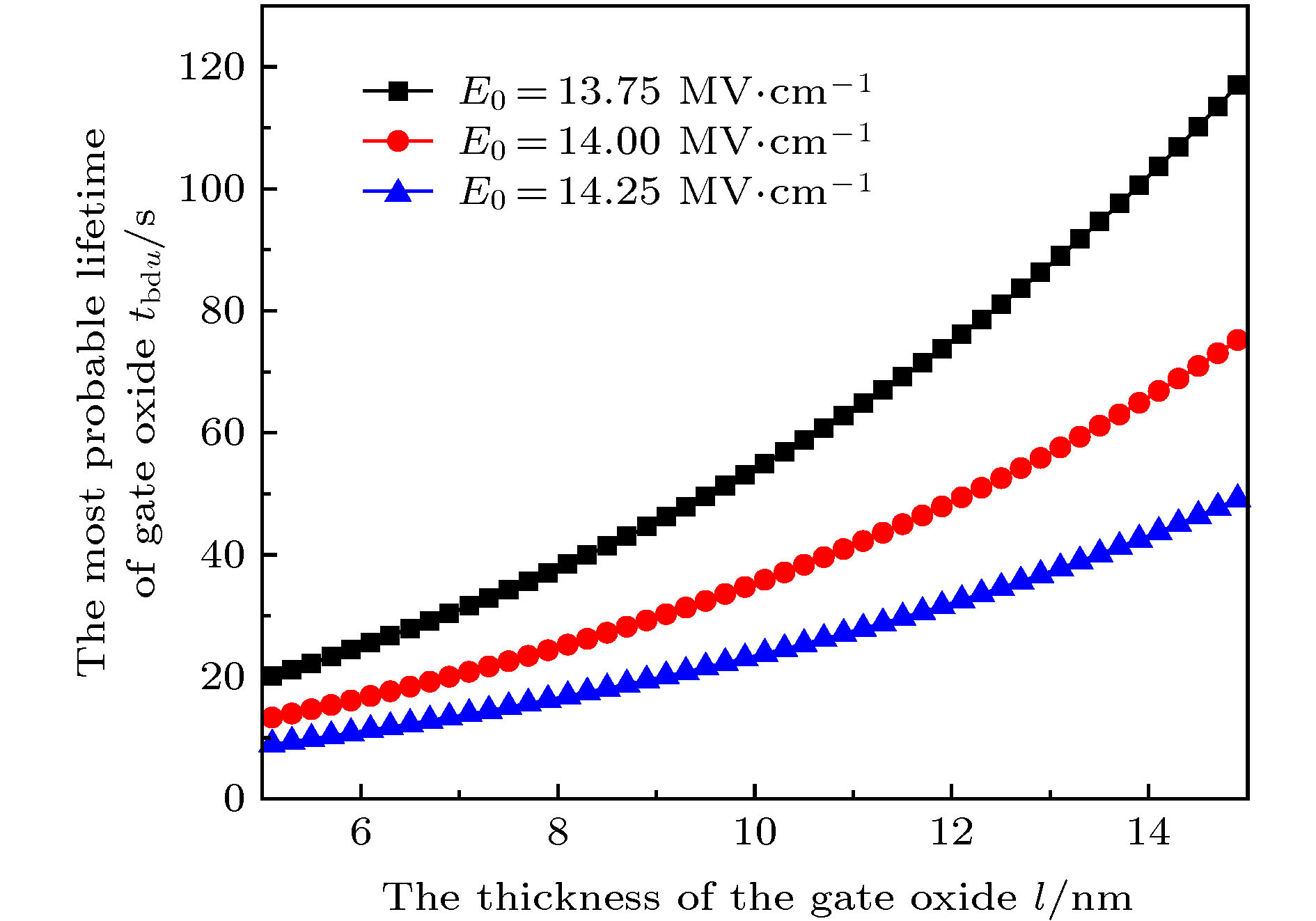
图 7 不同厚度的栅氧化层的最概然寿命
Fig. 7. The most probable lifetime of gate oxide with different thickness.
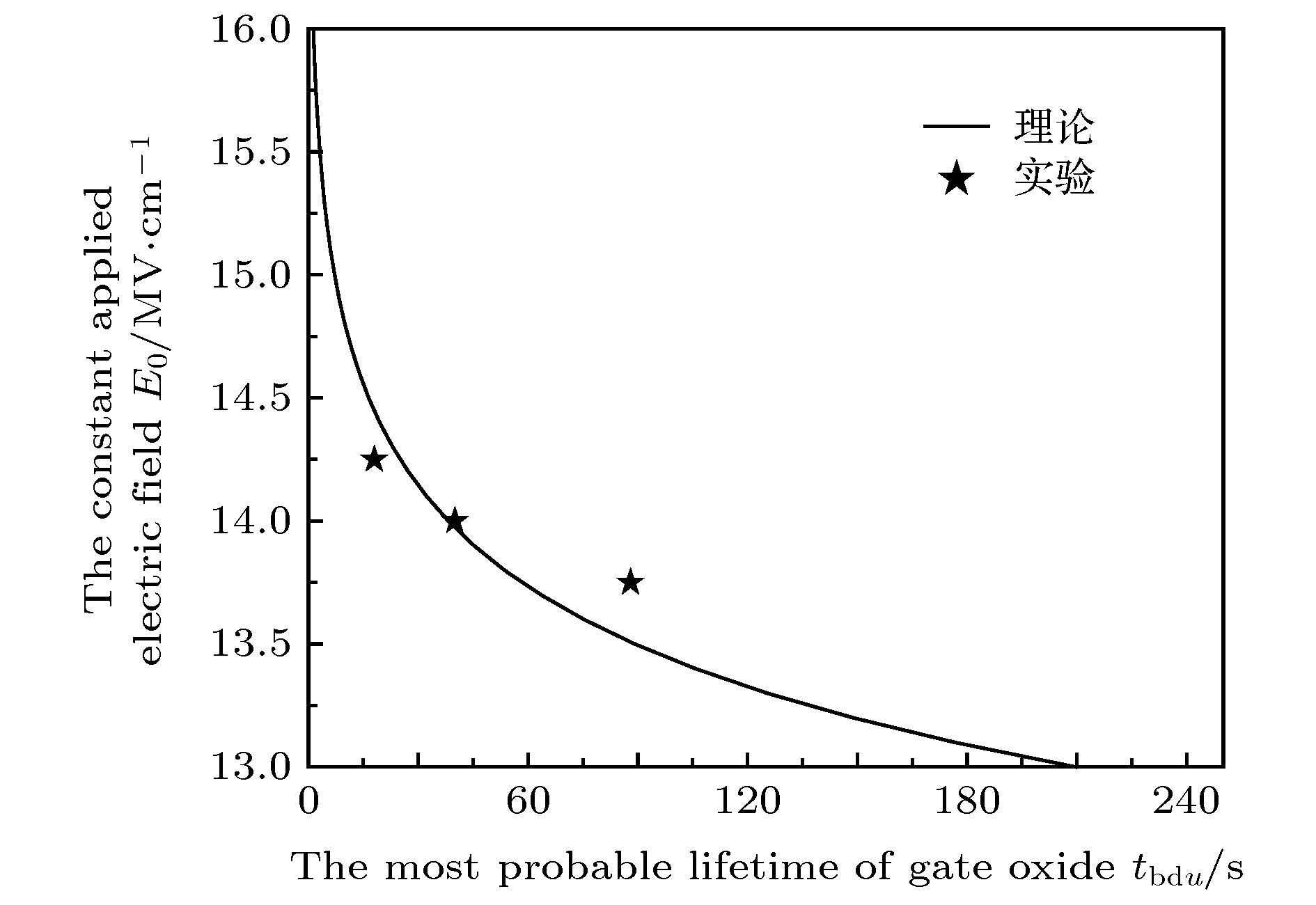
图 8 不同电场强度对应的栅氧化层的最概然寿命
Fig. 8. The most probable lifetime of gate oxide under different electric field.

图 9
${E_0} = 13.75 \;{\rm{MV}} \cdot {\rm{c}}{{\rm{m}}^{ - 1}}$ 时, 不同时刻的P-N图Fig. 9. The probability density varies with electron trap density at different time under
${E_0} = 13.75\; {\rm{MV}} \cdot {\rm{c}}{{\rm{m}}^{ - 1}}$ .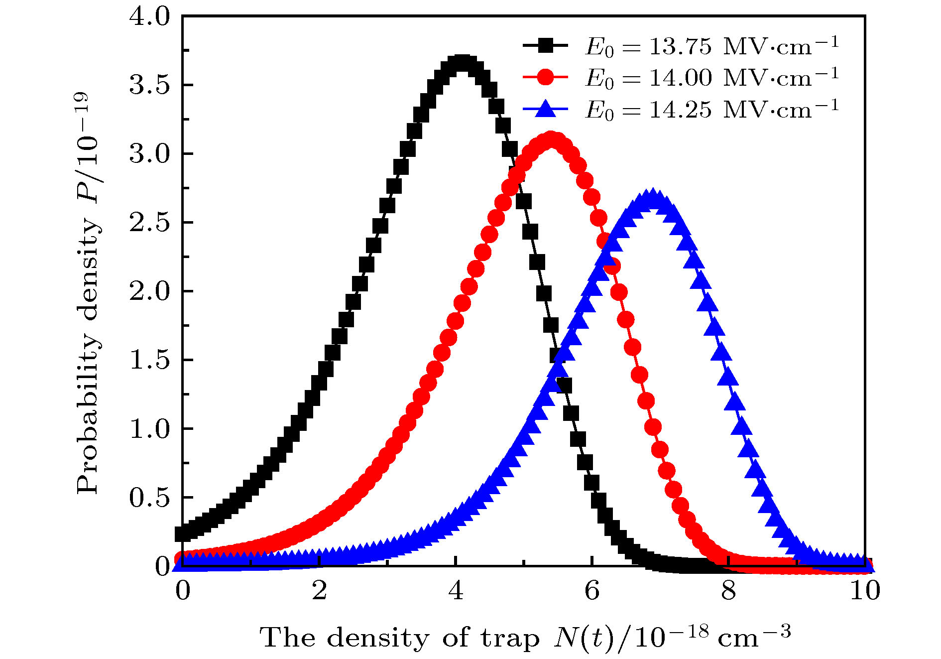
图 10
$t = 30 \;{\rm{s}}$ 时, 不同电场强度下的P-N图Fig. 10. The probability density varies with electron trap density at
$t = {\rm{30\; s}}$ under the different electric field.
图 11 三种不同电压下的累积失效率
Fig. 11. Breakdown cumulative distributions for three different electric field.
-
[1] 简维廷, 赵永, 张荣哲 2010 半导体技术 35 154
Google Scholar
Jane W T, Zhao Y, Zhang R Z 2010 Semicond. Technol. 35 154
Google Scholar
[2] Stathis J H, Linder B P, Rodriguez R, Lombardo S 2003 Microelectron. Reliab. 43 1353
Google Scholar
[3] 王彦刚, 许铭真, 谭长华, 段小蓉 2005 54 3884
Google Scholar
Wang Y G, Xu M Z, Tan C H, Duan C H 2005 Acta Phys. Sin. 54 3884
Google Scholar
[4] 胡恒升, 张敏, 林立谨 2000 电子学报 28 80
Google Scholar
Hu H S, Zhang M, Lin L J 2000 Acta Electron. Sin. 28 80
Google Scholar
[5] Harari E 1978 J. Appl. Phys. 49 2478
Google Scholar
[6] Chen I C, Holland S E, Hu C M 1985 IEEE Trans. Electron Devices 32 413
Google Scholar
[7] Ricco B, Azbel M Y, Brodsky M H 1983 Phys. Rev. Lett. 51 1795
Google Scholar
[8] Apte P P, Saraswat K C 1994 IEEE Trans. Electron Devices 41 1595
Google Scholar
[9] 马仲发, 庄奕琪, 杜磊, 包军林, 李伟华 2003 52 2046
Google Scholar
Ma Z F, Zhuang Y Q, Du L, Bao J L, Li W H 2003 Acta Phys. Sin. 52 2046
Google Scholar
[10] Lee J C, Chen I C, Hu C M 1988 IEEE Trans. Electron Devices 35 2268
Google Scholar
[11] Suñé J, Placencia I, Barnio N, Farrés E, Martin F, Aymerich X 1990 Thin Solid Films 185 347
Google Scholar
[12] Nissan-Cohen Y, Shappir J, Frohman-Bentchkowsky D 1985 J. Appl. Phys. 58 2252
Google Scholar
[13] 姚峰英, 胡恒升, 张敏 2001 电子学报 29 1522
Google Scholar
Yao F Y, Hu H S, Zhang M 2001 Acta Electron. Sin. 29 1522
Google Scholar
[14] Suñé J, Placencia I, Barniol N, Farrés E, Aymerich X 1989 Phys. Status Solidi A 111 675
Google Scholar
[15] 林立谨, 张敏 2000 电子学报 28 59
Google Scholar
Lin L J, Zhang M 2000 Acta Elect. Sin. 28 59
Google Scholar
[16] Dumin D J, Maddux J R, Scott R S, Subramoniam R 1994 IEEE Trans. Electron Devices 41 1570
Google Scholar
[17] [18] 邢修三 1991 材料科学进展 5 22
Google Scholar
Xing X S 1991 Mater. Sci. Prog 5 22
Google Scholar
[19] 杨晓丽, 王斌容, 胡海云 2018 67 180501
Google Scholar
Yang X L, Wang B R, Hu H Y 2018 Acta Phys. Sin. 67 180501
Google Scholar
[20] Kottalam J, Lindenberg K, West B J 1986 J. Stat. Phys. 42 979
Google Scholar
[21] Olivo P, Ricco B, Nguyen T N, Kuan T S, Jeng S J 1987 Appl. Phys. Lett. 51 2245
Google Scholar
[22] Chen C F, Wu C Y, Lee M K, Chen C N 1987 IEEE Trans. Electron Devices 34 1540
Google Scholar
[23] 刘红侠, 郝跃 2002 半导体学报 23 952
Liu H X, Hao Y 2002 Chin. J. Semicond. 23 952
[24] Piyas S 2017 J. Semicond. 38 50
Google Scholar


 下载:
下载:


计量
- 文章访问数: 8371
- PDF下载量: 79
- 被引次数: 0
